
¸
4-43
4
GEN
E
RA
L
P
URPO
S
E
A
M
P
L
IF
IE
RS
Product Description
Ordering Information
Typical Applications
Features
Functional Block Diagram
RF Micro Devices, Inc.
7625 Thorndike Road
Greensboro, NC 27409, USA
Tel (336) 664 1233
Fax (336) 664 0454
http://www.rfmd.com
Optimum Technology MatchingÆ Applied
Si BJT
GaAs MESFET
GaAs HBT
Si Bi-CMOS
SiGe HBT
Si CMOS
1
2
3
6
5
4
VCC
GND
RF IN
RF OUT
GND
GC
ATT
ATT
RF2377
PCS/CELLULAR TDMA/CDMA/W-CDMA
LINEAR VARIABLE GAIN AMPLIFIER
∑ CDMA PCS/Cellular Handsets
∑ TDMA PCS/Cellular Handsets
∑ W-CDMA Handsets
The RF2377 is a linear variable gain amplifier suitable for
use in TDMA and CDMA systems in the cellular or PCS
band and for W-CDMA systems. The features of this
device include linear gain control, high gain, and high lin-
earity. The IC is manufactured on an advanced Gallium
Arsenide Heterojunction Bipolar Transistor (GaAs HBT)
process and is featured in an industry-standard miniature
6-lead plastic SOT package.
∑ 50dB Linear Gain Control Range
∑ 24dB Maximum Gain
∑ Single 2.7V to 3.3V Supply
∑ 45mA Supply Current
∑ High Linearity
RF2377
PCS/Cellular TDMA/CDMA/W-CDMA Linear Vari-
able Gain Amplifier
RF2377-410 PCBAFully Assembled Evaluation Board, PCS
RF2377-411 PCBAFully Assembled Evaluation Board, W-CDMA
4
Rev A9 010411
.90
.70
.10 MAX.
1.30
1.00
3.10
2.70
.37 MIN.
3.00
2.60
1.90
.25
.10
.50
.35
1.80
1.40
9∞
T
EXT
*
*When Pin 1 is in
upper left, text
reads downward
(as shown).
All dimensions in mm.
1∞
Package Style: SOT23-6

4-44
RF2377
Rev A9 010411
4
GEN
E
RA
L
P
URPO
S
E
A
M
P
L
IF
IE
RS
Absolute Maximum Ratings
Parameter
Rating
Unit
Supply Voltage
0 to +5.0
V
DC
DC Current
100
mA
Operating Ambient Temperature
-20 to +85
∞C
Storage Temperature
-40 to +150
∞C
Parameter
Specification
Unit
Condition
Min.
Typ.
Max.
Overall
V
CC
= 2.8V, V
GC
= 2.0V, T= 25∞C
Usable Frequency Range
800 to 2200
MHz
Linear Gain Control Range
50
dB
Gain Control Slope
70
dB/V
TDMA
V
CC
= 2.8V, V
GC
= 2.0V, T= 25∞C
Operating Frequency
1880
MHz
Maximum Small Signal Gain
22
24
27
dB
Input VSWR
1.5:1
2.5:1
Over entire gain control range
Output IP3
+23
+26
dBm
Noise Figure
7
dB
Maximum gain
Maximum Average Output Power
+8
dBm
TDMA modulation
Adjacent Channel Power
Rejection
-33
-32
dBc
TDMA modulation; P
OUT
=+8dBm
Alternate Channel Power
Rejection
-61
-57
dBc
TDMA modulation; P
OUT
=+8dBm
CDMA
V
CC
= 2.8V, V
GC
= 2.0V, T= 25∞C
Operating Frequency
1880
MHz
Maximum Small Signal Gain
22
24
27
dB
Input VSWR
1.5:1
2.5:1
Over entire gain control range
Output IP3
+23
+26
dBm
Noise Figure
7
dB
Maximum gain
Maximum Average Output Power
+11
dBm
CDMA modulation; V
CC
= 3.0V, maximum
gain setting, ACPR<-52dBc.
Adjacent Channel Power
Rejection
-53
dBc
CDMA modulation; V
CC
= 3.0V. For
P
IN
> -16dBm, adjustment of P
IN
is required
to maintain ACPR performance over gain
control range. For P
IN
< -16dBm, ACPR per-
formance is maintained over entire gain con-
trol range.
W-CDMA
V
CC
= 2.8V, T= 25∞C
Operating Frequency
1920 to 1980
MHz
Small Signal Gain
20
22
24
dB
V
GC
= 2.0V
-33
-32
-31
dB
V
GC
= 0.3V
Input VSWR
1.5:1
2.5:1
Over entire gain control range
Output IP3
+22
+24
dBm
Noise Figure
4
5
6
dB
Maximum gain
32
32.5
34
dB
Minimum gain
Maximum Linear Output Power
+8
+9
dBm
W-CDMA ACPR<-46dBc, V
GC
=2.0V
Adjacent Channel Power
Rejection
-48
-46
dBc
W-CDMA modulation; V
GC
=2.0V,
P
IN
<-12dBm
-43
dBc
W-CDMA modulation; Over entire gain con-
trol range, P
IN
< -17dBm
-43
dBc
W-CDMA modulation; V
GC
=1.0V,
P
IN
<-14dBm
Caution! ESD sensitive device.
RF Micro Devices believes the furnished information is correct and accurate
at the time of this printing. However, RF Micro Devices reserves the right to
make changes to its products without notice. RF Micro Devices does not
assume responsibility for the use of the described product(s).

4-45
RF2377
Rev A9 010411
4
GEN
E
RA
L
P
URPO
S
E
A
M
P
L
IF
IE
RS
Parameter
Specification
Unit
Condition
Min.
Typ.
Max.
Power Supply
T = 25∞C
Supply Voltage
2.8
V
Specifications
2.7 to 3.3
V
Operating range
Gain Control Voltage
0 to 2.0
V
Supply Current
40
45
60
mA
V
CC
= 2.8V, V
GC
= 2.0V
56
mA
V
CC
= 3.0V, V
GC
= 2.0V
20
mA
V
CC
= 2.8V, V
GC
= 0.4V
V
GC
Current
1.5
mA

4-46
RF2377
Rev A9 010411
4
GEN
E
RA
L
P
URPO
S
E
A
M
P
L
IF
IE
RS
Application Schematic
W-CDMA Application Schematic
Pin
Function
Description
Interface Schematic
1
RF OUT
RF output pin. This pin is DC coupled and requires V
CC
through a bias
inductor sized accordingly to provide a high pass transformation with a
series capacitor.
2
GND
Ground connection. Keep traces physically short and connect immedi-
ately to ground plane for best performance.
3
GC
Analog gain control pin. This pin controls the gain of the IC. Minimum
gain occurs at V
GC
< 0.4V and maximum gain is achieved with
V
GC
= 2.0V. 50dB of linear gain control with little variation of input P
1dB
is available.
4
RF IN
RF input pin. This pin is DC coupled.
5
GND
Ground connection. Keep traces physically short and connect immedi-
ately to ground plane for best performance.
6
VCC
Power supply. This pin should be connected to a regulated supply and
requires a bypass capacitor. Voltage is supplied through this pin to the
first stage collector; this voltage also controls the bias. Gain may be
tuned by adjusting the value of the feed inductor.
RF IN
4
5
6
3
2
1
Note orientation of
package in this schematic.
1 pF
GC
4.7 nH
47 nF
VCC
RF OUT
3.3 nH
47 nH
VCC
ATT
ATT
100 pF
RF IN
4
5
6
3
2
1
Note orientation of
package in this schematic.
1.2 pF
GC
4.7 nH
15 pF
VCC
2.7 nH
47 nH
VCC
ATT
ATT
15 pF
0.5 pF
2.2 nH
29 nH
29 nH
15 pF
1 uF
RF OUT

4-47
RF2377
Rev A9 010411
4
GEN
E
RA
L
P
URPO
S
E
A
M
P
L
IF
IE
RS
Evaluation Board Schematic
(W-CDMA)
Evaluation Board Schematic
(PCS)
Note orientation of
package in this schematic.
C6
1.2 pF
L2
4.7 nH
C3
15 pF
L3
2.7 nH
C4
47 nH
VREG/VCC
J2
RF OUT
C5
15 pF
50
µ
strip
J1
RF IN
VREG/VCC
VGC
C1
15 pF
4
5
6
3
2
1
ATT
ATT
C2
0.5 pF
C7
0.5 pF
L1
2.2 nH
L4
47 nH
L5
47 nH
2377401-
VGC
P1-1
GND
VREG/VCC
P1-3
P1-4
GND
P1
1
2
3
4
5
VREG/VCC
C16
1
µ
F
+
Note orientation of
package in this schematic.
C6
1.2 pF
L2
4.7 nH
C3
47 nF
L3
2.2 nH
C4
47 nH
J2
RF OUT
J1
RF IN
VREG
VGC
C1
100 pF
4
5
6
3
2
1
ATT
ATT
C5
47 nF
C16
1 uF
+
VREG/VCC
2377400A
R1
0 k
P1-4
P1
1
2
3
4
5
VGC
P1-1
GND
VCC
P1-3
GND
4-48
RF2377
Rev A9 010411
4
GEN
E
RA
L
P
URPO
S
E
A
M
P
L
IF
IE
RS
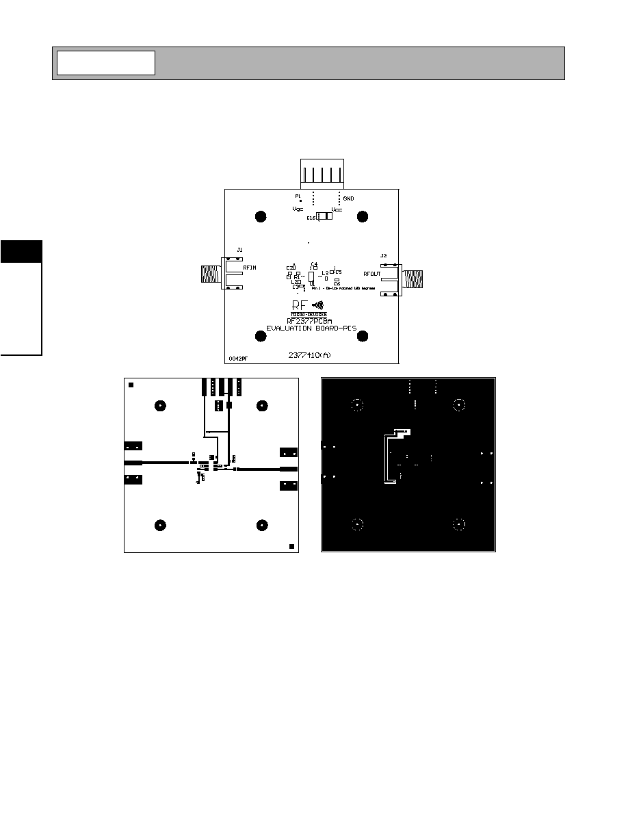
Evaluation Board Layout (PCS)
Board Size 2.0" x 2.0"
Board Thickness 0.028", Board Material FR-4

4-49
RF2377
Rev A9 010411
4
GEN
E
RA
L
P
URPO
S
E
A
M
P
L
IF
IE
RS
Evaluation Board Layout (W-CDMA)
Board Size 2.0" x 2.0"
Board Thickness 0.028", Board Material FR-4

4-50
RF2377
Rev A9 010411
4
GEN
E
RA
L
P
URPO
S
E
A
M
P
L
IF
IE
RS
W-CDMA ACPR versus V
GC
at Various
Maximum Output Powers; V
CC
= 2.8 V, Freq = 1950 MHz
-60.0
-55.0
-50.0
-45.0
-40.0
-35.0
0.8
1.0
1.2
1.4
1.6
1.8
2.0
V
GC
(V)
ACPR
(dBc)
Max Pout=+2dBm
Max Pout=+3dBm
Max Pout=+4dBm
Max Pout=+6dBm
Max Pout=+8dBm
Note: Below V
GC
=~0.9V,
test equipment noise floor inhibits
accurate ACP measurement
Gain versus V
GC
over Temperature
W-CDMA Board; V
CC
= 2.8V, Freq = 1950 MHz
-30.0
-20.0
-10.0
0.0
10.0
20.0
30.0
0.4
0.6
0.8
1.0
1.2
1.4
1.6
1.8
2.0
V
GC
(V)
Gain
(dB)
T = -20∞C
T = +25∞C
T = +85∞C
I
CC
versus V
GC
over Temperature
W-CDMA Board; V
CC
= 2.8V, Freq = 1950 MHz
0.0
10.0
20.0
30.0
40.0
50.0
60.0
0.4
0.6
0.8
1.0
1.2
1.4
1.6
1.8
2.0
V
GC
(V)
I
CC
(mA)
T = -20∞C
T = +25∞C
T = +85∞C
SWR versus V
GC
W-CDMA Board; V
CC
= 2.8 V, Freq = 1950 MHz
0.0
0.5
1.0
1.5
2.0
2.5
3.0
3.5
0.4
0.6
0.8
1.0
1.2
1.4
1.6
1.8
2.0
V
GC
(V)
SWR
Input
Output
Noise Figure versus V
GC
W-CDMA Board; V
CC
= 2.8 V, Freq = 1950 MHz
0.0
5.0
10.0
15.0
20.0
25.0
30.0
35.0
0.4
0.6
0.8
1.0
1.2
1.4
1.6
1.8
2.0
V
GC
(V)
Noise
F
igure
(
dB)