
9-19
9
A
T
T
E
NT
U
A
T
O
RS
AN
D
SWI
T
CH
ES
Product Description
Ordering Information
Typical Applications
Features
Functional Block Diagram
RF Micro Devices, Inc.
7625 Thorndike Road
Greensboro, NC 27409, USA
Tel (336) 664 1233
Fax (336) 664 0454
http://www.rfmd.com
Optimum Technology MatchingÆ Applied
Si BJT
GaAs MESFET
GaAs HBT
Si Bi-CMOS
¸
SiGe HBT
Si CMOS
1
2
3
4
8
7
6
5
IN1
GND
VDD
OUT2
OUT1
GND
CTRL
IN2
RF2425
4-PORT TRANSFER SWITCH
∑ Cordless Phones
∑ Wireless Computer Peripherals
∑ Wireless Security Systems
∑ General Purpose RF Switching
∑ Commercial and Consumer Systems
The RF2425 is a very low-cost single-throw, double-pole
GaAs MESFET switch. There are two bidirectional input/
output channels which can be turned off or on by a single
logic control line. Two of the ports may be tied together
externally to make a transmit/receive switch. The device
can handle power levels as high as +32 dBm and spans a
frequency range from DC to 2000MHz. The switch will
operate from power supply voltages as low as 1.5 V and
as high as 6V with a CMOS logic driver for the control
input.
∑ Single Power Supply of 1.5V to 6.0V
∑ Low Current Consumption
∑ 0.5dB Insertion Loss at 900MHz
∑ 24dB Crosstalk Isolation at 900MHz
∑ +31dBm Output P1dB
RF2425
4-Port Transfer Switch
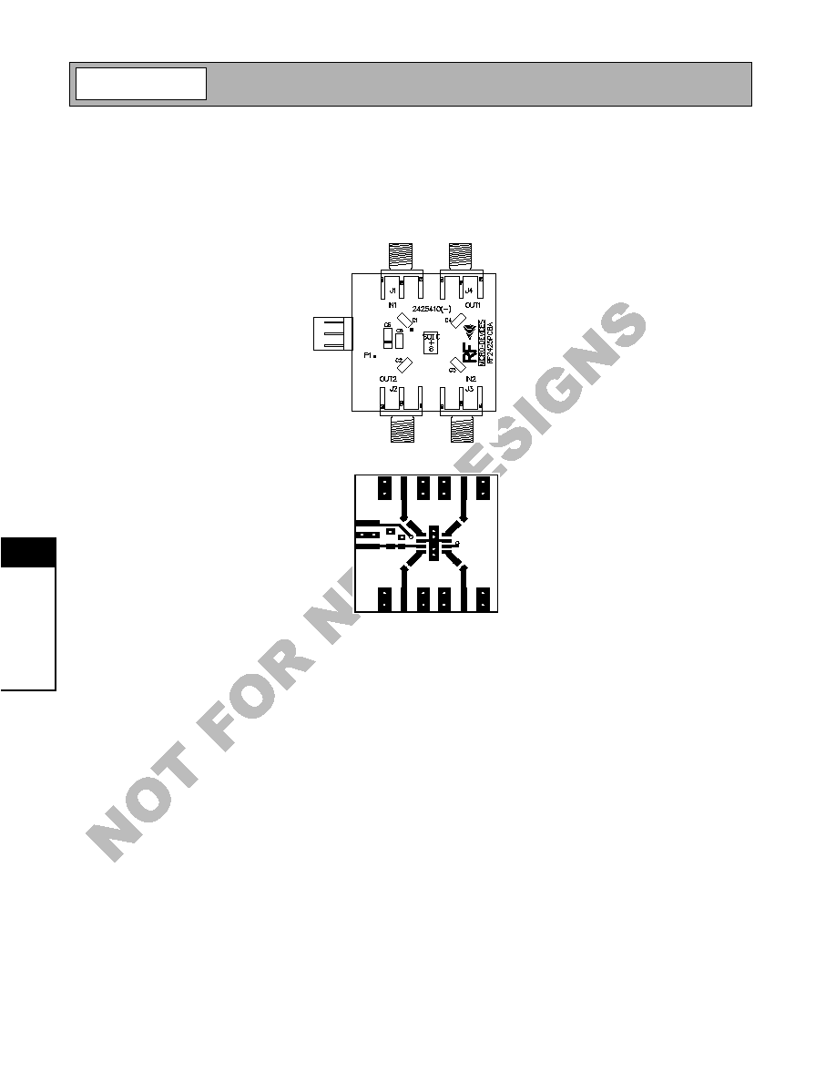
RF2425 PCBA
Fully Assembled Evaluation Board
9
Rev A1 010228
.156
.152
.022
.018
5∞
.056
.052
.195
.191
.240
.232
.050
.008
.004
MIN
.017
1
Package Style: SOP-8

9-20
RF2425
Rev A1 010228
9
A
T
T
E
NT
U
A
T
O
RS
AN
D
SWI
T
CH
ES
Absolute Maximum Ratings
Parameter
Rating
Unit
Supply Voltage
0 to +8.0
V
DC
Control Voltage
-1.0 to +6.0
V
DC
Input RF Power
+33
dBm
Operating Ambient Temperature
-40 to +85
∞C
Storage Temperature
-40 to +150
∞C
Parameter
Specification
Unit
Condition
Min.
Typ.
Max.
Overall
T = 25 ∞C, V
DD
= 3.0V, Freq= 900MHz
Frequency Range
DC to 2000
MHz
Insertion Loss
0.5
1
dB
Isolation
20
24
dB
CTRL= "Low;" IN1 to OUT2 crosstalk
20
24
dB
CTRL= "High;" IN2 to OUT1 crosstalk
"On" Input VSWR
1:1
Input of active channel
"Off" Input VSWR
100:1
Input of inactive channel (open circuit)
Output P1dB
+31
dBm
Control Logic
CTRL Logic "Low" Voltage
0
V
Channel 1 On, Channel 2 Off
CTRL Logic "High" Voltage
0.7
V
Channel 2 On, Channel 1 Off
Power Supply
Voltage
3
V
Specifications
1.5 to 6
V
Operating Limits
Current
1
2
mA
CTRL= "Low"
2
2.5
mA
CTRL= "High"
Caution! ESD sensitive device.
RF Micro Devices believes the furnished information is correct and accurate
at the time of this printing. However, RF Micro Devices reserves the right to
make changes to its products without notice. RF Micro Devices does not
assume responsibility for the use of the described product(s).

9-21
RF2425
Rev A1 010228
9
A
T
T
E
NT
U
A
T
O
RS
AN
D
SWI
T
CH
ES
Evaluation Board Schematic
(Download Bill of Materials from www.rfmd.com.)
Pin
Function
Description
Interface Schematic
1
IN1
Input pin for Channel 1. Channel 1 is chosen with a logic level "Low" on
pin 6, CTRL. The input VSWR is 1:1 when this channel is active and
highly capacitive (open circuit) when this channel is inactive. Since
both channels of the switch are bidirectional, this pin may be used as
an output with OUT1 as its input depending on layout preference.
2
GND
Ground connection. Keep traces physically short and connect immedi-
ately to the ground plane for best performance.
3
VDD
Power supply. An external RF bypass capacitor is recommended.
4
OUT2
Output pin for Channel 2. This pin may be used as the channel 2 input
instead; see pin 5 description.
5
IN2
Input pin for Channel 2. Channel 2 is chosen with a logic level "High"
on pin 6, CTRL. The input VSWR is 1:1 when this channel is active
and highly capacitive (open circuit) when this channel is inactive. Since
both channels of the switch are bidirectional, this pin may be used as
an output with OUT2 as its input depending on layout preference.
6
CTRL
Control pin. This pin chooses which channel is active. A "Low" level
chooses Channel 1; a "High" level chooses Channel 2. CMOS logic
may be used to drive the control input.
7
GND
Same as pin 2.
8
OUT1
Output pin for Channel 1. This pin may be used as the channel 1 input
instead; see pin 1 description.
1
2
3
4
8
7
6
5
C1
15 pF
C4
15 pF
C3
15 pF
C2
15 pF
50
µ
strip
50
µ
strip
50
µ
strip
50
µ
strip
IN1
J1
OUT2
J2
VDD
C6
15 pF
C5
1
µ
F
CTRL
OUT1
J4
IN2
J3
2425400-
P1-1
P1-3
P1
VDD
GND
1
2
3
CTRL
9-22
RF2425
Rev A1 010228
9
A
T
T
E
NT
U
A
T
O
RS
AN
D
SWI
T
CH
ES
Evaluation Board Layout
Board Size 1.236" x 1.186"