
¸
4-231
4
G
E
N
E
RA
L
P
URPO
SE
A
M
P
L
IF
IE
RS
Product Description
Ordering Information
Typical Applications
Features
Functional Block Diagram
RF Micro Devices, Inc.
7628 Thorndike Road
Greensboro, NC 27409, USA
Tel (336) 664 1233
Fax (336) 664 0454
http://www.rfmd.com
Optimum Technology MatchingÆ Applied
Si BJT
GaAs MESFET
GaAs HBT
Si Bi-CMOS
SiGe HBT
Si CMOS
1
2
3
4
8
7
6
5
VCC1
GND1
RF IN
GND2
VCC2
NC
RF OUT
NC
RF2442
HIGH-LINEARITY LOW NOISE AMPLIFIER
∑ TDMA/CDMA/FM Cellular Rx LNA
∑ TDMA/CDMA PCS Rx LNA
∑ Low Noise Transmit Driver Amplifier
∑ ISM Band LNA/Driver
∑ General Purpose Amplification
∑ Commercial and Consumer Systems
The RF2442 is a low noise amplifier with a very high
dynamic range designed for the receive front end of digi-
tal cellular applications at 900MHz, 1900MHz, and
2400 MHz. It is designed to amplify low level signals with
minimum noise contribution while operating in the harsh,
interference-rich environments of newly deployed digital
subscriber units. The device also functions as an out-
standing PA driver amplifier in the transmit chain of digital
subscriber units where low transmit noise power is a con-
cern. The device supports trade-offs between linearity
and current drain. The designer has control of these
trade-offs with the choice of an external bias resistor. The
IC is featured in a standard miniature 8-lead plastic
MSOP package.
∑ Low Noise and High Intercept Point
∑ External Bias Control
∑ Single 2.5V to 5.0V Power Supply
∑ 500MHz to 2500MHz Operation
∑ Extremely Small MSOP-8 Package
RF2442
High-Linearity Low Noise Amplifier
RF2442 PCBA-L
Fully Assembled Evaluation Board (~900MHz)
RF2442 PCBA-M Fully Assembled Evaluation Board (~1900MHz)
RF2442 PCBA-H Fully Assembled Evaluation Board (~2400MHz)
4
Rev B6 010612
NOTES:
1. Shaded lead is pin 1.
2. All dimensions are exclusive of
flash, protrusions or burrs.
3. Lead coplanarity: 0.002 with
respect to datum "A".
0.012
6∞ MAX
0∞ MIN
0.021
+ 0.004
0.006
+ 0.002
0.192
+ 0.008
0.0256
0.118
+ 0.004 sq.
0.006
+ 0.003
0.034
-A-
Package Style: MSOP-8

4-232
RF2442
Rev B6 010612
4
G
E
N
E
RA
L
P
URPO
SE
A
M
P
L
IF
IE
RS
Absolute Maximum Ratings
Parameter
Rating
Unit
Supply Voltage
-0.5 to +6.0
V
DC
Input RF Level
+10
dBm
Operating Ambient Temperature
-40 to +85
∞C
Storage Temperature
-40 to +150
∞C
Parameter
Specification
Unit
Condition
Min.
Typ.
Max.
Overall
RF Frequency Range
500 to 2500
MHz
Requires input tuning inductor below 1GHz
881MHz Performance
Schematic Evaluation Board L (R
C
= 0),
T = 25∞C, RF =881MHz
Gain
18
20
22
dB
V
CC
= 3.6V
17
19
21
dB
V
CC
= 3.0V
16
18
20
dB
V
CC
= 2.5V
Output P1dB
+13
dBm
V
CC
= 3.6V
+11
dBm
V
CC
= 3.0V
Output IP3
+21
+27
dBm
V
CC
= 3.6V
+16
+22
dBm
V
CC
= 3.0V
+10
+16
dBm
V
CC
= 2.5V
Noise Figure
1.6
2.5
dB
V
CC
= 3.6V
1.5
2.5
dB
V
CC
= 3.0V
1.4
2.5
dB
V
CC
= 2.5V
Reverse Isolation
22
24
dB
V
CC
= 3.6V
22
24
dB
V
CC
= 3.0V
21
23
dB
V
CC
= 2.5V
1960 MHz Performance
Schematic Evaluation Board M (R
C
=0),
T = 25∞C, RF =1960MHz
Gain
10
12
14
dB
V
CC
= 3.6V
10
12
14
dB
V
CC
= 3.0V
10
12
14
dB
V
CC
= 2.5V
Output P1dB
+16
dBm
V
CC
= 3.6V
+13
dBm
V
CC
= 3.0V
Output IP3
+20
+26
dBm
V
CC
= 3.6V
+15
+21
dBm
V
CC
= 3.0V
+9
+15
dBm
V
CC
= 2.5V
Noise Figure
1.6
2.3
dB
V
CC
= 3.6V
1.5
2.1
dB
V
CC
= 3.0V
1.4
2.0
dB
V
CC
= 2.5V
Reverse Isolation
18
20
dB
V
CC
= 3.6V
17
19
dB
V
CC
= 3.0V
17
19
dB
V
CC
= 2.5V
Caution! ESD sensitive device.
RF Micro Devices believes the furnished information is correct and accurate
at the time of this printing. However, RF Micro Devices reserves the right to
make changes to its products without notice. RF Micro Devices does not
assume responsibility for the use of the described product(s).

4-233
RF2442
Rev B6 010612
4
G
E
N
E
RA
L
P
URPO
SE
A
M
P
L
IF
IE
RS
Parameter
Specification
Unit
Condition
Min.
Typ.
Max.
2400MHz Performance
Schematic Evaluation Board H (R
C
=0),
T= 25∞C, RF = 2400MHz
Gain
7
9
11
dB
V
CC
= 3.6V
7
9
11
dB
V
CC
= 3.0V
6
8
10
dB
V
CC
= 2.5V
Output IP3
+20
+26
dBm
V
CC
= 3.6V
+15
+21
dBm
V
CC
= 3.0V
+9
+15
dBm
V
CC
= 2.5V
Noise Figure
1.6
2.5
dB
V
CC
= 3.6V
1.5
2.3
dB
V
CC
= 3.0V
1.4
2.1
dB
V
CC
= 2.5V
Reverse Isolation
16
17
dB
V
CC
= 3.6V
16
17
dB
V
CC
= 3.0V
16
17
dB
V
CC
= 2.5V
Power Supply
T= 25∞C
Voltage
2.5 to 5.0
V
Current Consumption
17
19
30
mA
V
CC
= 3.6V
10
12
23
mA
V
CC
= 3.0V
7
9
20
mA
V
CC
= 2.5V

4-234
RF2442
Rev B6 010612
4
G
E
N
E
RA
L
P
URPO
SE
A
M
P
L
IF
IE
RS
Pin
Function
Description
Interface Schematic
1
VCC1
Supply voltage for the LNA. External RF and IF bypassing is required.
The trace length between the pin and the bypass capacitors should be
minimized. The ground side of the bypass capacitors should connect
immediately to ground plane. This pin connects to pin 8 through a
150
resistor. This allows for simple biasing of the collector at pin 6.
Refer to Application Schematics 1 and 3.
2
GND1
Ground connection. For best performance, keep traces physically short
and connect immediately to ground plane.
3
RF IN
RF input pin. This pin is internally DC-blocked and matched to 50
for
frequencies above 1GHz. When using below 1GHz, it is recommended
that this pin be matched with series inductance to series-resonate out
the internal blocking capacitor. Refer to Application Schematics 1 and
2.
4
GND2
Ground connection. For best performance, keep traces physically short
and connect immediately to ground plane.
5
NC
No connection. This pin is typically left unconnected or grounded.
6
RF OUT
LNA Output pin. This pin is an open-collector output. It must be biased
to either V
CC
or pin 8 through a choke or matching inductor. This pin is
typically matched to 50
with a shunt bias/matching inductor and
series blocking/matching capacitor. Refer to application schematics.
See pin 3.
7
NC
No connection. This pin is typically left unconnected or grounded.
8
VCC2
Optional power supply connection for biasing pin 6. This pin connects
to pin 1 through a 150
resistor. This allows for simple biasing of the
collector at pin 6. When used, this pin should be RF bypassed. Refer to
Application Schematics 1 and 3.
See pin 1.
150
VCC1
VCC2
BIAS
LNA OUT
To bias circuits
LNA IN
4-235
RF2442
Rev B6 010612
4
G
E
N
E
RA
L
P
URPO
SE
A
M
P
L
IF
IE
RS
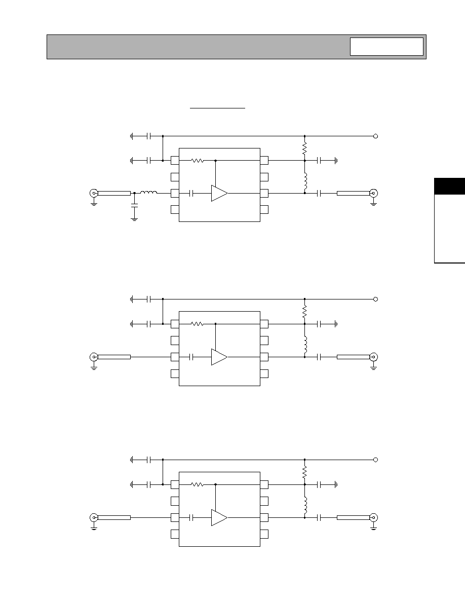
Evaluation Board Schematic (L board)
~900 MHz
(Download Bill of Materials from www.rfmd.com.)
Evaluation Board Schematic (M board)
~1900 MHz
Evaluation Board Schematic (H board)
~2400 MHz
1
2
3
4
8
7
6
5
L1
1 5 nH
C 4
1 .5 pF
C 3
2 2 p F
C 2
22 p F
R 1
0
L 2
8.2 n H
C 1
1 nF
C 5
1 .5 pF
5 0
µ
strip
J 1
R F IN
50
µ
strip
J 2
R F O U T
V C C
2 4 42 40 1 -
1
2
3
4
8
7
6
5
L 1
4.7 n H
C 4
1 .0 pF
C 3
2 2 p F
C 2
22 p F
R 1
0
C 1
1 nF
5 0
µ
strip
J 1
R F IN
50
µ
strip
J 2
R F O U T
V C C
2 44 24 0 0B
1
2
3
4
8
7
6
5
L 1
3.9 n H
C 4
0 .5 pF
C 3
2 2 p F
C 2
22 p F
R 1
0
C 1
1 nF
5 0
µ
strip
J 1
R F IN
50
µ
strip
J 2
R F O U T
V C C
2 4 42 40 2 -

4-236
RF2442
Rev B6 010612
4
G
E
N
E
RA
L
P
URPO
SE
A
M
P
L
IF
IE
RS
Evaluation Board Layout 900MHz
Board Size 1.150" x 1.165"
Evaluation Board Layout 1900MHz
Board Size 1.150" x 1.165"

4-237
RF2442
Rev B6 010612
4
G
E
N
E
RA
L
P
URPO
SE
A
M
P
L
IF
IE
RS
Evaluation Board Layout 2400MHz
Board Size 1.150" x 1.165"

4-238
RF2442
Rev B6 010612
4
G
E
N
E
RA
L
P
URPO
SE
A
M
P
L
IF
IE
RS
Gain vs. Output Level
(Freq = 881MHz)
10
15
20
25
30
-10
-5
0
5
10
15
Output Level (dBm)
Gain
(dB)
Vcc=3.0, Noise Match
Vcc=3.0, Gmax Match
Vcc=3.6, Noise Match
Vcc=3.6, Gmax Match
Input IP3 vs. Input Level
(Freq = 881MHz)
-10
-5
0
5
10
-30
-25
-20
-15
-10
-5
Input Level (dBm)
Input
IP3
(dBm)
Vcc=3.0, Noise Match
Vcc=3.0, Gmax Match
Vcc=3.6, Noise Match
Vcc=3.6, Gmax Match
Noise Figure vs. Frequency
0.0
0.5
1.0
1.5
2.0
2.5
800
850
900
950
1000
Frequency (MHz)
Noise
Figure
(
dB)
Vcc=3.0, Noise Match
Vcc=3.0, Gmax Match
Vcc=3.6, Noise Match
Vcc=3.6, Gmax Match
Output IP3 vs. Output Level
(Freq = 881MHz)
10
15
20
25
30
-10
-5
0
5
10
15
Output Level (dBm)
Output
IP3
(dBm)
Vcc=3.0, Noise Match
Vcc=3.0, Gmax Match
Vcc=3.6, Noise Match
Vcc=3.6, Gmax Match
Output IM3 Level vs. Input Level
(Freq = 881MHz)
-90
-80
-70
-60
-50
-40
-30
-20
-10
0
10
-30
-25
-20
-15
-10
-5
Input Level, per tone (dBm)
Output
IM3
Level,
per
tone
(dBm)
Vcc=3.0, Noise Match
Vcc=3.6, Noise Match
Ideal IM3 Slope
Power Out vs. Power In
(Freq = 881MHz)
-10
-5
0
5
10
15
20
-30
-25
-20
-15
-10
-5
Input Level, single tone (dBm)
Output
Level,
s
ingle
t
one
(dBm)
Vcc = 3.0V
Vcc = 3.6V
Ideal Gain Slope (3.6V)

4-239
RF2442
Rev B6 010612
4
G
E
N
E
RA
L
P
URPO
SE
A
M
P
L
IF
IE
RS
Gain vs. Output Level
(Freq = 1960MHz)
5
10
15
20
-20
-10
0
10
20
Output Level (dBm)
Gain
(dB)
Vcc = 3.6V
Vcc = 3.0V
Input IP3 vs. Input Level
(Freq = 1960MHz)
0
5
10
15
20
-20
-15
-10
-5
0
Input Level (dBm)
Input
IP3
(dBm)
Vcc = 3.6V
Vcc = 3.0V
Noise Figure vs. Frequency
0.0
0.4
0.8
1.2
1.6
2.0
1500
1600
1700
1800
1900
2000
Frequency (MHz)
Noise
Figure
(
dB)
Vcc = 3.6V
Vcc = 3.0V
Output IP3 vs. Input Level
(Freq = 1960MHz)
10
15
20
25
30
-20
-15
-10
-5
0
Input Level (dBm)
Input
IP3
(dBm)
Vcc = 3.6V
Vcc = 3.0V
Icc vs. Output Level
(Freq = 881MHz)
5
10
15
20
25
-10
-5
0
5
10
15
Output Level (dBm)
Icc
(
mA)
Vcc=3.0, Noise Match
Vcc=3.0, Gmax Match
Vcc=3.6, Noise Match
Vcc=3.6, Gmax Match
Efficiency vs. Output Level
(Freq = 881MHz)
0%
5%
10%
15%
20%
25%
30%
35%
40%
45%
50%
-10
-5
0
5
10
15
Output Level (dBm)
Efficiency
(
%)
Vcc=3.0, Noise Match
Vcc=3.0, Gmax Match
Vcc=3.6, Noise Match
Vcc=3.6, Gmax Match

4-240
RF2442
Rev B6 010612
4
G
E
N
E
RA
L
P
URPO
SE
A
M
P
L
IF
IE
RS
Output IM3 Level vs. Input Level
(Freq = 1960MHz)
-80
-70
-60
-50
-40
-30
-20
-10
0
-20
-15
-10
-5
0
Input Level, per tone (dBm)
Output
IM3
Level,
per
tone
(dBm)
Vcc = 3.6V
Vcc = 3.0V
Ideal IM3 Slope
Power Out vs. Power In
(Freq = 1960MHz)
-10
-5
0
5
10
15
20
-20
-15
-10
-5
0
5
10
Input Level, single tone (dBm)
Output
Level,
s
ingle
t
one
(dBm)
Vcc = 3.0V
Vcc = 3.6V
Ideal Gain Slope (3.6V)
Icc vs. Output Level
(Freq = 1960MHz)
5
10
15
20
25
-20
-10
0
10
20
Output Level (dBm)
Icc
(
mA)
Vcc = 3.6V
Vcc = 3.0V
Efficiency vs. Output Level
(Freq = 1960MHz)
0%
10%
20%
30%
40%
50%
60%
70%
-10
-5
0
5
10
15
20
Output Level (dBm)
Efficiency
(
%)
Vcc = 3.0V
Vcc = 3.6V