
8-81
Product Description
Ordering Information
Typical Applications
Features
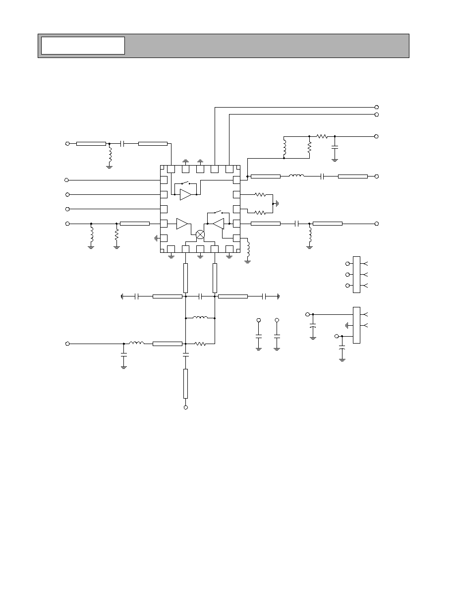
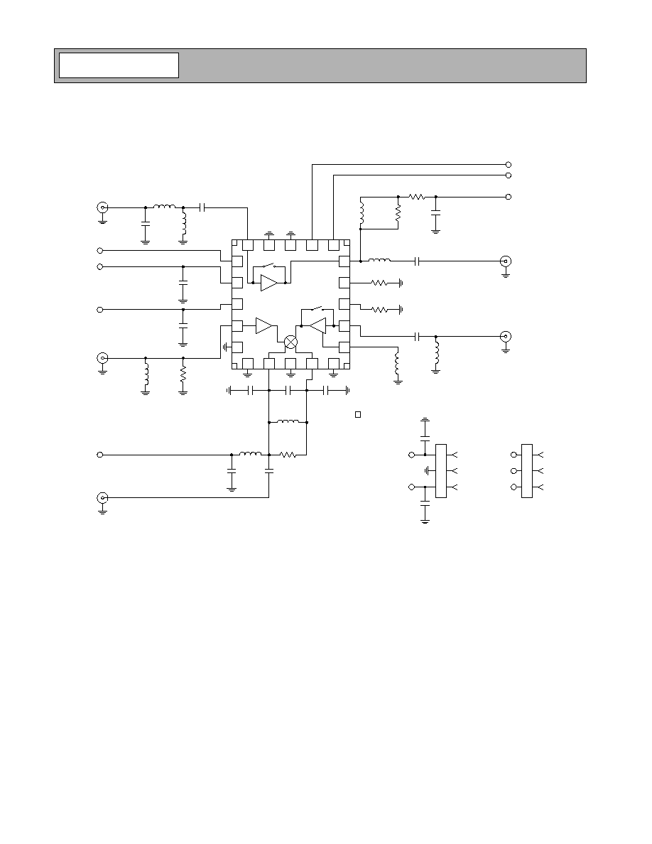
Functional Block Diagram
RF Micro Devices, Inc.
7628 Thorndike Road
Greensboro, NC 27409, USA
Tel (336) 664 1233
Fax (336) 664 0454
http://www.rfmd.com
Optimum Technology MatchingÆ Applied
Si BJT
GaAs MESFET
GaAs HBT
Si Bi-CMOS
SiGe HBT
Si CMOS
InGaP/HBT
GaN HEMT
SiGe Bi-CMOS
19
NC
18
NC
17
LNA GAIN
16
MI
X
GA
I
N
14
ISET1
13
ISET2
12
MIX IN
10
NC
IF
-
9
8
NC
7
IF
+
5
NC
4
LO IN
3
VCC2
2
VCC1
1
ENABLE
*
*
*
*
20
LNA IN
NC
6
11
LNA2 E
15
LNA OUT
*
Represents "GND".
RF2460
PCS CDMA LOW NOISE AMPLIFIER/MIXER
1500MHz TO 2200MHz DOWNCONVERTER
∑ CDMA PCS Handsets
∑ GPS Receiver
∑ W-CDMA Handsets
∑ General Purpose Downconverter
∑ Commercial and Consumer Systems
∑ Portable Battery-Powered Equipment
The RF2460 is a receiver front-end designed for the
receive section of PCS CDMA and W-CDMA applica-
tions. It is designed to amplify and downconvert RF sig-
nals while providing 29dB of stepped gain control range
and features digital control of LNA gain, mixer gain, and
power down mode. A further feature of the chip is adjust-
able IIP3 of the LNA and mixer using an off-chip current
setting resistor. Noise Figure, IP3, and other specs are
designed to be compatible with the IS-98B for CDMA
PCS communications. The IC is manufactured on an
advanced Silicon Germanium Bi-CMOS process and is
assembled in a 20-pin, QFN package with an exposed die
flag.
∑ Complete Receiver Front-End
∑ Stepped LNA/Mixer Gain Control
∑ Adjustable LNA/Mixer Bias Current
∑ 24dB Gain and 2.2dB Noise Figure at
Maximum Cascade Gain
RF2460
PCS CDMA Low Noise Amplifier/Mixer 1500MHz to
2200MHz Downconverter
RF2460 PCBA
Fully Assembled Evaluation Board
0
Rev B3 030425
Dimensions in mm.
Note orientation of package.
12∞
MAX
-C-
0.05
1.00
0.90
0.05 C
0.60
0.24 TYP
0.20
0.10
C A B
M
2
0.65
0.30
4 PLCS
2.10 SQ.
0.23
0.13
4 PLCS
0.50
0.75
0.50
NOTES:
Shaded lead is Pin 1.
1
Dimension applies to plated terminal:
to be measured between 0.02 mm and
0.25 mm from terminal end.
2
0.15 C A
2 PLCS
-A-
4.00
3.75
2 PLCS
0.15 C
4.00
0.15 C B
2 PLCS
-B-
3.75
2 PLCS
0.15 C
Package Style: QFN, 20-Pin, 4x4
!

8-82
RF2460
Rev B3 030425
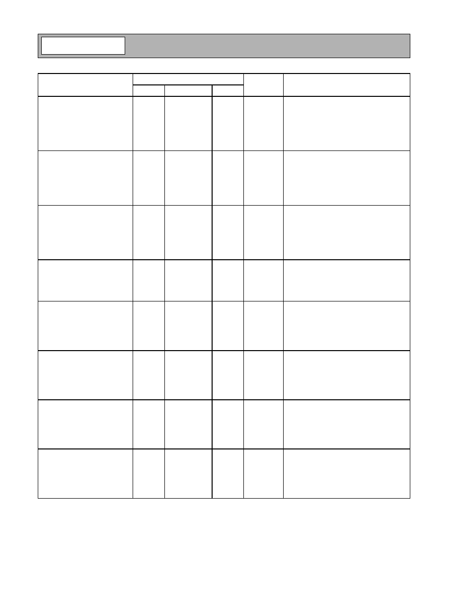
Absolute Maximum Ratings
Parameter
Rating
Unit
Supply Voltage
-0.5 to +5.0
V
DC
Input LO and RF Levels
+6
dBm
Operating Ambient Temperature
-40 to +85
∞C
Storage Temperature
-40 to +150
∞C
Parameter
Specification
Unit
Condition
Min.
Typ.
Max.
Overall
T = 25∞C, V
CC
=2.75V, RF=1.96GHz,
LO=2170MHz@-7dBm, IF=210MHz
RF Frequency Range
1500 to 2200
MHz
LO Frequency Range
1200 to 2600
MHz
IF Frequency Range
0.1 to 250
MHz
Bias Current
2.5
2.8
mA
LNA, mixer and preamp for bias circuitry.
US PCS - LNA
Gain
13.5
15.0
dB
Noise Figure
1.4
1.8
dB
Input IP3
+6.0
+7.0
dBm
IIP3 is adjustable (see plots for setting).
ISET1 (pin 14) external resistor sets current
consumption and performance.
Input VSWR
2:1
Output VSWR
2:1
Current at Input IP3
7
7.5
mA
US PCS - LNA Bypass
Gain
-6
-5
dB
Noise Figure
5
5.5
dB
Input IP3
+23.0
+26.0
dBm
Input VSWR
2:1
Output VSWR
2:1
Current
0
mA
US PCS - Mixer - High Gain
Mode
1k
balanced load.
Gain
10
12
dB
Noise Figure
6.5
7.5
dB
Input IP3
+3.0
+4.0
dBm
IIP3 is adjustable (see plots for setting).
RF to IF Isolation
>45
dB
ISET2 (pin 13) external resistor sets current
consumption and performance.
Input VSWR
2:1
Output VSWR
2:1
Current
12
13
mA
US PCS - Mixer - Low Gain
Mode
1k
balanced load.
Gain
0
1.5
dB
Noise Figure
15
16
dB
Input IP3
+13.0
+14.0
dBm
IIP3 is adjustable
RF to IF Isolation
>45
dB
ISET2 (pin 13) external resistor sets current
consumption and performance.
Input VSWR
2:1
Output VSWR
2:1
Current
7.5
8.0
mA
Caution! ESD sensitive device.
RF Micro Devices believes the furnished information is correct and accurate
at the time of this printing. However, RF Micro Devices reserves the right to
make changes to its products without notice. RF Micro Devices does not
assume responsibility for the use of the described product(s).

8-83
RF2460
Rev B3 030425
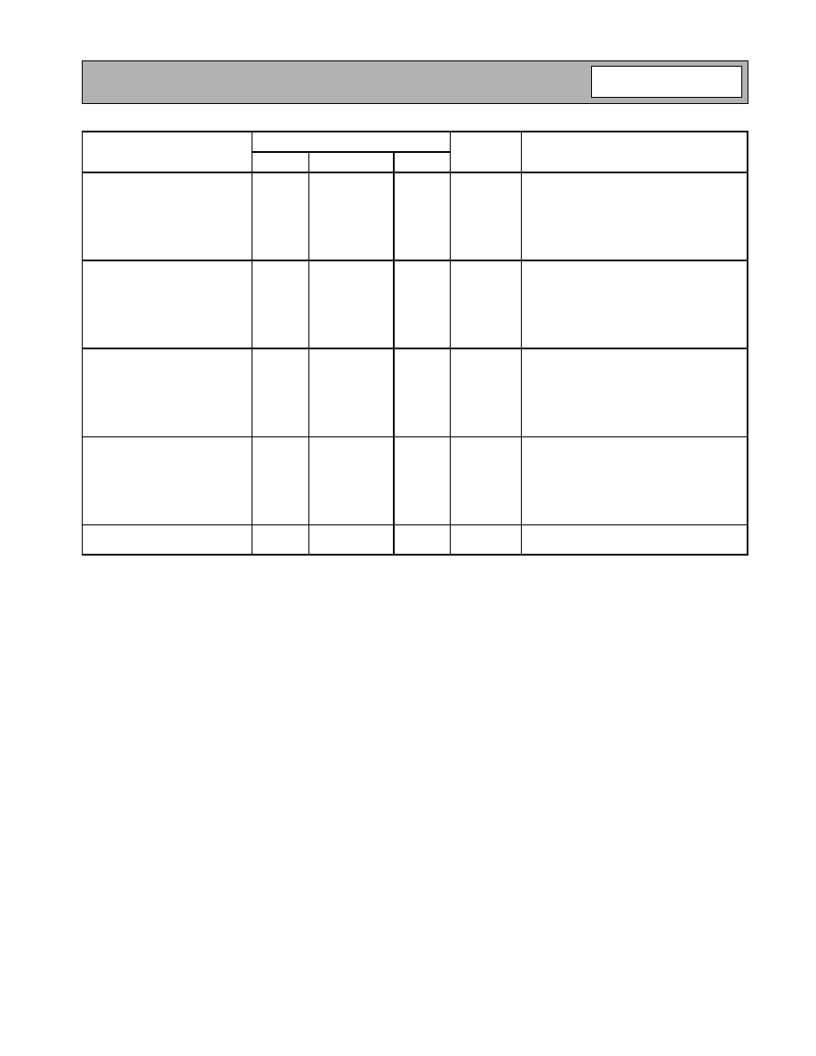
Parameter
Specification
Unit
Condition
Min.
Typ.
Max.
KPCS - LNA
Gain
14.5
16.0
dB
Noise Figure
1.4
1.8
dB
Input IP3
+5.0
+6.0
dBm
IIP3 is adjustable (see plots for setting).
ISET1 (pin 14) external resistor sets current
consumption and performance.
Input VSWR
2:1
Output VSWR
2:1
Current at Input IP3
7
7.5
mA
KPCS - LNA Bypass
Gain
-6
-5
dB
Noise Figure
5.0
5.5
dB
Input IP3
+23.0
+26.0
dBm
Input VSWR
2:1
Output VSWR
2:1
Current
0
mA
KPCS - Mixer - High Gain
Mode
1k
balanced load.
Gain
10
12
dB
Noise Figure
6.5
7.5
dB
Input IP3
+2.5
+3.5
dBm
IIP3 is adjustable (see plots for setting).
RF to IF Isolation
>45
dB
ISET2 (pin 13) external resistor sets current
consumption and performance.
Input VSWR
2:1
Output VSWR
2:1
Current
12
13
mA
KPCS - Mixer - Low Gain
Mode
1k
balanced load.
Gain
0
1.5
dB
Noise Figure
15
16
dB
Input IP3
+13.0
+14.0
dBm
IIP3 is adjustable
RF to IF Isolation
>45
dB
ISET2 (pin 13) external resistor sets current
consumption and performance.
Input VSWR
2:1
Output VSWR
2:1
Current
7.5
8.0
mA
8-84
RF2460
Rev B3 030425
Parameter
Specification
Unit
Condition
Min.
Typ.
Max.
GPS - LNA
Gain
16
dB
Noise Figure
1.4
dB
Input IP3
+7.0
dBm
IIP3 is adjustable. ISET1 (pin 14) external
resistor sets current consumption and per-
formance.
Current at Input IP3
7
mA
GPS - Mixer
Gain
17
dB
Noise Figure
6
dB
Input IP3
-5.0
dBm
IIP3 is adjustable. ISET1 (pin 14) external
resistor sets current consumption and per-
formance.
Current at Input IP3
16
mA
GPS - Cascaded
Gain
31
dB
Noise Figure
1.8
dB
Input IP3
-19.0
dBm
IIP3 is adjustable. ISET1 (pin 14) external
resistor sets current consumption and per-
formance.
Current at Input IP3
23
mA
Local Oscillator Input
Input Level
-10
-7
0
dBm
LO to RF Isolation
>40
dB
Any gain state.
LO to LNA Isolation
>60
dB
Any gain state.
LO Current Buffer
4.5
5.0
mA
I
CC2
when LO signal is present
US PCS - Cascade -
LNA High/Mixer High
LNA High Gain/Mixer High Gain
Assuming 3dB loss of filter
Gain
24
dB
IF 1, 1k
balanced load.
Noise Figure
2.2
dB
Input IP3
-8.0
dBm
Single sideband.
Total Current
26
mA
US PCS - Cascade -
LNA High/Mixer Low
LNA High Gain/Mixer Low Gain
Assuming 3dB loss of filter
Gain
13.5
dB
IF 1, 1k
balanced load.
Noise Figure
5.3
dB
Input IP3
+1.0
dBm
Single sideband.
Total Current
21
mA
US PCS - Cascade -
LNA Low/Mixer High
LNA Low Gain/Mixer High Gain
Assuming 3dB loss of filter
Gain
4
dB
IF 1, 1k
balanced load.
Noise Figure
14.5
dB
Input IP3
+12.0
dB
Single sideband.
Total Current
19
mA
US PCS - Cascade -
LNA Low/Mixer Low
LNA Low Gain/Mixer Low Gain
Assuming 3dB loss of filter
Gain
-6.5
dB
IF 1, 1k
balanced load.
Noise Figure
23
dB
Input IP3
+20.5
dB
Single sideband.
Total Current
14
mA
8-85
RF2460
Rev B3 030425
Parameter
Specification
Unit
Condition
Min.
Typ.
Max.
KPCS - Cascade -
LNA High/Mixer High
LNA High Gain/Mixer High Gain
Assuming 3dB loss of filter
Gain
25
dB
IF 1, 1k
balanced load.
Noise Figure
2.2
dB
Input IP3
-9.5
dBm
Single sideband.
Total Current
26
mA
KPCS - Cascade -
LNA High/Mixer Low
LNA High Gain/Mixer Low Gain
Assuming 3dB loss of filter
Gain
14.5
dB
IF 1, 1k
balanced load.
Noise Figure
5.3
dB
Input IP3
+1.0
dBm
Single sideband.
Total Current
21
mA
KPCS - Cascade -
LNA Low/Mixer High
LNA Low Gain/Mixer High Gain
Assuming 3dB loss of filter
Gain
4
dB
IF 1, 1k
balanced load.
Noise Figure
14.5
dB
Input IP3
+12.0
dB
Single sideband.
Total Current
19
mA
KPCS - Cascade -
LNA Low/Mixer Low
LNA Low Gain/Mixer Low Gain
Assuming 3dB loss of filter
Gain
-6.5
dB
IF 1, 1k
balanced load.
Noise Figure
23
dB
Input IP3
+22
dB
Single sideband.
Total Current
14
mA
Power Supply
Voltage
2.7
3.0
3.3
V

8-86
RF2460
Rev B3 030425
Pin
Function
Description
Interface Schematic
1
ENABLE
Power down pin. A logic "low" turns the part off. A logic "high" (>1.6V)
turns the part on.
2
VCC1
Supply Voltage for the LNA, mixer, bias, and logic circuitry. External RF
and IF bypassing is required. The trace length between the pin and the
bypass capacitors should be minimized. The ground side of the bypass
capacitors should connect immediately to ground plane.
See pin 20.
3
VCC2
Supply Voltage for the LO buffer amplifier. External RF and IF bypass-
ing is required. The trace length between the pin and the bypass
capacitors should be minimized. The ground side of the bypass capaci-
tors should connect immediately to ground plane.
4
LO IN
Mixer LO Input Pin.
5
NC
No connection. For isolation purposes, this pin is connected to the
ground plane.
6
NC
No connection. For isolation purposes, this pin is connected to the
ground plane.
7
IF+
CDMA IF Output pin. This is a balanced output. The internal circuitry, in
conjunction with an external matching/bias inductor to V
CC
, sets the
operating impedance. This inductor is typically incorporated in the
matching network between the output and IF filter. The part is designed
to drive a 1k
load. Because this pin is biased to V
CC
, a DC blocking
capacitor must be used if the IF filter input has a DC path to ground.
See Application Schematic.
8
NC
No connection. For isolation purposes, this pin is connected to the
ground plane.
9
IF-
Same as pin 7, except complementary output.
See pin 6.
10
NC
No connection. For isolation purposes, this pin is connected to the
ground plane.
11
LNA2 E
Emitter for LNA2. Increasing the inductance on this pin will reduce the
mixer gain, increase IP3 and noise figure.
12
MIX IN
Mixer RF Input Pin. This pin is internally DC biased and should be DC
blocked if connected to a device with DC present. External matching
network sets RF and IF impedance for optimum performance.
13
ISET2
This pin is used to set the bias current and IIP3 of the mixer amplifier
using a resistor to ground. See plots for values and current settings.
14
ISET1
This pin is used to set the bias current and IIP3 of the LNA amplifier
using a resistor to ground. See plots for values and current settings.
15
LNA OUT
LNA output pin. Open collector.
See pin 20.
16
MIX GAIN
CMOS compatible signal controlling mixer gain mode. Setting this sig-
nal high places the mixer in the high gain mode. Setting this signal low
places the mixer in low gain mode by bypassing and shutting off the
mixer buffer amplifier current.
17
LNA GAIN
CMOS compatible signal controlling LNA gain mode. Setting this signal
high places the LNA in the high gain mode. Setting this signal low
bypasses the LNA and shuts off the LNA bias current.
18
NC
No connection. For isolation purposes, this pin is connected to the
ground plane.
19
NC
No connection. For isolation purposes, this pin is connected to the
ground plane.
IF1-
IF1+
1.2 pF 1.2 pF
GND2
MIX IN
MIX GAIN
LNA GAIN

8-87
RF2460
Rev B3 030425
Pin
Function
Description
Interface Schematic
20
LNA IN
RF Input pin. This pin is internally matched for optimum noise figure
from a 50
source.
Pkg
Base
GND
Ground connection. The backside of the package should be soldered to
a top side ground pad which is connected to the ground plane with mul-
tiple vias.
LNA OUT
LNA IN
V
CC1

8-88
RF2460
Rev B3 030425
Output Interface Network of the Mixer
L1, C1, C2, and R form a current combiner which per-
forms a differential to single-ended conversion at the IF
frequency and sets the output impedance. In most
cases, the resonance frequency is independent of R
and can be set according to the following equation:
Where C
EQ
is the equivalent stray capacitance and
capacitance looking into pins 7 and 9. An average
value to use for C
EQ
is 2.5pF.
R can then be used to set the output impedance
according to the following equation:
where R
OUT
is the desired output impedance and R
P
is
the parasitic equivalent parallel resistance of L1.
C
2
should first be set to 0 and C1 should be chosen as
high as possible (suggested less than 20pF), while
maintaining an R
P
of L1 that allows for the desired
R
OUT
. If the self-resonant frequencies of the selected
C1 produce unsatisfactory linearity performance, their
values may be reduced and compensated for by
including C2 capacitor with a value chosen to maintain
the desired F
IF
frequency.
L2 and C3 serve dual purposes. L2 serves as an out-
put bias choke, and C3 serves as a series DC block.
In addition, L2 and C3 may be chosen to form an
impedance matching network if the input impedance of
the IF filter is not equal to R
OUT
. Otherwise, L2 is cho-
sen to be large (suggested 120nH) and C3 is chosen
to be large (suggested 22nF) if a DC path to ground is
present in the IF filter, or omitted if the filter is DC
blocked.
f
IF
1
L1
2
------ C
1
2C
2
C
EQ
+
+
(
)
2
-----------------------------------------------------------
=
R
1
4 R
OUT
---------------------
1
R
P
------
≠
1
≠
=

8-89
RF2460
Rev B3 030425
Application Schematic - US PCS
82
7.5 nH
LNA
GAIN
MIX GAIN
C1
C3
R
C1
L2
0.1
µ
F
0.1
µ
F
47 nH
9.1 k
18 k
2 nH
19 nH
510
10
0.1
µ
F
19
18
17
16
14
13
12
10
9
8
7
5
4
3
2
1
*
*
*
*
20
6
11
15
L1
C2
1 nH
10 nH
22 pF
ENABL
E
LO IN
V
CC
2
V
CC
1
C3
0.1
µ
F
VCC1
C4
0.1
µ
F
VCC2
C3 and C4 should be placed as
closely as possible to pins 2 and 3
V
CC
1
IF OUT
MIX IN
LNA OUT
V
CC
1
0.1
µ
F
LNA IN
4.7 k
10 k
4.7 k
4.7 k
R (
)
110
180
120
110
L2 (nH)
82
120
82
82
L1 (nH)
6
6.2
7
6
C3 (pF)
3
DNI
2
3
C2 (pF)
8
8.2
3.6
4
C1 (pF)
US PCS, IF = 184 MHz
GPS, IF = 184 MHz
Korean PCS, IF = 220 MHz
US PCS, IF = 210 MHz
*
Represents "GND".
8-90
RF2460
Rev B3 030425
Application Schematic - W-CDMA
(See W-CDMA charts for lab measurements at the end of the data sheet)
19
18
17
16
14
13
12
10
9
8
7
5
4
3
2
1
*
*
*
*
20
6
11
15
ENABLE
VCC1
VCC2
50
µ
strip
R1
82
L2
7.5 nH
50
µ
strip
50
µ
strip
C7
4.3 pF
C8
4.3 pF
50
µ
strip
50
µ
strip
C9
4.3 pF
L4
82 nH
R2
DNI
50
µ
strip
L3
150 nH
C5
0.1
µ
F
VCC1
C6
5.6 pF
50
µ
strip
L5
1.0 nH
50
µ
strip
C10
0.1
µ
F
50
µ
strip
L6
47 nH
R3
9.1 k
R6
18 k
50
µ
strip
L7
2.0 nH
C11
22 pF
50
µ
strip
L8
19 nH
R4
510
R5
10
C12
0.1
µ
F
VCC1
MIX_GAIN
LNA_GAIN
50
µ
strip
C2
0.1
µ
F
50
µ
strip
L1
10 nH
RF2460PCBA-U WCDMA
RF @ 2.14 GHz, LO @ 2.33 GHz, IF @ 190 MHz
IF=190 MHz
C3
0.1
µ
F
VCC1
C4
0.1
µ
F
VCC2
C2 and C3 should be placed as
closely as possible to pins 2 and 3
P1
1
2
3
CON3
P1-1
VCC1
GND
C1
1
µ
F
+
P1-3
C13
1
µ
F
+
LO IN
LNA IN
LNA OUT
MIX IN
IF OUT
P2
1
2
3
CON3
P2-1
ENABLE
LNA_GAIN
P2-3
MIX_GAIN
P2-1

8-91
RF2460
Rev B3 030425
Application Schematic - GPS
RF=1575MHz, IF=184MHz, LO=1759MHz
ENABLE
50
µ
strip
68
LNA GAIN
MIX GAIN
50
µ
strip
50
µ
strip
8.2 pF
6.2 pF
50
µ
strip
50
µ
strip
50
µ
strip
8.2 pF
180 nH
50
µ
strip
0.1 uF
***323 pS electrical delay***
***0.03 dB line loss***
50
µ
strip
0.1 uF
50
µ
strip
50
µ
strip
47 nH
***397 pS electrical delay***
***0.26 dB line loss***
13 k
18 k
50
µ
strip
1.2 nH
33 nF
50
µ
strip
***359 pS electrical delay***
***0.23 dB line loss***
12 nH
5
50
µ
strip
47 nF
50
µ
strip
12 nH
50
µ
strip
***C2 & C3 should be placed as
close as possible to pins 2 & 3***
***390 pS electrical delay***
***0.28 dB line loss***
***439 pS electrical delay***
***0.33 dB line loss***
19
18
17
16
14
13
12
10
9
8
7
5
4
3
2
1
*
*
*
*
20
6
11
15
*
Represents "GND".
120 nH
10 k
VCC1
VCC2
IF OUT
V
CC1
LO IN
LNA IN
V
CC1
LNA OUT
MIX IN
0.1 uF
8-92
RF2460
Rev B3 030425
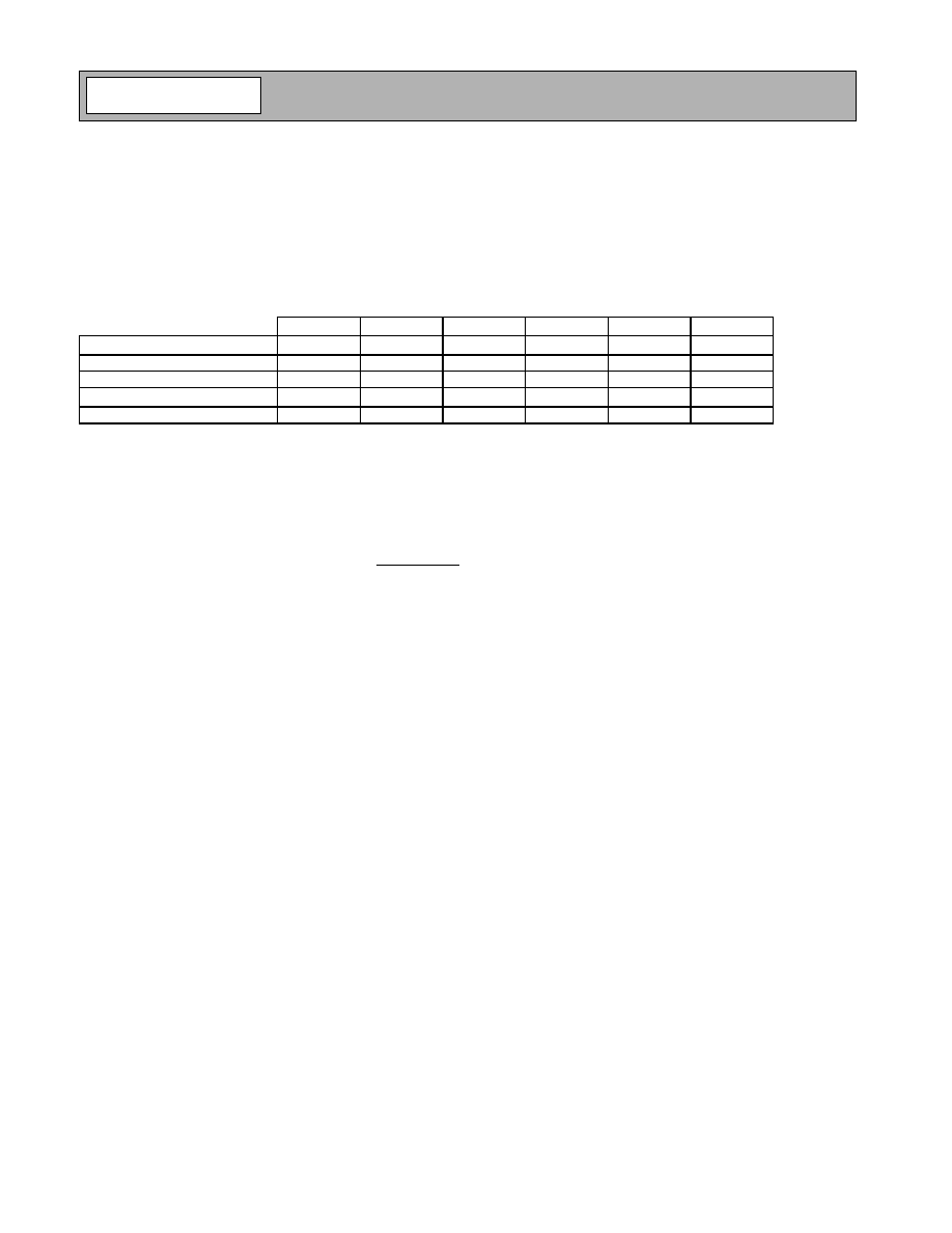
Current Measurement
To measure only the current of the different circuitry in the evaluation board, use the following procedure.
First, replace the bias choke inductor at the output of the mixer (L3 for US-PCS) with a 1
resistor. The voltage across
the resistor will represent the mixer current. Terminate all SMA connections at 50
.
Second, follow the table below.
Therefore
,
CONDITION
Current (mA)
V
CC1
V
CC2
EN
LNA Gain
Mix Gain
I
CC
Total
25.82
1
1
1
1
1
LNA Off
18.77
1
1
1
0
1
Mixer Preamp Off
14.28
1
1
1
0
0
V
CC2
Off
10.05
1
0
1
0
0
Mixer Current
7.72
1
0
1
0
0
LNA (Bypass) = (Computer Simulation) =
0mA
LNA (High Gain) =
25.82-18.77
=
7.05mA
Mixer (Preamp) =
18.77-14.28
=
4.49mA
Mixer =
(Measured)
=
7.70mA
Bias =
10.05-7.7
=
2.35mA
LO Circuitry (V
CC2
) =
14.28-10.05
=
4.23mA
25.82mA

8-93
RF2460
Rev B3 030425
Evaluation Board Schematic
US-PCS, IF=210MHz
(Download Bill of Materials from www.rfmd.com.)
ENABLE
R1
82
L2
7.5 nH
J2
LO IN
LNA GAIN
MIX GAIN
C7
4 pF
C6
6 pF
J3
IF OUT
R2
4.7 k
C9
4 pF
L3
110 nH
VCC1
C5
0.1
µ
F
***323 pS electrical delay***
***0.03 dB line loss***
C10
0.1
µ
F
L6
47 nH
J4
MIX IN
***397 pS electrical delay***
***0.26 dB line loss***
R3
9.1 k
R6
18 k
L7
2 nH
J5
LNA OUT
***359 pS electrical delay***
***0.23 dB line loss***
L8
19 nH
R4
510
R5
10
C12
0.1
µ
F
VCC1
C2
0.1
µ
F
J1
LNA IN
***C3 and C4 should be placed as
close as possible to pins 2 and 3***
***390 pS electrical delay***
***0.28 dB line loss***
***439 pS electrical delay***
***0.33 dB line loss***
19
18
17
16
14
13
12
10
9
8
7
5
4
3
2
1
*
*
*
*
20
6
11
15
* Represents "GND".
P2
1
2
3
CON3
P2-3
MIX GAIN
P2-2
LNA GAIN
P2-1
ENABLE
L4
82 nH
C8
3 pF
P1
1
2
3
CON3
GND
P1-1
C1
0.1
µ
F
VCC1
P1-3
C13
0.1
µ
F
VCC2
VCC1
VCC1
L5
1 nH
C3
0.1
µ
F
C4
0.1
µ
F
L1
10 nH
C11
22 pF
8-94
RF2460
Rev B3 030425
Evaluation Board Schematic
Korean-PCS, IF=220MHz
ENABLE
R1
68
L3
9 nH
J2
LO IN
LNA GAIN
MIX GAIN
C8
3.6 pF
C7
7 pF
J3
IF OUT
R2
4.7 k
C10
3.6 pF
L4
120 nH
VCC1
C6
0.1
µ
F
***291 pS electrical delay***
***0.05 dB line loss***
C11
0.1
µ
F
L7
47 nH
J4
MIX IN
***399 pS electrical delay***
***0.32 dB line loss***
R3
7.5 k
R6
24 k
L8
2.2 nH
J5
LNA OUT
***358 pS electrical delay***
***0.26 dB line loss***
L9
8.2 nH
R4
510
R5
20
VCC1
C3
0.1
µ
F
J1
LNA IN
***C4 and C5 should be placed as
close as possible to pins 2 and 3***
***396 pS electrical delay***
***0.30 dB line loss***
***400 pS electrical delay***
***0.30 dB line loss***
19
18
17
16
14
13
12
10
9
8
7
5
4
3
2
1
*
*
*
*
20
6
11
15
* Represents "GND".
P2
1
2
3
CON3
P2-3
MIX GAIN
P2-2
LNA GAIN
P2-1
ENABLE
L5
82 nH
C9
2 pF
P1
1
2
3
CON3
GND
P1-1
C1
0.1
µ
F
VCC1
P1-3
C14
0.1
µ
F
VCC2
VCC1
VCC1
L6
1 nH
L1
1.6 nH
L2
10 nH
C2
1 pF
C4
0.1
µ
F
C5
0.1
µ
F
C12
22 pF
C13
0.1
µ
F
2460310, Rev. 5

8-95
RF2460
Rev B3 030425
Evaluation Board Layout - US PCS
Board Size 2.0" x 2.0"
Board Thickness 0.034", Board Material FR-4, Multi-Layer
Assembly
Top
Power Plane 1
Power Plane 2

8-96
RF2460
Rev B3 030425
Back

8-97
RF2460
Rev B3 030425
Evaluation Board Layout - Korean PCS
Assembly
Top
Power Plane 1
Power Plane 2
Back

8-98
RF2460
Rev B3 030425
Special Instructions (Board loss, taking into consideration description in the schematic)
LNA
V
CC1
=V
CC2
=Enable=2.75V; Mix Gain=0.0V
To measure I
CC
LNA only:
LNA Gain was switched between 0V and 2.75V, and record the delta current.
Mixer
V
CC1
=V
CC2
=Enable=Mix Gain=2.75V; LNA Gain=0.0V
To measure I
CC
Mixer (LNA should be in bypass mode and LO signal should be present):
Mixer Current=Total IC Current-LO Circuitry (~4.23mA) (See "Current Measurement" section for more details)
V
CC2
only affects LO current buffer and R6 doesn't affect the mixer current.
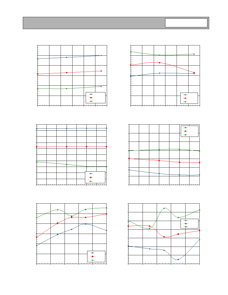
LNA Gain, Noise Figure and IIP3 versus ICC - LNA Only
(LNA High Gain)
0.0
2.0
4.0
6.0
8.0
10.0
12.0
14.0
16.0
18.0
1.0
3.0
5.0
7.0
9.0
11.0
13.0
15.0
X Axis Label (units)
Y Axis Label (units)
-15.0
-10.0
-5.0
0.0
5.0
10.0
15.0
IIP3 (dBm)
Gain (dB)
NF (dB)
IIP3 (dBm)
Mixer Gain, Noise Figure and IIP3 versus I
CC
- Mixer
(Mixer High Gain, LO = -7 dBm)
-20.0
-15.0
-10.0
-5.0
0.0
5.0
10.0
15.0
20.0
25.0
2.0
4.0
6.0
8.0
10.0
12.0
14.0
16.0
18.0
I
CC
(mA)
Gain and Noise Figure (dB)
-15.0
-10.0
-5.0
0.0
5.0
10.0
IIP3 (dBm)
Gain (dB)
NF (dB)
IIP3 (dBm)
Resistor (R6) versus I
CC
(mA) - LNA Only
(LNA High Gain)
0.0
20.0
40.0
60.0
80.0
100.0
120.0
140.0
160.0
180.0
200.0
1.0
3.0
5.0
7.0
9.0
11.0
13.0
15.0
I
CC
(mA)
Resistor R6 (k
)
Resistor (R3) versus I
CC
- Mixer
(Mixer High Gain, LO = 2170 @ -7 dBm)
0.0
20.0
40.0
60.0
80.0
100.0
120.0
140.0
160.0
180.0
2.0
4.0
6.0
8.0
10.0
12.0
14.0
16.0
18.0
I
CC
(mA)
Resistor R3 (k
)
US-PCS

8-99
RF2460
Rev B3 030425
Instructions (Board loss, taking into consideration description in the W-CDMA schematic)
LNA
I
CC
LNA current=total current (V
CC
=LNA Gain=2.75)-total current (V
CC
=2.75; LNA Gain=0)
To measure I
CC
LNA only:
LNA Gain was switched between 0V and 2.75V, and record the delta current.
Mixer
I
CC
Mix and Bias Current=Total Current (V
CC1
=EN=V
CC2
=Mix Gain=2.75; LNA Gain=0)-total current (V
CC1
=EN=2.75;
Mix Gain=LNA Gain=V
CC2
=0)
LO signal should be present. V
CC2
only affects LO current buffer and R6 doesn't affect the mixer current.
LNA Gain, Noise Figure, and IIP3 versus I
CC
- LNA Only
(LNA High Gain)
-10.00
-5.00
0.00
5.00
10.00
15.00
20.00
1.00
3.00
5.00
7.00
9.00
11.00
13.00
15.00
I
CC
(mA)
Gain (dB) and IIP3 (dBm)
0.00
0.20
0.40
0.60
0.80
1.00
1.20
1.40
1.60
1.80
2.00
Noise Figure (dB)
Gain (dB)
IIP3 (dBm)
NF (dBm)
Mixer Gain, Noise Figure and IIP3 versus I
CC
- Mixer and
Bias Circuits
(Mixer High Gain, LO=-7dBm)
-8.00
-6.00
-4.00
-2.00
0.00
2.00
4.00
6.00
8.00
10.00
12.00
14.00
6.00
6.50
7.00
7.50
8.00
8.50
9.00
9.50
10.00
I
CC
(mA)
Gain (dB) and IIP3 (dBm)
0.00
2.00
4.00
6.00
8.00
10.00
12.00
Noise Figure (dB)
Gain (dB)
IIP3 (dBm)
NF (dBm)
R6 versus I
CC
for LNA
0.0
10.0
20.0
30.0
40.0
50.0
60.0
70.0
80.0
90.0
1.0
3.0
5.0
7.0
9.0
11.0
13.0
15.0
I
CC
(mA)
R6 (mA)
R3 versus I
CC
for Mixer and Bias Circuits
0.0
5.0
10.0
15.0
20.0
25.0
30.0
35.0
40.0
6.0
6.5
7.0
7.5
8.0
8.5
9.0
9.5
10.0
I
CC
(mA)
R3 (k
)
W-CDMA
(See W-CDMA Application Schematic)

8-100
RF2460
Rev B3 030425
By using a R6=39k
and R3=24k
, the following results were obtained. RF=2140MHz, LO=2330MHz, IF=190MHz.
LNA (High Gain Mode) WCDMA
12.00
12.20
12.40
12.60
12.80
13.00
13.20
13.40
13.60
13.80
14.00
2.75
2.85
2.95
3.05
3.15
3.25
V
CC
(V)
Gain (dB)
Gain, -30∫
Gain, 25∫
Gain, 85∫
LNA (High Gain Mode) W-CDMA
4.00
5.00
6.00
7.00
8.00
9.00
10.00
2.75
2.85
2.95
3.05
3.15
3.25
3.35
V
CC
(V)
IIP3 (dBm)
IIP3, -30∫
IIP3, 25∫
IIP3, 85∫
LNA (High Gain Mode) W-CDMA
0.00
0.50
1.00
1.50
2.00
2.50
2.75
2.85
2.95
3.05
3.15
3.25
3.35
V
CC
(V)
Noise Figure (dB)
NF, -30∫
NF, 25∫
NF, 85∫
LNA Current W-CDMA
3.90
3.95
4.00
4.05
4.10
4.15
4.20
4.25
4.30
4.35
2.75
2.85
2.95
3.05
3.15
3.25
3.35
V
CC
(V)
I
CC
(mA)
Icc, -30∫
Icc, 25∫
Icc, 85∫
8-101
RF2460
Rev B3 030425
Mixer High Gain Mode,
LO @ -7 dBm W-CDMA
8.00
9.00
10.00
11.00
12.00
13.00
14.00
2.75
2.85
2.95
3.05
3.15
3.25
3.35
V
CC
(V)
Gain (dB)
Gain, -30∫
Gain, 25∫
Gain, 85∫
Mixer High Gain Mode,
LO @ -7 dBm W-CDMA
8.00
8.50
9.00
9.50
10.00
10.50
11.00
2.75
2.85
2.95
3.05
3.15
3.25
3.35
V
CC
(V)
Noise Figure (dB)
NF, -30∫
NF, 25∫
NF, 85∫
Mixer High Gain Mode,
V
CC
@ 2.75 W-CDMA
8.0
8.5
9.0
9.5
10.0
10.5
11.0
11.5
12.0
12.5
13.0
-10.0
-9.0
-8.0
-7.0
-6.0
-5.0
-4.0
-3.0
LO (dBm)
Gain (dB)
Gain, -30∫
Gain, 25∫
Gain, 85∫
Mixer IF High Gain Mode,
V
CC
@ 2.75 W-CDMA
-3.5
-3.0
-2.5
-2.0
-1.5
-1.0
-0.5
0.0
-10.0
-9.0
-8.0
-7.0
-6.0
-5.0
-4.0
-3.0
LO (dBm)
IIP3 (dBm)
IIP3, -30∫
IIP3, 25∫
IIP3, 85∫
Mixer IF High Gain Mode,
V
CC
@ 2.75 W-CDMA
8.0
8.5
9.0
9.5
10.0
10.5
11.0
-10.0
-8.0
-6.0
-4.0
-2.0
0.0
LO (dBm)
Noise Figure (dB)
NF, -30∫
NF, 25∫
NF, 85∫
Mixer IF High Gain Mode,
V
CC
@ 2.75 W-CDMA
5.5
5.6
5.7
5.8
5.9
6.0
6.1
6.2
-10.0
-8.0
-6.0
-4.0
-2.0
0.0
LO (dBm)
I
CC
Mixer and Bias Current (mA)
Icc, -30∫
Icc, 25∫
Icc, 85∫
8-102
RF2460
Rev B3 030425
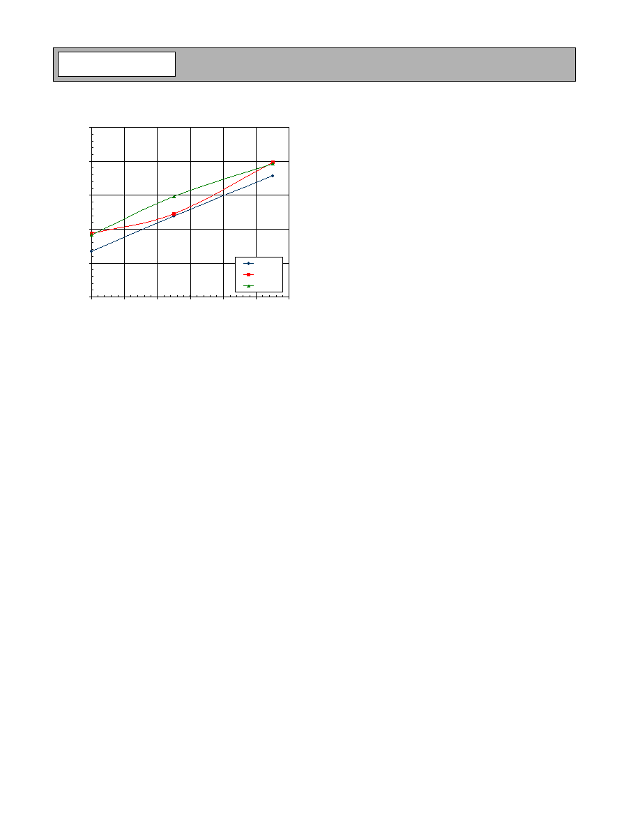
Mixer IF High Gain Mode,
LO @ -7 dBm W-CDMA
5.00
5.50
6.00
6.50
7.00
7.50
2.75
2.85
2.95
3.05
3.15
3.25
3.35
V
CC
(V)
I
CC
Mixer and Bias Circuit (mA)
Icc, -30∫
Icc, 25∫
Icc, 85∫