 | –≠–ª–µ–∫—Ç—Ä–æ–Ω–Ω—ã–π –∫–æ–º–ø–æ–Ω–µ–Ω—Ç: RF2469 | –°–∫–∞—á–∞—Ç—å:  PDF PDF  ZIP ZIP |
¸
8-33
8
F
R
O
N
T
-
E
NDS
Preliminary
Product Description
Ordering Information
Typical Applications
Features
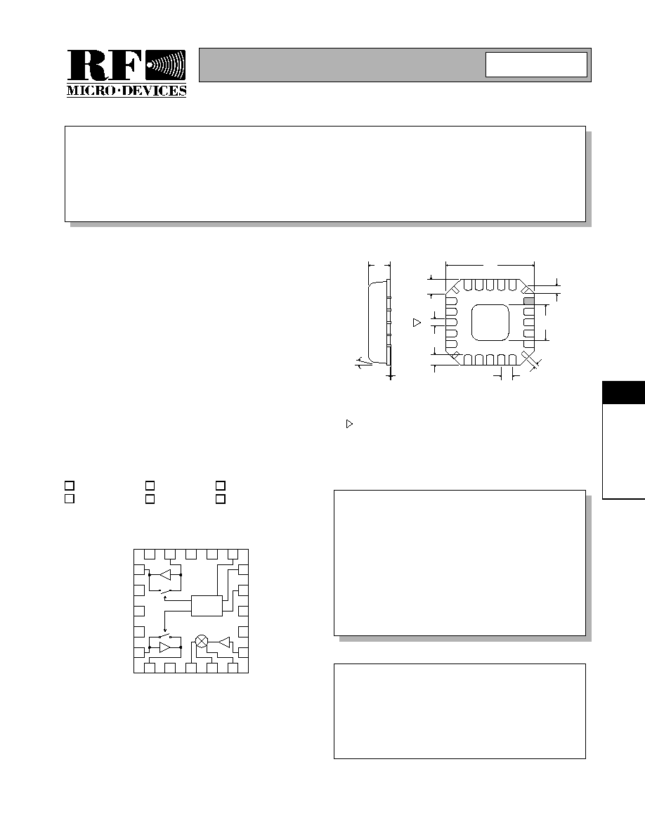
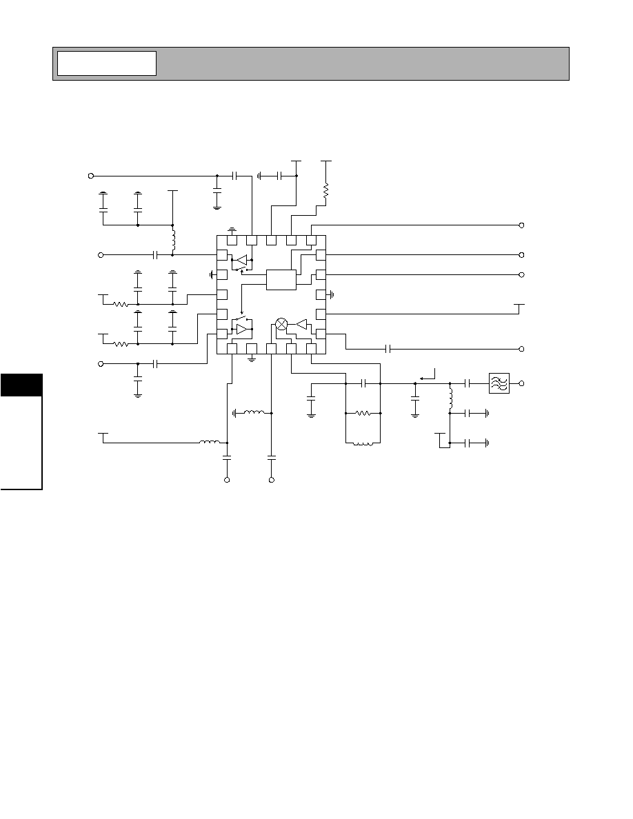
Functional Block Diagram
RF Micro Devices, Inc.
7628 Thorndike Road
Greensboro, NC 27409, USA
Tel (336) 664 1233
Fax (336) 664 0454
http://www.rfmd.com
Optimum Technology MatchingÆ Applied
Si BJT
GaAs MESFET
GaAs HBT
Si Bi-CMOS
SiGe HBT
Si CMOS
19
LNA1
IN
18
VCC1
17
VCC1
16
ENABLE
14
LNA2
BYP
13
GND
12
VCC1
10
IF-
IF+
9
8
MI
X
I
N
7
GND
5
LNA2 IN
4
VCC1
3
VCC1
2
GND
1
LNA1 OUT
20
GND
LNA2
OUT
6
11
LO IN
15
LNA1 BYP
Logic
Control
RF2469
W-CDMA AND PCS LOW NOISE
AMPLIFIER/MIXER DOWNCONVERTER
∑ W-CDMA Handsets
∑ PCS Handsets
∑ General Purpose Downconverter
∑ Commercial and Consumer Systems
∑ Portable Battery-Powered Equipment
The RF2469 is a receiver front-end designed for the
receive section of W-CDMA and PCS applications. It is
designed to amplify and downconvert RF signals while
providing 23dB of stepped gain control range and fea-
tures digital control of the LNA gain and mixer gain. A fur-
ther feature of the chip is adjustable IIP3 of the LNA and
mixer using an off-chip current setting resistor. Noise Fig-
ure, IP3, and other specs are designed to be compatible
with W-CDMA and PCS communications. The IC is man-
ufactured on an advanced Gallium Arsenide Heterojunc-
tion
Bipolar
Transistor
(GaAs
HBT)
process
and
packaged in a 20-pin, leadless chip carrier with an
exposed die flag.
∑ Complete Receiver Front-End
∑ Stepped LNA/Mixer Gain Control
∑ Adjustable LNA/Mixer Bias Current
∑ 23dB Maximum Cascade Gain
∑ 2.5dB Noise Figure at Maximum
Cascade Gain
RF2469
W-CDMA and PCS Low Noise Amplifier/Mixer Down-
converter
RF2469 PCBA
Fully Assembled Evaluation Board
8
Rev A5 010717
1.00
0.90
4.00
sq.
0.60
0.24 typ
3
0.20
0.75
0.50
0.23
0.13
4 PLCS
0.50
2.10
sq.
0.65
0.30
4 PLCS
0.05
12∞
MAX
Dimensions in mm.
Note orientation of package.
NOTES:
Package Warpage: 0.05 mm max.
4
Die Thickness Allowable: 0.305 mm max.
5
Pin 1 identifier must exist on top surface of package by identification
mark or feature on the package body. Exact shape and size is optional.
2
Shaded lead is Pin 1.
1
Dimension applies to plated terminal: to be measured between 0.02 mm
and 0.25 mm from terminal end.
3
Package Style: LCC, 20-Pin, 4x4
Preliminary
8-34
RF2469
Rev A5 010717
8
F
R
O
N
T
-
E
NDS
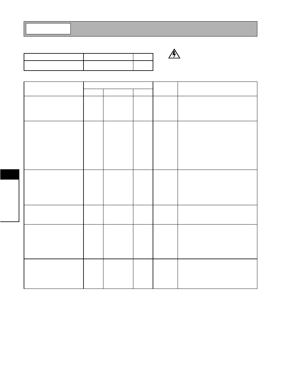
Absolute Maximum Ratings
Parameter
Rating
Unit
Operating Ambient Temperature
-40 to +85
∞C
Storage Temperature
-40 to +150
∞C
Parameter
Specification
Unit
Condition
Min.
Typ.
Max.
Overall
T = 25∞C, V
CC
= 2.78V, RF= 2140MHz,
LO= 2330MHz @ -10dBm
RF Frequency Range
2110 to 2170
MHz
LO Frequency Range
2300 to 2360
MHz
IF Frequency Range
190
MHz
LNA 1
1st LNA current setting resistor (R1) is
1.1k
. 1st LNA current and IIP3 are adjust-
able via R1.
Gain
9
10
11
dB
Noise Figure
1.45
1.6
dB
Input IP3
+7.0
+10.0
dBm
Input VSWR
<2:1
Output VSWR
<2:1
P1dB
-3
dB
See LNA P1dB Compression Point section.
Current
4.5
mA
LNA 1 Bypass
Gain
-5
-2
0
dB
Noise Figure
2
2.4
dB
Input IP3
+20.0
+25.0
dBm
Input VSWR
<2:1
Output VSWR
<2:1
Current
1.6
mA
Local Oscillator Input
Single-ended.
Optimum LO Drive -10dBm to -5dBm.
Input Level
-10
dBm
LO to IF Isolation
+38
dB
Mixer/LNA2 BYP High
T = 25∞C, V
CC
= 2.78V, RF= 2140MHz,
LO= 2330MHz@-10dBm, LNA2BYP = 1,
EN= 1
Gain
15
17
dB
Noise Figure
4.5
dB
Input IP3
-7.0
-3.0
dBm
LNA 2 current setting resistor (R2) is 2.4k
Input IP2
+11.0
+14.0
dBm
LNA 2 current and IIP3 are adjustable via R2
Mixer/LNA2 BYP Low
T = 25∞C, V
CC
= 2.78V, RF= 2140MHz,
LNA2BYP= 0, EN =1
Gain
4
6
dB
Noise Figure
10.5
dB
Input IP3
+2.0
+4.0
dBm
LNA 2 current setting resistor (R2) is 2.4k
Input IP2
+19.0
+22.0
dBm
LNA 2 current and IIP3 are adjustable via R2
Caution! ESD sensitive device.
RF Micro Devices believes the furnished information is correct and accurate
at the time of this printing. However, RF Micro Devices reserves the right to
make changes to its products without notice. RF Micro Devices does not
assume responsibility for the use of the described product(s).
Preliminary
8-35
RF2469
Rev A5 010717
8
F
R
O
N
T
-
E
NDS
Parameter
Specification
Unit
Condition
Min.
Typ.
Max.
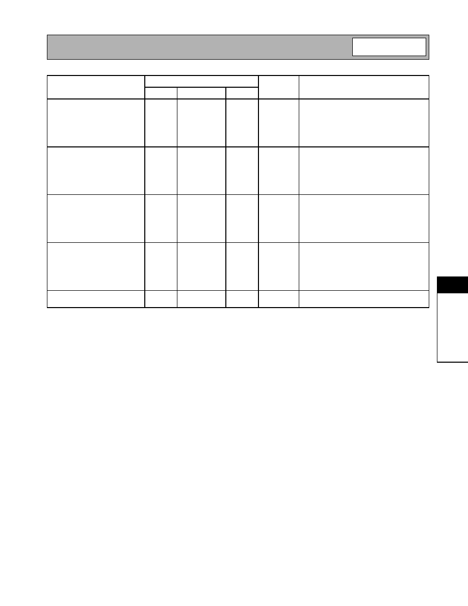
Cascade - Condition 1
LNA1 BYP high, LNA2 BYP high,
ENABLE high. Assuming 2.5dB filter loss.
Gain
24.5
dB
Noise Figure
2.55
dB
Input IP3
-10.5
dBm
Current Consumption*
18.6
23
mA
Cascade - Condition 2
LNA1 BYP high, LNA2 BYP low,
ENABLE high. Assuming 2.5dB filter loss.
Gain
13.5
dB
Noise Figure
5.2
dB
Input IP3
-3.5
dBm
Current Consumption*
17
17.5
mA
Cascade - Condition 3
LNA1 BYP low, LNA2 BYP high,
ENABLE high. Assuming 2.5dB filter loss.
Gain
12.5
dB
Noise Figure
9
dB
Input IP3
+1.4
dBm
Current Consumption*
14
15
mA
Cascade - Condition 4
LNA1 BYP low, LNA2 BYP low,
ENABLE High. Assuming 2.5dB filter loss.
Gain
1.50
dB
Noise Figure
15
dB
Input IP3
+8.2
dBm
Current Consumption*
12.5
13.5
mA
Power Supply
Voltage
2.7
2.75
3.3
V
*RF2469 is a very flexible device. Customers may choose different current consumption (see Low Current Configuration section).
Preliminary
8-36
RF2469
Rev A5 010717
8
F
R
O
N
T
-
E
NDS
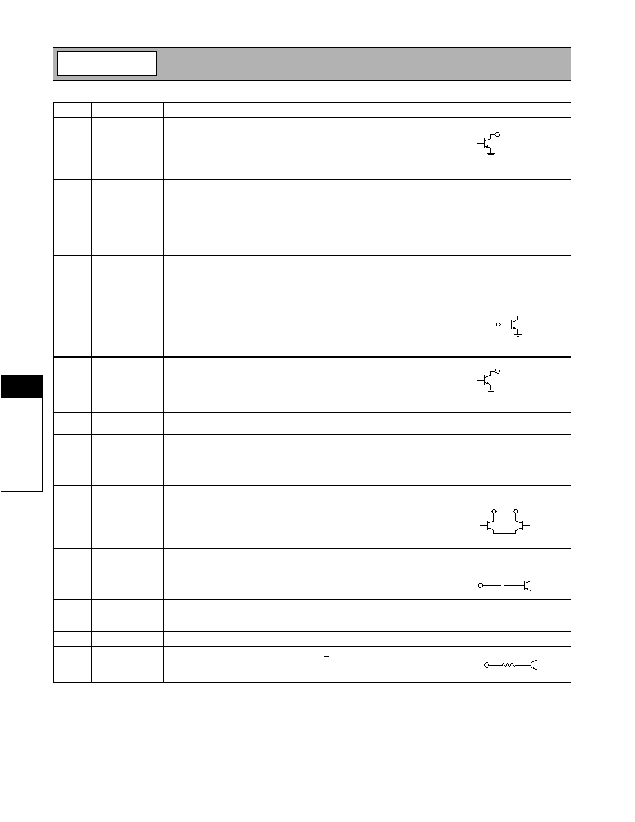
Pin
Function
Description
Interface Schematic
1
LNA1 OUT
LNA output pin. This is an open-collector output. Externally matched to
50
.
2
GND
This pin is connected to the ground plane.
3
VCC1
Supply voltage for LNA1. An external resistor is placed in series with
this pin to adjust the current and IIP3 of LNA1. A nominal value of
1.1k
sets the LNA1 current to 4.5mA with a minimum IIP3 of +7dBm.
External RF bypassing is required. The trace length between the
bypass caps and the pin should be minimized. Connect ground sides of
caps directly to ground.
4
VCC1
Supply voltage for LNA2. An external resistor is placed in series with
this pin to adjust the current and IIP3 of LNA2. A nominal value of
2.4k
sets the LNA2 current to 1.6mA. External RF bypassing is
required. The trace length between the bypass caps and the pin should
be minimized. Connect ground sides of caps directly to ground.
5
LNA2 IN
RF input to LNA2. This pin is internally DC-biased and, if it is con-
nected to a device with DC present, should be DC-blocked with a
capacitor suitable for the frequency of operation.
6
LNA2 OUT
LNA output pin. This is an open-collector output. In normal operation,
this pin is externally cascaded with pin 8 (MIX IN).
7
GND
Ground connection. For best performance, keep traces physically short
and connect directly to ground plane.
8
MIX IN
Mixer RF input pin. This pin requires a DC path to ground. In normal
operation, this pin is externally cascaded with pin 6 (LNA2 OUT). The
external match ensures a conjugate match between pin 6 and pin 8
while providing a DC path to ground for pin 8 and a DC-block between
pin 8 and pin 6.
9
IF+
IF output pin. The output is balanced. A current combiner external net-
work performs a differential to single-ended conversion and sets the
output impedance. There must be a DC path from V
CC
to this pin. This
is normally achieved with the current combiner network. A DC blocking
cap must be present if the IF filter input has a DC path to ground.
10
IF-
Same as pin 9, except complementary output.
See pin 9.
11
LO IN
Mixer LO single-ended input. The pin is internally DC-blocked. External
matching sets impedance.
12
VCC1
Supply voltage for LO buffer. External RF bypassing is required. The
trace length between the bypass caps and the pin should be minimized.
Connect ground sides of caps directly to ground.
13
GND
This pin is connected to the ground plane.
14
LNA2 BYP
Logic control for LNA2 gain. A logic high (>2.4V) places LNA2 in the
high gain mode. A logic low (<0.3V) place LNA2 in the bypass mode.
LNA1 OUT
LNA2 IN
LNA2 OUT
IF+
IF-
LO IN
LNA2 BYP
32 k

Preliminary
8-37
RF2469
Rev A5 010717
8
F
R
O
N
T
-
E
NDS
Pin
Function
Description
Interface Schematic
15
LNA1 BYP
Logic control for LNA1 gain. A logic high (>2.4V) places LNA1 in the
high gain mode. A logic low (<0.3V) place LNA1 in the bypass mode.
16
ENABLE
A logic control for mixer and LO buffer. A logic high (>2.4V) turn the
mixer and LO buffer on. A logic low (<0.3V) disable the mixer and LO
buffer.
17
VCC1
Supply voltage for the mixer. An external resistor is place in series with
this pin to adjust the mixer current. A nominal value of 1000
set the
mixer current to ~10mA. External RF bypassing is required. The trace
length between the bypass caps and the pin should be minimized. Con-
nect ground sides of caps directly to ground.
18
VCC1
Supply voltage for IC. External RF bypassing is required. The trace
length between the bypass caps and the pin should be minimized. Con-
nect ground sides of caps directly to ground.
19
LNA1 IN
RF input to LNA1. This pin is internally DC-biased and, if it is con-
nected to a device with DC present, should be DC-blocked with a
capacitor suitable for the frequency of operation.
20
GND
Ground connection. For best performance, keep traces physically short
and connect directly to ground plane.
Pkg
Base
GND
Ground connection. The backside of the package should be soldered to
a top side ground pad which is connected to the ground plane with mul-
tiple vias.
LNA1 BYP
32 k
ENABLE
32 k
LNA1 IN
Preliminary
8-38
RF2469
Rev A5 010717
8
F
R
O
N
T
-
E
NDS
LNA1, LNA2 and Mixer Application Schematic
(RF=2140MHz, IF=190MHz)
Logic
Control
20
19
18
17
16
15
14
13
12
11
10
9
8
7
6
5
4
3
2
1
330 pF
0.5 pF
LNA1 IN
DNI
1000
ENABLE
L3
C4
L4
L1
100 nH
R
4.7
k
C1
5 pF
C1
5pF
C3*
L2*
IF OUT
10 pF
10 nF
LO IN
LNA2 BYP
LNA1 BYP
10 nF
1.0 pF
MIX IN
10 pF
10 nF
2.4
k
10 pF
10 nF
1.1
k
27 nH
10 pF
10 nF
10 pF
LNA1 OUT
V
CC
V
CC
V
CC
V
CC
V
CC
V
CC
V
CC
V
CC
LNA2 OUT
C5
MIX IN
C2
3.0 pF
3.0 pF
LNA2 OUT and MIX IN matching network need
to be determined. (L3, L4, C4, and C5)
* See output interface network of the mixer to
determine L2 and C3.
500
IF SAW

Preliminary
8-39
RF2469
Rev A5 010717
8
F
R
O
N
T
-
E
NDS
LNA1, LNA2 Cascade with Mixer Application Schematic
(RF=2140MHz, IF=190MHz)
Logic
Control
20
19
18
17
16
15
14
13
12
11
10
9
8
7
6
5
4
3
2
1
330 pF
0.5 pF
LNA1 IN
1000
ENABLE
5 pF
15 nH
10 nH
L1
100 nH
R
4.7
k
C1
5 pF
C1
5 pF
C3*
L2*
10 pF
10 nF
LO IN
LNA2 BYP
LNA1 BYP
10 nF
1.0 pF
MIX IN
10 pF
10 nF
2.4
k
10 pF
10 nF
1.1
k
27 nH
10 pF
10 nF
10 pF
LNA1 OUT
V
CC
V
CC
V
CC
V
CC
V
CC
V
CC
C2
3.0 pF
3.0 pF
V
CC
V
CC
500
IF OUT
IF SAW
*See output interface network of the
mixer to determine L2 and C3.

Preliminary
8-40
RF2469
Rev A5 010717
8
F
R
O
N
T
-
E
NDS
Output Interface Network of the Mixer
L1, C1, C2, and R form a current combiner which performs a differential to single-ended conversion at the IF frequency
and sets the output impedance. In most cases, the resonance frequency is independent of R and can be set according to
the following equation:
Where C
EQ
is the equivalent stray capacitance and capacitance looking into pins 9 and 10. An average value to use for
C
EQ
is 2.5 pF.
R can then be used to set the output impedance according to the following equation:
where R
OUT
is the desired output impedance and R
P
is the parasitic equivalent parallel resistance of L1.
C
2
should first be set to 0 and C1 should be chosen as high as possible, while maintaining an R
P
of L1 that allows for the
desired R
OUT
. If the self-resonant frequencies of the selected C1 produce unsatisfactory linearity performance, their val-
ues may be reduced and compensated for by including C2 capacitor with a value chosen to maintain the desired F
IF
fre-
quency.
L2 and C3 serve dual purposes. L2 serves as an output bias choke, and C3 serves as a series DC block.
In addition, L2 and C3 may be chosen to form an impedance matching network if the input impedance of the IF filter is
not equal to R
OUT
. Otherwise, L2 is chosen to be large (suggested 120nH) and C3 is chosen to be large (suggested
22nF) if a DC path to ground is present in the IF filter, or omitted if the filter is DC-blocked.
f
IF
1
L1
2
------ C
1
2C
2
C
EQ
+
+
(
)
2
-----------------------------------------------------------
=
R
1
4 R
OUT
---------------------
1
R
P
------
≠
Ë
¯
Ê
ˆ
1
≠
=
Preliminary
8-41
RF2469
Rev A5 010717
8
F
R
O
N
T
-
E
NDS
LNA P1dB Compression Point
For large signal input, this type of LNA will not have a fixed DC bias current. The LNA will tend to self-bias when the input
signal level starts increasing above small signal conditions. This particular characteristic will move the DC bias current to
a higher DC bias current. Obviously, increasing the bias current will increase the linearity of the LNA.
To accurately measure the P1dB, the measurement technique must force the bias current in the LNA to be a constant,
while preserving the collector output voltage of the LNA. In order to due this, a separate supply voltage must be used for
the bias voltage of the LNA (pin 3) and the open collector supply (pin 1). As the input signal level is increased, the bias
voltage must be dropped while monitoring the DC current in the LNA to ensure that it remains constant. Incidentally, the
P1dB compression measured with this technique is consistent with the standard approximation relating P1dB to IIP3
(i.e., Input P1dB= IIP3(dBm)-10). Since the IIP3 measurements are done under small signal conditions (the input tones
are low power levels), this approximation provides a good figure for P1dB under a constant DC bias condition. For the
RF2469, with an IIP3 of approximately +8dBm, the Input P1dB is approximately -2dBm.
However, for many applications, forcing the bias current in the LNA to be constant is not a practical solution. Leaving the
LNA to self-bias will not produce any damage to the part and the P1dB performance under this condition will be:
Frequency
(MHz)
Gain
(dB)
Input
P1dB
Output
P1dB
LNA Current
(mA)
2140
10.5
5.25
14.92
~23
Preliminary
8-42
RF2469
Rev A5 010717
8
F
R
O
N
T
-
E
NDS
Evaluation Board Schematic
(RF=2140MHz, IF=190MHz)
(Download Bill of Materials from www.rfmd.com.)
Logic
Control
20
19
18
17
16
15
14
13
12
11
10
9
8
7
6
5
4
3
2
1
C26
330 pF
C27
0.5 pF
VCC1
C25
DNI
R5
1000
ENABLE
VCC1
C24
DNI
C23
DNI
C12
5 pF
L2
15 nH
C11
DNI
C10
DNI
VCC1
C13
DNI
L3
10 nH
R3
0
R4
4.7
k
C14
5 pF
C18
5 pF
C19
7 pF
L5
120 nH
VCC2
C17
10 pF
C16
10 nF
C21
DNI
C20
DNI
VCC1
LNA2 BYP
LNA1 BYP
C8
10 nF
C9
1.0 pF
C7
10 pF
C6
10 nF
R2
2.4
k
VCC1
C5
10 pF
C4
10 nF
R1
1.1
k
VCC1
L1
27 nH
C2
10 pF
C1
10 nF
VCC1
C3
10 pF
50
µ
strip
50
µ
strip
J5
LNA1 IN
50
µ
strip
50
µ
strip
J4
LO IN
50
µ
strip
50
µ
strip
50
µ
strip
50
µ
strip
50
µ
strip
J3
IF OUT
50
µ
strip
50
µ
strip
50
µ
strip
50
µ
strip
J2
MIX IN
50
µ
strip
50
µ
strip
J1
LNA1 OUT
P1
1
2
3
CON3
P1-1
ENABLE
P1-2
LNA1 BYP
P1-3
LNA2 BYP
P2
1
2
3
CON3
P2-3
VCC1
P2-1
VCC2
GND
2469400-
500
C22
3.0 pF
L4
100 nH
C15
3 pF
Typical Board Losses:
LNA1_OUT = 0.22 dB @ 2140 MHz
LNA1_IN = 0.23 dB @2140 MHz
MIX_IN = 0.21 dB @ 2140 MHz
IF_OUT = 0.03 dB @ 190 MHz
Preliminary
8-43
RF2469
Rev A5 010717
8
F
R
O
N
T
-
E
NDS
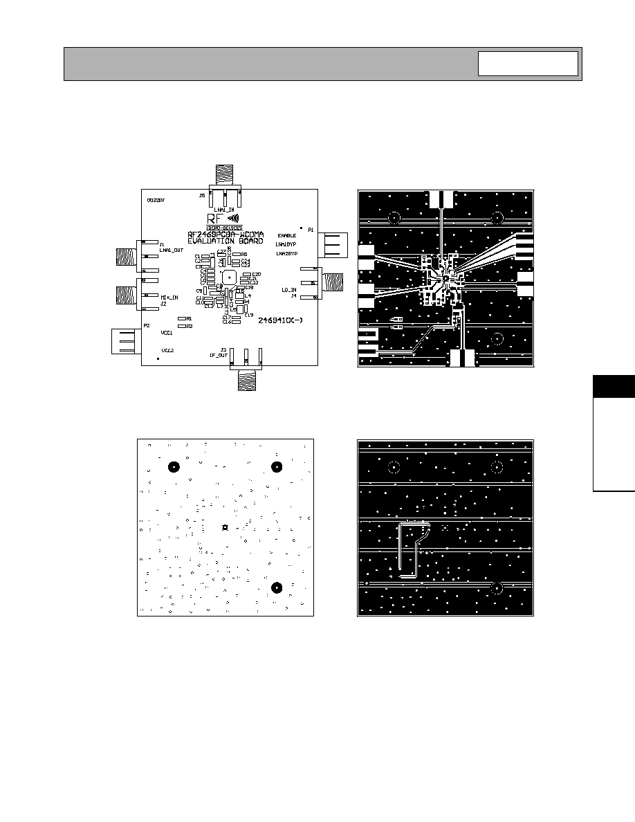
Evaluation Board Layout
Board Size 2.0" x 2.0"
Board Thickness 0.031", Board Material FR-4, Multi-Layer
Assembly
Top
Power Plane
Back
Preliminary
8-44
RF2469
Rev A5 010717
8
F
R
O
N
T
-
E
NDS
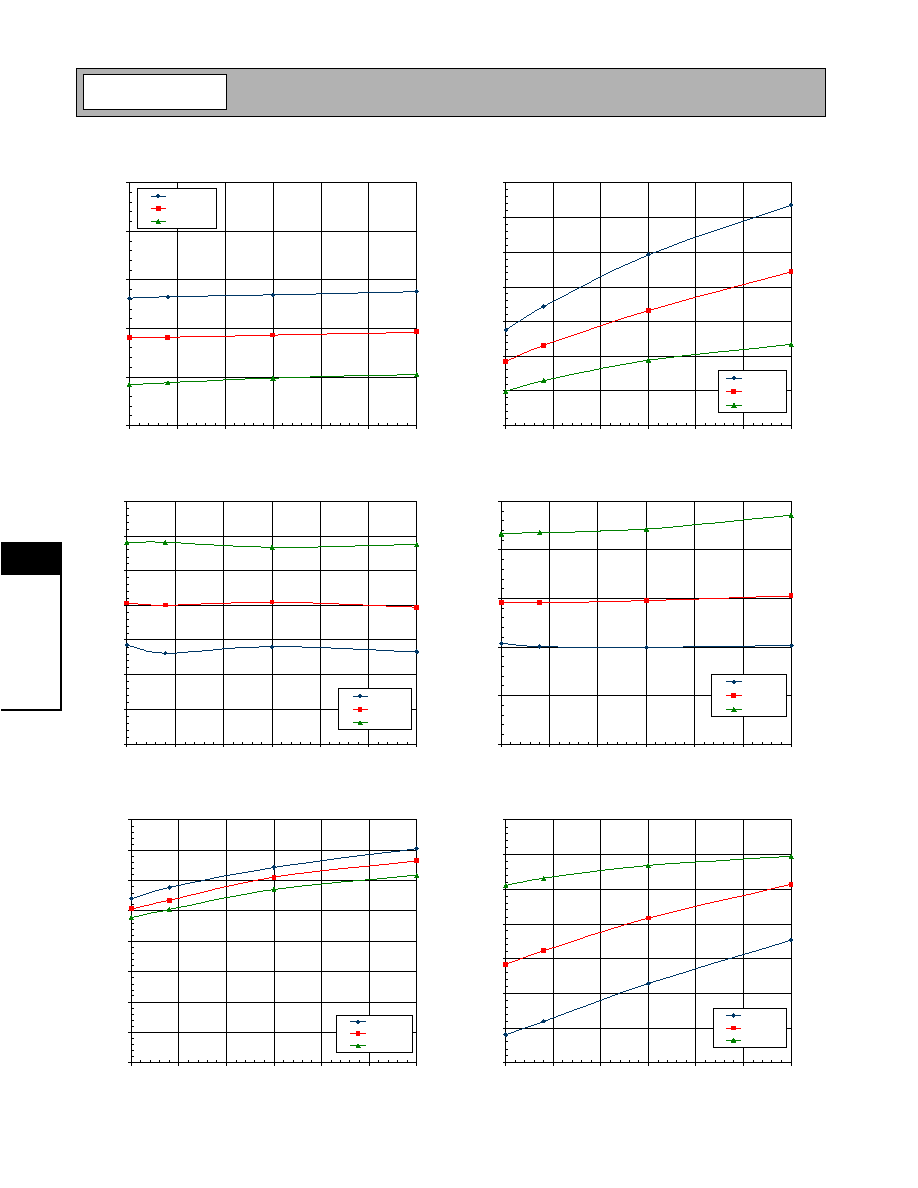
LNA1
(High Gain Mode)
10.2
10.4
10.6
10.8
11.0
11.2
11.4
11.6
2.7
2.8
2.9
3.0
3.1
3.2
3.3
V
CC
(V)
Gain
(dB)
Gain, -30∫
Gain, 25∫
Gain, 85∫
LNA1
(High Gain Mode)
2.0
4.0
6.0
8.0
10.0
12.0
14.0
16.0
2.7
2.8
2.9
3.0
3.1
3.2
3.3
V
CC
(V)
IIP3
(dBm)
IIP3, -30∫
IIP3, 25∫
IIP3, 85∫
LNA1
(High Gain Mode)
0.0
0.5
1.0
1.5
2.0
2.5
2.7
2.8
2.9
3.0
3.1
3.2
3.3
V
CC
(V)
Noise
Figure
(
dB)
NF, -30∫
NF, 25∫
NF, 85∫
LNA1
(Low Gain Mode)
-2.5
-2.0
-1.5
-1.0
-0.5
0.0
2.7
2.8
2.9
3.0
3.1
3.2
3.3
V
CC
(V)
Gain
(dB)
Gain, -30∫
Gain, 25∫
Gain, 85∫
LNA1
(Low Gain Mode)
15.0
17.0
19.0
21.0
23.0
25.0
27.0
29.0
31.0
2.7
2.8
2.9
3.0
3.1
3.2
3.3
V
CC
(V)
IIP3
(dBm)
IIP3, -30∫
IIP3, 25∫
IIP3, 85∫
LNA1
(Low Gain Mode)
0.0
0.5
1.0
1.5
2.0
2.5
3.0
3.5
2.7
2.8
2.9
3.0
3.1
3.2
3.3
V
CC
(V)
Noise
Figure
(
dB)
NF, -30∫
NF, 25∫
NF, 85∫
Preliminary
8-45
RF2469
Rev A5 010717
8
F
R
O
N
T
-
E
NDS
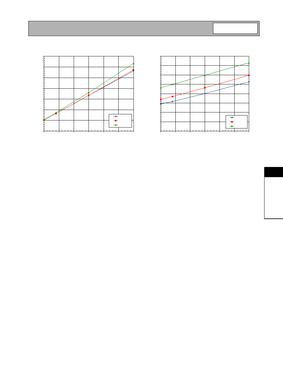
Total Current
(LNA1BYP=LNA2BYP=EN=0)
6.0
6.5
7.0
7.5
8.0
8.5
9.0
9.5
2.7
2.8
2.9
3.0
3.1
3.2
3.3
V
CC
(V)
I
CC
(mA)
Icc, -30∫
Icc, 25∫
Icc, 85∫
Total Current
(LNA1BYP=LNA2BYP=EN=1)
0.0
5.0
10.0
15.0
20.0
25.0
30.0
35.0
40.0
2.7
2.8
2.9
3.0
3.1
3.2
3.3
V
CC
(V)
I
CC
(mA)
Icc, -30∫
Icc, 25∫
Icc, 85∫
Preliminary
8-46
RF2469
Rev A5 010717
8
F
R
O
N
T
-
E
NDS
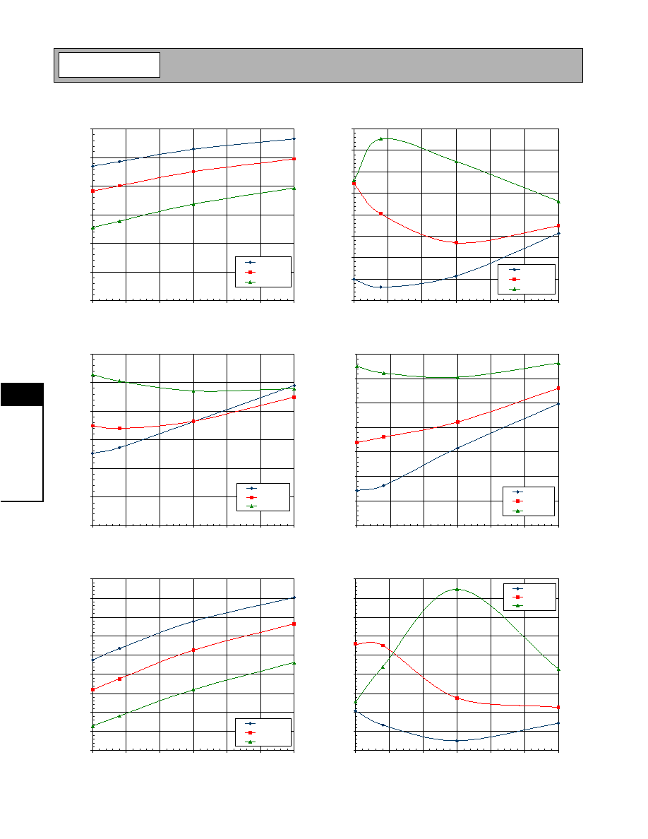
Mixer/LNA2, Low Gain Mode (LNA2BYP=0),
LO @ -10dBm
0.0
2.0
4.0
6.0
8.0
10.0
12.0
2.7
2.8
2.9
3.0
3.1
3.2
3.3
V
CC
(V)
Gain
(dB)
Gain, -30∫
Gain, 25∫
Gain, 85∫
Mixer/LNA2, Low Gain Mode (LNA2BYP=0),
LO @ -10dBm
0.0
1.0
2.0
3.0
4.0
5.0
6.0
7.0
8.0
2.7
2.8
2.9
3.0
3.1
3.2
3.3
V
CC
(V)
IIP3
(dBm)
IIP3, -30∫
IIP3, 25∫
IIP3, 85∫
Mixer/LNA2, Low Gain Mode (LNA2BYP=0),
LO @ -10dBm
15.0
17.0
19.0
21.0
23.0
25.0
27.0
2.7
2.8
2.9
3.0
3.1
3.2
3.3
V
CC
(V)
IIP2
(dBm)
IIP2, -30∫
IIP2, 25∫
IIP2, 85∫
Mixer/LNA2 IF, Low Gain Mode (LNA2BYP=0),
LO @ -10dBm
8.0
8.5
9.0
9.5
10.0
10.5
11.0
11.5
2.7
2.8
2.9
3.0
3.1
3.2
3.3
V
CC
(V)
Noise
Figure
(
dB)
NF, -30∫
NF, 25∫
NF, 85∫
Mixer/LNA2, High Gain Mode (LNA2BYP=1),
LO @ -10dBm
15.0
16.0
17.0
18.0
19.0
20.0
21.0
22.0
23.0
24.0
2.7
2.8
2.9
3.0
3.1
3.2
3.3
V
CC
(V)
Gain
(dB)
Gain, -30∫
Gain, 25∫
Gain, 85∫
Mixer/LNA2, High Gain Mode (LNA2BYP=1),
LO @ -10dBm
-9.0
-8.0
-7.0
-6.0
-5.0
-4.0
-3.0
-2.0
-1.0
0.0
2.7
2.8
2.9
3.0
3.1
3.2
3.3
V
CC
(V)
IIP3
(dBm)
IIP3, -30∫
IIP3, 25∫
IIP3, 85∫
Preliminary
8-47
RF2469
Rev A5 010717
8
F
R
O
N
T
-
E
NDS
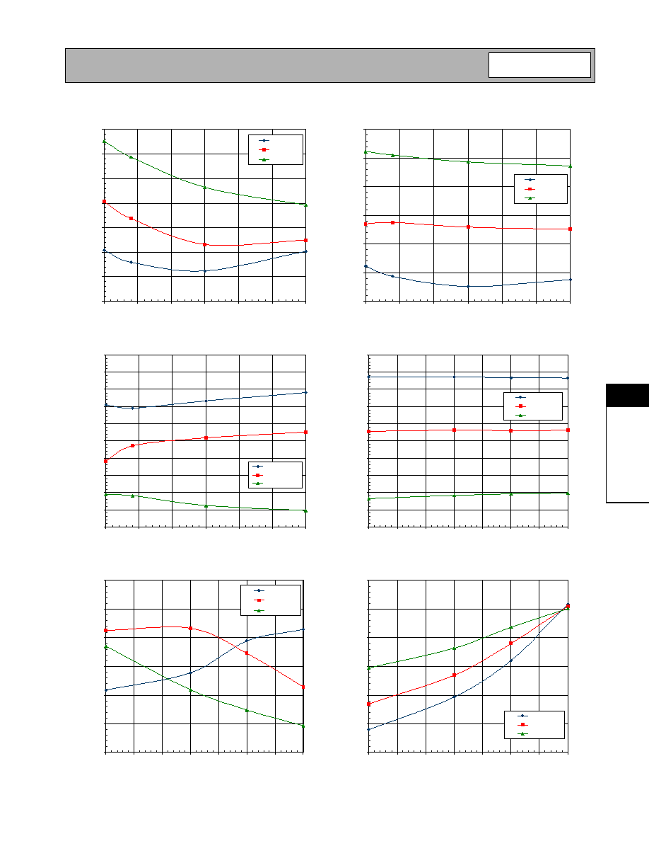
Mixer/LNA2, High Gain Mode (LNA2BYP=1),
LO @ -10dBm
10.0
11.0
12.0
13.0
14.0
15.0
16.0
17.0
2.7
2.8
2.9
3.0
3.1
3.2
3.3
V
CC
(V)
IIP2
(dBm)
IIP2, -30∫
IIP2, 25∫
IIP2, 85∫
Mixer/LNA2, High Gain Mode (LNA2BYP=1),
LO @ -10dBm
3.0
3.5
4.0
4.5
5.0
5.5
6.0
2.7
2.8
2.9
3.0
3.1
3.2
3.3
V
CC
(V)
Noise
Figure
(
dB)
NF, -30∫
NF, 25∫
NF, 85∫
Mixer/LNA2 LO to IF Leakage
(LNA2BYP=1)
-45.0
-43.0
-41.0
-39.0
-37.0
-35.0
-33.0
-31.0
-29.0
-27.0
-25.0
2.7
2.8
2.9
3.0
3.1
3.2
3.3
V
CC
(V)
LO
to
IF
Leakage
(dB)
Isolation, -30∫
Isolation, 25∫
Isolation, 85∫
Mixer/LNA2, High Gain Mode (LNA2BYP=1),
V
CC
@ 2.78V
16.0
16.5
17.0
17.5
18.0
18.5
19.0
19.5
20.0
20.5
21.0
-10.0
-9.0
-8.0
-7.0
-6.0
-5.0
-4.0
-3.0
LO (dBm)
Gain
(dB)
Gain, -30∫
Gain, 25∫
Gain, 85∫
Mixer/LNA2 IF, High Gain Mode (LNA2BYP=1),
V
CC
=2.78V
-12.0
-10.0
-8.0
-6.0
-4.0
-2.0
0.0
-10.0
-9.0
-8.0
-7.0
-6.0
-5.0
-4.0
-3.0
LO (dBm)
IIP3
(dBm)
IIP3, -30∫
IIP3, 25∫
IIP3, 85∫
Mixer/LNA2 IF, High Gain Mode (LNA2BYP=1),
V
CC
=2.78V
10.0
12.0
14.0
16.0
18.0
20.0
22.0
-10.0
-9.0
-8.0
-7.0
-6.0
-5.0
-4.0
-3.0
LO (dBm)
IIP2
(dBm)
IIP2, -30∫
IIP2, 25∫
IIP2, 85∫

Preliminary
8-48
RF2469
Rev A5 010717
8
F
R
O
N
T
-
E
NDS
Low Current Configuration
External resistors can set different bias currents for LNA1 (pin 3), LNA2 (pin 4, also called the preamplifier of the mixer),
and mixer (pin 17). Customers have the flexibility to choose the most suitable bias current, and therefore the perfor-
mance, of the IC. The charts on the following page reflect different bias currents for the RF2469.
The currents were calculated using the following equations.
LNA1 current (R1)= Total Current (LNA1= EN =1, LNA2 =0)-Total Current (EN= 1, LNA1= LNA2=0)+1.6
1.6 is the bypass current of LNA1
Mixer/LNA2 current (R2)=Total Current (LNA1= 0, LNA2 =EN =1)-Total Current (LNA1 =LNA2= 0, EN= 1)+1.4+ 10.2
1.4 is the bypass current of LNA2; 10.2 is the mixer (LO buffer included)
Mixer Only current (R5)=Total Current (EN =LNA2= 1, LNA1= 0)-4.5
4.5 is the bypass current of the LNA1 (1.6mA)+ LNA2 high mode current (2.9mA)
RFMD chose a low current configuration of the RF2469, by using R1= 3k
, R2=3.6k
, and R5=1k
in the evaluation
board, and the following lab results over temperature were obtained.
LNA1 High Mode
Temp
(∞C)
Frequency
(MHz)
P
IN
(dBm)
V
CC
(V
DC
)
Gain
(dB)
IIP3
(dBm)
Noise Figure
(dB)
Total
Current
-30
2140
-25
2.78
+7.97
-3.78
+1.72
+11.33
+25
2140
-25
2.78
+8.81
+2.32
+1.95
+12.36
+85
2140
-25
2.78
+9.70
+7.71
+2.37
+16.45
Total Current (mA) is when LNA1BYP=LNA2BYP2=EN =1.
Mixer/LNA2 BYP High Mode
Temp
(∞C)
Frequency
(MHz)
P
IN
(dBm)
LO Frequency
(MHz)
P
IN
LO
(dBm)
V
CC
(V
DC
)
Gain
(dB)
IIP3
(dBm)
Noise Figure
(dB)
-30
2140
-25
2330
-10
2.78
+18.73
-8.16
+3.98
+25
2140
-25
2330
-10
2.78
+17.74
+5.13
+4.54
+85
2140
-25
2330
-10
2.78
+16.67
-3.66
+5.19

Preliminary
8-49
RF2469
Rev A5 010717
8
F
R
O
N
T
-
E
NDS
LNA Gain, Noise Figure and IIP3 versus I
CC
- LNA1 Only
(LNA High Gain)
0.0
2.0
4.0
6.0
8.0
10.0
12.0
1.0
2.0
3.0
4.0
5.0
6.0
7.0
8.0
9.0
10.0
I
CC
(mA)
Gain
and
Noise
Figure
(
dB)
-2.0
0.0
2.0
4.0
6.0
8.0
10.0
12.0
14.0
16.0
IIP3
(dBm)
Gain (dB)
NF (dB)
IIP3 (dBm)
Resistor (R1) versus I
CC
(mA) - LNA Only
(LNA High Gain)
0.0
1.0
2.0
3.0
4.0
1.0
3.0
5.0
7.0
9.0
11.0
I
CC
(mA)
Resistor
R1
(k
)
Mixer Gain, Noise Figure and IIP3 versus I
CC
-
Mixer/LNA2 BYP High (LO=2330MHz @ -10dBm, sweeping R2)
0.0
2.0
4.0
6.0
8.0
10.0
12.0
14.0
16.0
18.0
20.0
11.0
11.5
12.0
12.5
13.0
13.5
I
CC
(mA)
Gain
and
Noise
Figure
(
dB)
-6.0
-4.0
-2.0
0.0
IIP3
(dBm)
Gain (dB)
NF (dB)
IIP3 (dBm)
Resistor (R2) versus I
CC
- Mixer/LNA2 BYP High
(LO=2330MHz @ -10dBm)
1.5
2.0
2.5
3.0
3.5
4.0
4.5
5.0
11.0
11.5
12.0
12.5
13.0
13.5
I
CC
(mA)
Resistor
R2
(k
)
Mixer Gain, Noise Figure and IIP3 versus I
CC
-
Mixer/LNA2 BYP High (LO=2330MHZ @ 019dBm, sweeping R5)
0.0
5.0
10.0
15.0
20.0
25.0
7.0
8.0
9.0
10.0
11.0
12.0
13.0
14.0
I
CC
(mA)
Gain
and
Noise
Figure
(
dB)
-10.0
-9.0
-8.0
-7.0
-6.0
-5.0
-4.0
-3.0
-2.0
-1.0
0.0
IIP3
(dBm)
Gain (dB)
NF (dB)
IIP3 (dBm)
Resistor (R5) versus I
CC
- Mixer/LNA2 BYP High
(LO=2330MHz @ -10dBm)
0.4
0.6
0.8
1.0
1.2
1.4
1.6
6.0
7.0
8.0
9.0
10.0
11.0
12.0
13.0
14.0
I
CC
(mA)
Resistor
R5
(k
)

Preliminary
8-50
RF2469
Rev A5 010717
8
F
R
O
N
T
-
E
NDS