
4-507
Product Description
Ordering Information
Typical Applications
Features
Functional Block Diagram
RF Micro Devices, Inc.
7628 Thorndike Road
Greensboro, NC 27409, USA
Tel (336) 664 1233
Fax (336) 664 0454
http://www.rfmd.com
Optimum Technology MatchingÆ Applied
Si BJT
GaAs MESFET
GaAs HBT
Si Bi-CMOS
SiGe HBT
Si CMOS
InGaP/HBT
GaN HEMT
SiGe Bi-CMOS
1
2
3
5
4
RF OUT
PD
VCC
GND
RF IN
RF2472
2.4GHz LOW NOISE AMPLIFIER WITH ENABLE
∑ TDMA/CDMA PCS LNA
∑ TDMA/CDMA/FM Cellular LNA
∑ ISM Band LNA/Driver
∑ Low Noise Transmit Driver Amplifier
∑ General Purpose Amplification
∑ Commercial and Consumer Systems
The RF2472 is a general purpose, low-cost, high-perfor-
mance amplifier designed for operation from a 2.7V to 4V
supply with low current consumption. The device is opti-
mized for 2.4GHz LNA applications, but is also useful for
1.9GHz PCS and K-PCS, 900MHz ISM, and 1.5GHz
GPS applications. The RF2472 is available in a very
small industry-standard SOT23 5-lead surface mount
package, enabling compact designs which conserve
board space.
∑ DC to >6GHz Operation
∑ 2.7V to 4.0V Single Supply
∑ High Input IP
3
∑ 1.5dB Noise Figure at 2400MHz
∑ 14dB Gain at 2400MHz
∑ Low Current Consumption of 6mA at 3V
RF2472
2.4GHz Low Noise Amplifier with Enable
RF2472 PCBA-410Fully Assembled Evaluation Board, 2.4GHz
RF2472 PCBA-411Fully Assembled Evaluation Board, 1.9GHz
0
Rev A8 030124
1
1.60
+ 0.01
0.400
2.80
+ 0.20
2.90
+ 0.10
0.45
+ 0.10
3∞ MAX
0∞ MIN
0.127
0.15
0.05
1.44
1.04
Dimensions in mm.
0.950
Package Style: SOT 5 Lead
Preliminary
!

Preliminary
4-508
RF2472
Rev A8 030124
Absolute Maximum Ratings
Parameter
Rating
Unit
Supply Voltage
-0.5 to 4.0
V
Input RF Level
0
dBm
Operating Ambient Temperature
-40 to +85
∞C
Storage Temperature
-40 to +150
∞C
Parameter
Specification
Unit
Condition
Min.
Typ.
Max.
Overall
T=27∞C, V
CC
=3.0V
Frequency Range
DC to >6000
MHz
2.4GHz LNA Operation
T=27∞C, V
CC
=3.0V, Freq=2440MHz
Gain
13.0
14.6
17.0
dB
Noise Figure
1.5
dB
Input IP3
+8.0
+10.0
+20.0
dBm
Two tones at 1MHz spacing, -15dBm output
Input P
1dB
-10
dBm
PCS and K-PCS LNA
Operation
T=27∞C, V
CC
=3.0V, Freq=1960MHz
Gain
16.3
dB
Noise Figure
1.4
dB
Input IP3
+8
dBm
Two tones at 1MHz spacing, -12dBm output
Input P
1dB
-12
dBm
Power Supply
Operating Voltage
2.7 to 3.6
V
Operating Current
4.0
6.0
8.0
mA
V
CC
=3.0V, PD=3.0V
<1.0
3.0
µ
A
V
CC
=3.0V, PD=0V
Caution! ESD sensitive device.
RF Micro Devices believes the furnished information is correct and accurate
at the time of this printing. However, RF Micro Devices reserves the right to
make changes to its products without notice. RF Micro Devices does not
assume responsibility for the use of the described product(s).

Preliminary
4-509
RF2472
Rev A8 030124
Pin
Function
Description
Interface Schematic
1
VCC
Supply connection. An external bypass capacitor may be required in
some applications.
See pin 3.
2
GND
Ground connection. Keep traces physically short and connect immedi-
ately to ground plane for best performance.
3
RF IN
RF input pin. This pin is DC coupled and matched to 50
at 2.4GHz.
4
PD
Power down pin.This pin enables the bias to the amplifier. To turn the
amplifier on, this pin should be connected to V
CC
. Connecting this pin
to ground, will turn the amplifier off and reduce the current draw to
below 1
µ
A. This pin is a CMOS input. There is no DC current draw
other than the transient current required to charge or discharge the
gate capacitance (less than 5pF).
5
RF OUT
LNA Output pin.This pin is an open-collector output. It must be biased
to V
CC
through a choke or matching inductor. This pin is typically
matched to 50
with a shunt bias/matching inductor and series block-
ing/matching capacitor. Refer to application schematics.
See pin 3.
RF IN
RF OUT
VCC
BIAS
PD

Preliminary
4-510
RF2472
Rev A8 030124
Theory of Operation
The RF2472 is a low-noise amplifier with internal bias
circuitry. It is DC-coupled on the input and output;
therefore, it can be used to arbitrarily low frequency. It
has useful gain to above 6GHz. Its design is optimized
for use at 2.4GHz. Because of the high-frequency
gain, the designer must take care to ensure that the
device will remain stable outside the desired operating
frequency. The RF2472 is capable of providing out-
standing linearity, but to achieve this high performance,
the circuit designer must pay attention to the termina-
tions that are presented to low-frequency intermodula-
tion products.
Stability
The RF2472 must be stabilized for frequencies outside
of the desired operating range. Ground connections
should be kept as short as possible. Wherever practi-
cal, ground should be provided by a via hole directly to
a continuous ground layer. Highly reflective termina-
tions to the RF input and output pins should be avoided
whenever possible. In most circumstances, a resistor
in parallel with an inductor in the bias line on pin 5 will
improve the stability of the circuit. See the application
schematics for examples. The 10nH inductor in the
bias line is part of an output impedance matching cir-
cuit. At higher frequencies, the impedance of the
matching circuit, alone, would become highly inductive.
The large reactive termination of the output port could
cause the circuit to oscillate at a high frequency. The
resistance in parallel with the inductor adds a real part
to the high-frequency termination that will have a stabi-
lizing effect on the circuit.
Linearity
The 22nF bypass and coupling capacitors in the appli-
cation schematics may seem excessively large for cir-
cuits intended to operate at 1.9GHz and 2.4GHz.
These large capacitors provide a low impedance path
to ground for second-order mixing products that leads
to improved third-order intermodulation performance.
The effect is most easily seen for the input coupling
capacitor. A 100pF capacitor would provide low
enough impedance to couple a 2.4GHz signal into the
input pin of the RF2472. However, low-frequency inter-
modulation products caused by second-order nonlin-
earities would be presented with a large reactive
impedance at the input pin. Relatively large voltages
for these low-frequency products would be allowed to
mix with the fundamental signals at the input pin,
resulting in relatively large, in-band, third-order prod-
ucts.
With a large coupling capacitor, the low-frequency
products would be presented with a low impedance,
via the input source impedance, resulting in a lower
voltage at the input pin. These products, in turn, would
mix at a lower level with the fundamental signals to
produce lower in-band, third-order products.
Some designers may be concerned about the self-res-
onant frequency of large coupling capacitors. A 22nF
capacitor will probably pass through self resonance
below 100MHz. Beyond resonance, the reactance of
the capacitor will turn inductive, but the internal losses
of the capacitor will usually prevent the component
from exhibiting a large reactive impedance.
Third-Order Intercept versus 1-dB Compression
Point
For many devices, the third-order intercept point is
approximately 10dB higher than the 1-dB compression
point. This rule of thumb does not apply for the
RF2472. It is normal to find that the third-order inter-
cept point is 20 dB higher than the 1-dB compression
point. This behavior is common for SiGe devices. The
reason for the difference is that the 10dB rule is based
on a simple third-order polynomial model for device
nonlinearities. For SiGe devices this simple model is
not a good fit.

Preliminary
4-511
RF2472
Rev A8 030124
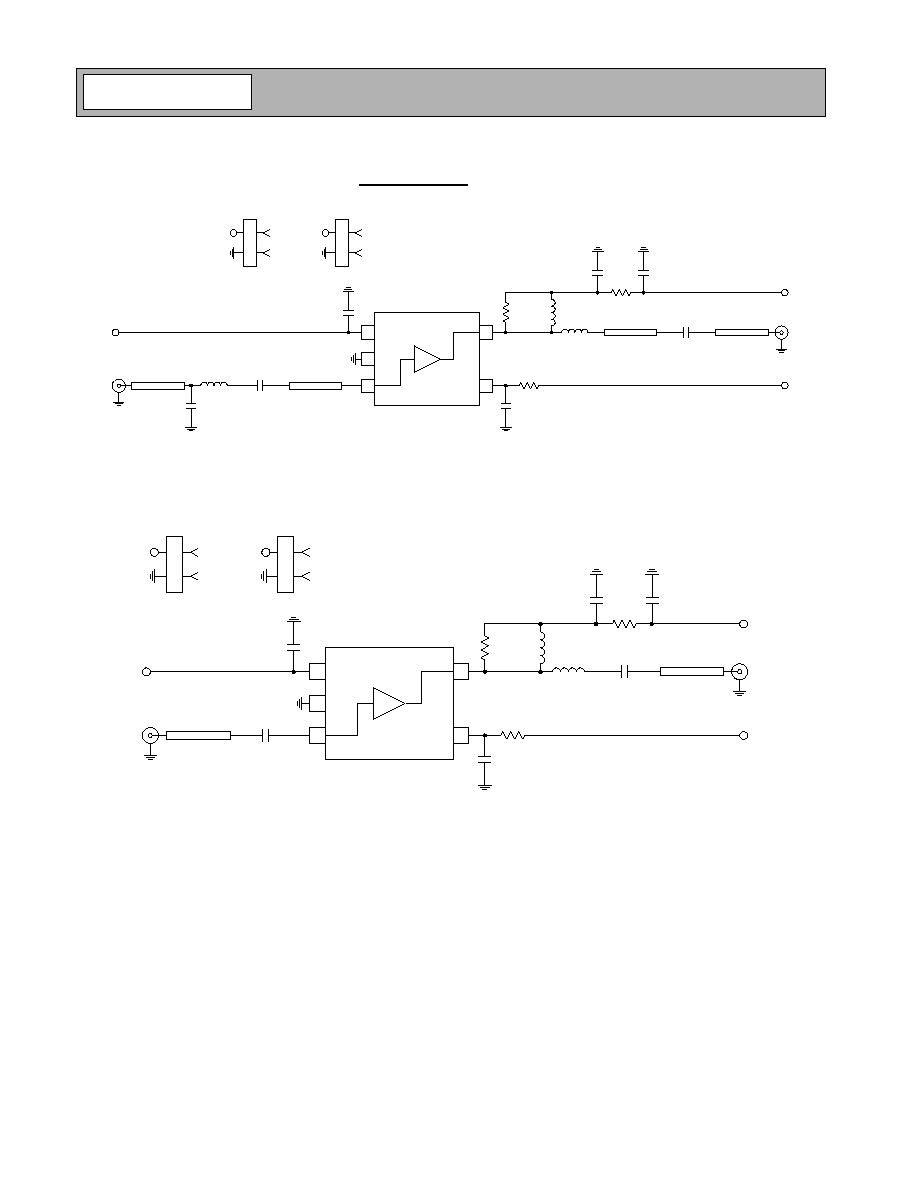
Application Schematic - 1.9GHz
Application Schematic - 2.4GHz
1
2
3
5
4
RF IN
RF OUT
V
CC
PD
5.6 nH
2.7 nH
22 nF
22 nF
0.5 pF
22 nF
1.8 k
10 nH
V
CC
22 nF
22 pF
1
2
3
5
4
RF IN
V
CC
22 nF
22 nF
PD
RF OUT
5.6 nH
22 nF
1.0 k
10 nH
V
CC
22 pF
22 nF
Preliminary
4-512
RF2472
Rev A8 030124
Evaluation Board Schematic - 1.9GHz
(Download Bill of Materials from www.rfmd.com.)
Evaluation Board Schematic - 2.4GHz
1
2
3
5
4
J2
RF OUT
J1
RF IN
PD
C8
15 nF
C2
15 nF
VCC
C1
10 nF
L1
10 nH
R3
10
C7
15 nF
C6
3 pF
VCC
C4
15 nF
R1
1 k
U1
50
µ
strip
R4
1.8 k
L2
5.6 nH
50
µ
strip
50
µ
strip
L3
2.7 nH
C3
0.5 pF
50
µ
strip
GND
P1-1
PD
P1
1
2
GND
P2-1
VCC
1
2
P2
1
2
3
5
4
J2
RF OUT
J1
RF IN
PD
C8
15 nF
P1
1
2
C2
15 nF
VCC
C1
15 nF
L1
10 nH
R3
10
C7
15 nF
C6
3 pF
VCC
C4
15 nF
R1
1 k
U1
50
µ
strip
R4
1.0 k
L2
5.6 nH
50
µ
strip
1
2
P2-1
P2
GND
VCC1
P1-1
PD
GND
2472400-

Preliminary
4-513
RF2472
Rev A8 030124
Evaluation Board Layout - 1.9GHz
Board Size 1.0" x 1.0"
Board Thickness 0.031"; Board Material FR-4
Evaluation Board Layout - 2.4GHz
Board Size 1.0" x 1.0"
Board Thickness 0.031"; Board Material FR-4

Preliminary
4-514
RF2472
Rev A8 030124
0
1.0
1.0
-1.0
10.0
10.0
-1
0.
0
5.0
5.
0
-5
.0
2.0
2
.
0
-
2
.
0
3.0
3.
0
-3
.0
4.0
4.
0
-4
.0
0.2
0.
2
-0
.2
0.4
0
.
4
-
0
.
4
0.6
0
.
6
-
0
.
6
0.8
0
.
8
-
0
.
8
Smith Chart
Swp Max
5.00069GHz
Swp Min
0.1GHz
S1,1
S2,2
Gain versus Frequency
0.0
5.0
10.0
15.0
20.0
25.0
0.0
1.0
2.0
3.0
4.0
5.0
Frequency (GHz)
S21 (dB)