 | –≠–ª–µ–∫—Ç—Ä–æ–Ω–Ω—ã–π –∫–æ–º–ø–æ–Ω–µ–Ω—Ç: RF2480 | –°–∫–∞—á–∞—Ç—å:  PDF PDF  ZIP ZIP |

¸
5-29
5
MO
D
U
LA
T
O
R
S
A
N
D
UP
C
O
N
V
E
R
T
E
RS
Product Description
Ordering Information
Typical Applications
Features
Functional Block Diagram
RF Micro Devices, Inc.
7628 Thorndike Road
Greensboro, NC 27409, USA
Tel (336) 664 1233
Fax (336) 664 0454
http://www.rfmd.com
Optimum Technology MatchingÆ Applied
Si BJT
GaAs MESFET
GaAs HBT
Si Bi-CMOS
SiGe HBT
Si CMOS
1 6
1 5
1 4
1 3
1 2
1 1
1 0
9
1
2
3
4
5
6
7
8
P O W E R
C O N T R O L
-4 5 ∞
+ 4 5 ∞
I R E F
Q R E F
G N D 2
G N D 2
G N D 2
LO
V C C 1
P D
I S IG
Q S IG
G N D 1
G N D 1
G N D 1
V C C 2
G N D 1
R F O U T
RF2480
DIRECT QUADRATURE MODULATOR
∑ Dual-Band CDMA Base Stations
∑ TDMA/TDMA-EDGE Base Stations
∑ GSM-EDGE/EGSM Base Stations
∑ W-CDMA Base Stations
∑ WLAN and WLL Systems
∑ TETRA Systems
The RF2480 is a monolithic integrated quadrature modu-
lator IC capable of universal direct modulation for high-
frequency AM, PM, or compound carriers. This low-cost
IC features excellent linearity, noise floor, and over-tem-
perature carrier suppression performance. The device
implements differential amplifiers for the modulation
inputs, 90∞ carrier phase shift network, carrier limiting
amplifiers, two matched double-balanced mixers, sum-
ming amplifier, and an output RF amplifier which will drive
50
from 800 MHz to 2500MHz. Component matching is
used to obtain excellent amplitude balance and phase
accuracy.
∑ Typical Carrier Suppression>35dBc over
temperature with highly linear operation
∑ Single 5V Power Supply
∑ Integrated RF quadrature network
∑ Digitally controlled Power Down mode
∑ 800MHz to 2500MHz operation
RF2480
Direct Quadrature Modulator
RF2480 PCBA
Fully Assembled Evaluation Board
5
Rev A3 011019
NOTES:
1. Shaded lead is Pin 1.
2. All dimensions are excluding
mold flash.
3. Lead coplanarity - 0.005 with
respect to datum "A".
0.050
0.018
0.014
0.157
0.150
0.393
0.386
0.244
0.229
8∞ MAX
0∞ MIN
0.034
0.016
0.009
0.007
0.068
0.053
0.008
0.004
-A-
Package Style: SOIC-16

5-30
RF2480
Rev A3 011019
5
MO
D
U
LA
T
O
R
S
A
N
D
UP
C
O
N
V
E
R
T
E
RS
Absolute Maximum Ratings
Parameter
Rating
Unit
Supply Voltage
-0.5 to +7.5
V
DC
Input LO and RF Levels
+10
dBm
Operating Ambient Temperature
-40 to +85
∞C
Storage Temperature
-40 to +150
∞C
Parameter
Specification
Unit
Condition
Min.
Typ.
Max.
Carrier Input
T = 25∞C, V
CC
=5V
Frequency Range
800
2500
MHz
Power Level
-6
+6
dBm
Input VSWR
4.5:1
At 900MHz unmatched
2:1
At 1800MHz unmatched
2:1
At 2500MHz unmatched
Modulation Input
Frequency Range
DC
250
MHz
Reference Voltage (V
REF
)
3.0
V
Maximum Modulation (I&Q)
V
REF
± 1.0
V
Gain Asymmetry
0.2
dB
Quadrature Phase Error
3
∞
Input Resistance
30
k
Input Bias Current
40
µ
A
RF Output (~800MHz)
LO= 800MHz, -5dBm; SSB
Maximum Output Power
-3
0
+2
dBm
TETRA I&Q Amplitude= 2V
PP
Over operating temperature.
High-Linearity Output Power
-6
-5
dBm
TETRA I&Q Amplitude= 1.1V
PP
with an
ACPR of -47dBc. Over operating tempera-
ture.
Adjacent Channel
Power Rejection
-47
-52
dBc
TETRA modulation applied with
P
OUT
=-5dBm. Over operating temperature.
Output P1dB
+2
+3
dBm
Over operating temperature.
IM3 Suppression
-39
-40
dBc
2kHz offset (9kHz, 11kHz) at -6dBm/tone.
Over operating temperature.
IM5 Suppression
-49
-59
dBc
2kHz offset (9kHz, 11kHz) at -6dBm/tone.
Over operating temperature.
IM7 Suppression
-49
-71
dBc
2kHz offset (9kHz, 11kHz) at -6dBm/tone.
Over operating temperature.
Carrier Suppression
-25
-30
dBc
Unadjusted performance.
Sideband Suppression
-25
-30
dBc
Unadjusted performance.
Broadband Noise Floor
-150
-145
dBm/Hz
26MHz offset with TETRA signal applied
P
OUT
=-5dBm.
Caution! ESD sensitive device.
RF Micro Devices believes the furnished information is correct and accurate
at the time of this printing. However, RF Micro Devices reserves the right to
make changes to its products without notice. RF Micro Devices does not
assume responsibility for the use of the described product(s).

5-31
RF2480
Rev A3 011019
5
MO
D
U
LA
T
O
R
S
A
N
D
UP
C
O
N
V
E
R
T
E
RS
Parameter
Specification
Unit
Condition
Min.
Typ.
Max.
RF Output (~900MHz)
LO= 880MHz, -5dBm; SSB
Maximum Output Power
0
+4
dBm
I&Q Amplitude= 2V
PP
High-Linearity Output Power
-11
dBm
I&Q Amplitude= 0.325V
PP
Carrier Suppression
50
dB
T= 25∞C; P
OUT
= -11dBm (meets CDMA base
station requirements); optimized I,Q DC off-
sets
35
dB
Over Temperature (Temperature cycled from
-40∞C to +85∞C after optimization at
T= 25∞C; P
OUT
= -11dBm)
Sideband Suppression
50
dB
T= 25∞C; P
OUT
= -11dBm; optimized I,Q DC
offsets
35
dB
Over Temperature (Temperature cycled from
-40∞C to +85∞C after optimization at
T= 25∞C; P
OUT
= -11dBm)
Output Impedance
13-j:25
Broadband Noise Floor
-153.0
dBm/Hz
At 20MHz offset, V
CC
=5V; Tied to V
REF
:
ISIG, QSIG, IREF, and QREF.
RF Output (~2000 MHz)
LO= 2000MHz, -5dBm; SSB
Maximum Output Power
-7
-3
dBm
I&Q Amplitude= 2V
PP
High-Linearity Output Power
-17
dBm
I&Q Amplitude= 0.325V
PP
Carrier Suppression
50
dB
T= 25∞C; P
OUT
= -17dBm; optimized I,Q DC
offsets
35
dB
Temperature cycled from -40∞C to +85∞C
after optimization at T = 25∞C; P
OUT
=-17dBm
Sideband Suppression
50
dB
T= 25∞C; P
OUT
= -17dBm; optimized I,Q DC
offsets
40
dB
Temperature cycled from -40∞C to +85∞C
after optimization at T = 25∞C; P
OUT
=-17dBm
Output Impedance
58-j11
Broadband Noise Floor
-158.0
dBm/Hz
At 20MHz offset, V
CC
=5V; Tied to V
REF
:
ISIG, QSIG, IREF, and QREF.
Power Down
Turn On/Off Time
100
ns
PD Input Resistance
50
k
Power Control "ON"
2.8
V
Threshold voltage
Power Control "OFF"
1.0
1.2
V
Threshold voltage
Power Supply
Voltage
5
V
Specifications
4.5
6.0
V
Operating Limits
Current
50
mA
Operating
25
µ
A
Power Down
5-32
RF2480
Rev A3 011019
5
MO
D
U
LA
T
O
R
S
A
N
D
UP
C
O
N
V
E
R
T
E
RS
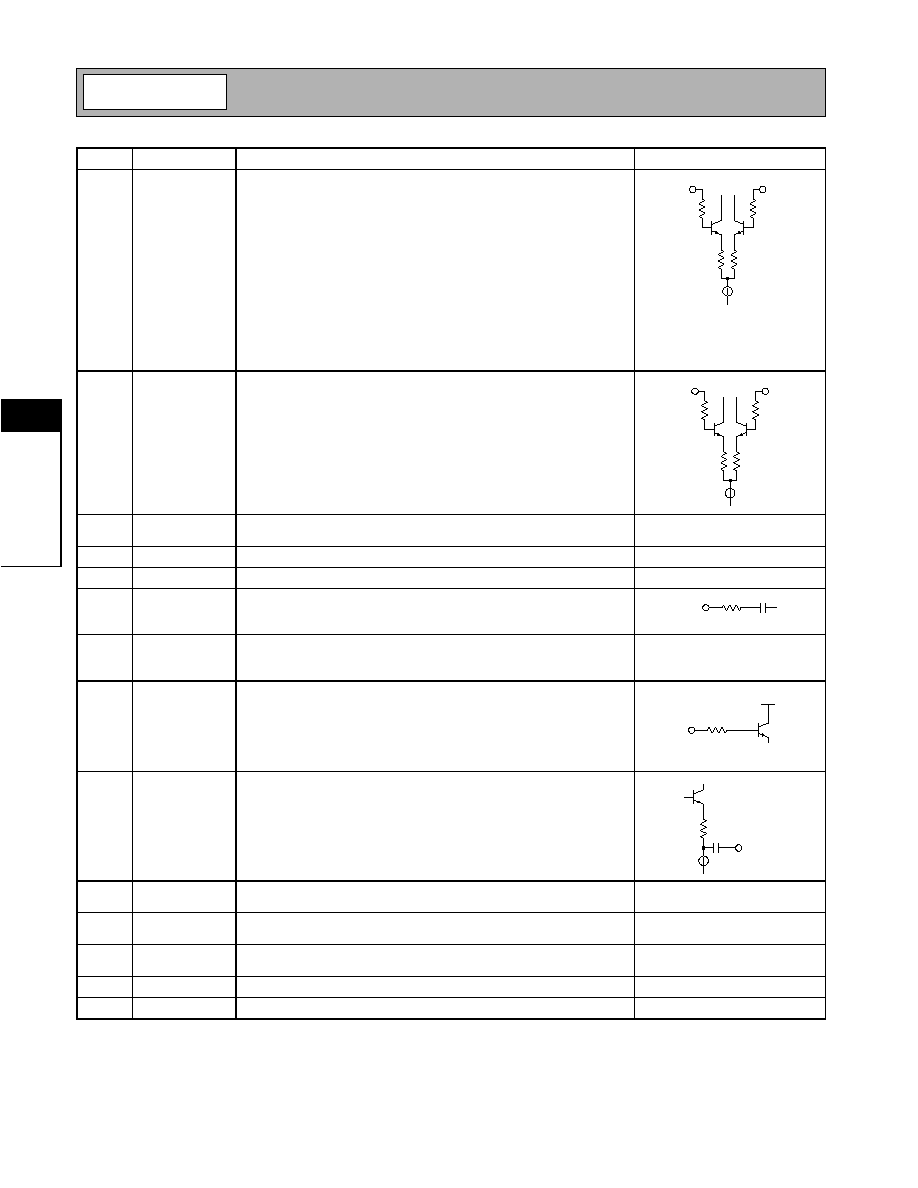
Pin
Function
Description
Interface Schematic
1
I REF
Reference voltage for the I mixer. This voltage should be the same as
the DC voltage supplied to the I SIG pin. A voltage of 3.0V is recom-
mended. The SIG and REF inputs are inputs of a differential amplifier.
Therefore the REF and SIG inputs are interchangeable. If swapping the
I SIG and I REF pins, the Q SIG and Q REF also need to be swapped
to maintain the correct phase. It is also possible to drive the SIG and
REF inputs in a balanced mode. This will increase the gain.
For optimum carrier suppression, the DC voltages on I REF, Q REF, I
SIG and Q SIG should be adjusted slightly to compensate for inherent
undesired internal DC offsets; for optimum sideband suppression,
phase and signal amplitude on IREF, Q REF, I SIG and Q SIG should
be adjusted slightly to compensate for inherent undesired internal off-
sets. See RFMD AN0001 for more detail.
2
Q REF
Reference voltage for the Q mixer. This voltage should be the same as
the DC voltage supplied to the Q SIG pin. A voltage of 3.0V is recom-
mended. See pin 1 for more details.
3
GND2
Ground connection of the LO phase shift network. This pin should be
connected directly to the ground plane.
4
GND2
Same as pin 3.
5
GND2
Same as pin 3.
6
LO
The input of the phase shifting network. This pin has an internal DC
blocking capacitor. This port is voltage driven so matching at different
frequencies is not required.
7
VCC1
Power supply for all circuits except the RF output stage. An external
capacitor is needed if no other low frequency bypass capacitor is
nearby.
8
PD
Power Down control. When this pin is "low", all circuits are shut off. A
"low" is typically 1.2V or less at room temperature.When this pin is
"high" (V
CC
), all circuits are operating normally. If PD is below V
CC
, out-
put power and performance will be degraded. Operating in this region
is not recommended, although it might be useful in some applications
where power control is required.
9
RF OUT
RF Output. This pin has an internal DC blocking capacitor. At some fre-
quencies, external matching may be needed to optimize output power.
10
GND3
Ground connection for the RF output stage. This pin should be con-
nected directly to the ground plane.
11
VCC2
Power supply for the RF output amplifier. An external capacitor is
needed if no other low frequency bypass capacitor is near by.
12
GND1
Ground connection for the LO and baseband amplifiers, and for the
mixers. This pin should be connected directly to the ground plane.
13
GND1
Same as pin 12.
14
GND1
Same as pin 12.
425
425
100
100
I REF
I SIG
425
425
100
100
Q REF
Q SIG
LO
200
PD
V
CC
RF OUT

5-33
RF2480
Rev A3 011019
5
MO
D
U
LA
T
O
R
S
A
N
D
UP
C
O
N
V
E
R
T
E
RS
Application Schematic
DC-Coupled
Pin
Function
Description
Interface Schematic
15
Q SIG
Baseband input to the Q mixer. This pin is DC-coupled. Maximum out-
put power is obtained when the input signal has a peak to peak ampli-
tude of 2V; for highly linear operation, the input signal (and output
power) must be reduced appropriately. The recommended DC level for
this pin is 3.0V. The peak minimum voltage on this pin (V
REF
- peak
modulation amplitude) should never drop below 2.0V. The peak maxi-
mum voltage on this pin (V
REF
+ peak modulation amplitude) should
never exceed 4.0V. See pin 1 for more details.
16
I SIG
Baseband input to the I mixer. This pin is DC-coupled. Maximum output
power is obtained when the input signal has a peak to peak amplitude
of 2V; for highly linear operation, the input signal (and output power)
must be reduced appropriately. The recommended DC level for this pin
is 3.0V. The peak minimum voltage on this pin (V
REF
- peak modulation
amplitude) should never drop below 2.0V. The peak maximum voltage
on this pin (V
REF
+ peak modulation amplitude) should never exceed
4.0V. See pin 1 for more details.
425
425
100
100
Q REF
Q SIG
425
425
100
100
I REF
I SIG
1
2
3
4
5
6
7
8
16
15
14
13
12
11
10
9
P O W E R
C O N T R O L
-4 5∞
+ 4 5 ∞
1 00 n F
V
C C
1 00 n F
1 00 n F
P D
LO IN
I
R E F
I S IG
Q S IG
V
C C
10 0 nF
R F O U T
1 00 n F
Q
R E F

5-34
RF2480
Rev A3 011019
5
MO
D
U
LA
T
O
R
S
A
N
D
UP
C
O
N
V
E
R
T
E
RS
Evaluation Board Schematic
(Download Bill of Materials from www.rfmd.com.)
1
2
3
4
5
6
7
8
16
15
14
13
12
11
10
9
POWER
CONTROL
C1
100 nF
P1-1
C3
100 nF
P1-1
P2-1
C2
100 nF
LO IN
J1
RF OUT
J2
I SIG
J4
Q SIG
J3
2480400-
50
µ
strip
50
µ
strip
50
µ
strip
50
µ
strip
-45∞
+45∞
NC
GND
P1-1
VCC
P1
1
2
3
P2
1
2
3
P2-1
REF
GND
NC

5-35
RF2480
Rev A3 011019
5
MO
D
U
LA
T
O
R
S
A
N
D
UP
C
O
N
V
E
R
T
E
RS
Evaluation Board Layout
Board Size 1.510" x 1.510"
Board Thickness 0.031", FR-4

5-36
RF2480
Rev A3 011019
5
MO
D
U
LA
T
O
R
S
A
N
D
UP
C
O
N
V
E
R
T
E
RS