8-105
8
F
R
O
N
T
-
E
NDS
Product Description
Ordering Information
Typical Applications
Features
Functional Block Diagram
RF Micro Devices, Inc.
7628 Thorndike Road
Greensboro, NC 27409, USA
Tel (336) 664 1233
Fax (336) 664 0454
http://www.rfmd.com
Optimum Technology MatchingÆ Applied
Si BJT
GaAs MESFET
GaAs HBT
Si Bi-CMOS
¸
SiGe HBT
Si CMOS
1
2
3
4
5
6
7
8
9
10
11
12
24
23
22
21
20
19
18
17
16
15
14
13
NC
VCC1
VCC2
GND1
LNA IN
GND2
GND3
NC
GND4
VCC3
LO BUFF EN
LO IN
NC
GND9
VCC4
GND8
LNA OUT
GND7
MIX RF IN
GND6
IF-
IF+
GND5
LO BUFF OUT
RF2486
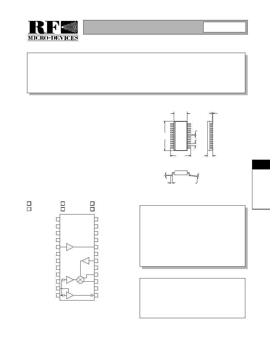
PCS LOW NOISE AMPLIFIER/MIXER
∑ CDMA/TDMA/DCS1900 PCS Systems
∑ PHS 1500/WLAN 2400 Systems
∑ General Purpose Downconverter
∑ Micro-Cell PCS Base Stations
∑ Portable Battery-Powered Equipment
The RF2486 is a monolithic integrated receiver front-end
for PCS, PHS, and WLAN applications. The IC contains
all of the required components to implement the RF func-
tions of the receiver front-end except for the passive filter-
ing and LO generation. It contains an LNA (low-noise
amplifiers), a double-balanced Gilbert cell mixer, a bal-
anced IF output, an LO isolation buffer amplifier, and an
LO output buffer amplifier for providing the buffered LO
signal as an output. The IC is designed to operate from a
single 3.6V power supply.
∑ Complete Receiver Front-End
∑ High Dynamic Range
∑ Single 3.6V Power Supply
∑ External LNA IP3 Adjustment
∑ 1500MHz to 2500MHz Operation
RF2486
PCS Low Noise Amplifier/Mixer
RF2486 PCBA-L
Fully Assembled Evaluation Board 1.96GHz
RF2486 PCBA-H Fully Assembled Evaluation Board 2.4GHz
8
Rev A7 010717
8∞MAX
0∞MIN
1
0.050
0.016
0.0098
0.0075
0.2440
0.2284
0.025
0.012
0.008
0.0688
0.0532
0.157
0.150
0.0098
0.0040
0.344
0.337
Package Style: SSOP-24

8-106
RF2486
Rev A7 010717
8
F
R
O
N
T
-
E
NDS
Absolute Maximum Ratings
Parameter
Rating
Unit
Supply Voltage
-0.5 to 5.5
V
DC
Input LO and RF Levels
+6
dBm
Ambient Operating Temperature
-40 to +85
∞C
Storage Temperature
-40 to +150
∞C
Parameter
Specification
Unit
Condition
Min.
Typ.
Max.
Overall
T = 25∞C, V
CC
= 3.6V, RF = 1959MHz,
LO= 1749MHz @ +1 dBm
RF Frequency Range
1500
2500
MHz
LO Frequency Range
1200
2500
MHz
IF Frequency Range
DC
500
MHz
Cascaded Performance
1k
balanced load, 2.5dB Image Filter Loss.
Cascade Conversion Gain
24
27
28
dB
Cascade Input IP3
-17
-16
dBm
Cascade Noise Figure
3.6
dB
Single Sideband
First Section (LNA)
The LNA section may be left unused. Power
is not connected to pin 1. The performance
is then as specified for the Second Section
(Mixer).
Noise Figure
1.8
dB
Input VSWR
1.5:1
2.0:1
Input is internally matched for optimum noise
figure from a 50
source.
Input IP3
+4
dBm
IP3 may be increased 10dB by connecting
pin 22 to V
CC
through the matching inductor.
The LNA's current then increases by 10mA.
Other in-between IP3 versus I
CC
trade-offs
may be made. See pin description for pin 20.
R2=Open
+8.5
dBm
R2=Short
Gain
13.5
dB
Reverse Isolation
23
dB
Output VSWR
<1.5:1
Second Section (Mixer)
With 1k
balanced load.
Noise Figure
10
dB
Single Sideband
Input VSWR
1.5:1
Input IP3
-5
dBm
Conversion Gain
16
dB
Output Impedance
1
k
Balanced
LO Input
LO Input Range
-3
+3
dBm
LO Output Level
-7
-3
+1
dBm
Buffer On, +1dBm input
-22
-14
dBm
Buffer Off, +1dBm input
LO to RF (Mix In) Rejection
30
dB
LO to IF1, IF2 Rejection
20
dB
LO Input VSWR
1.5:1
Single ended
Power Supply
Voltage
2.7
3.6
5.0
V
Current Consumption
7
mA
LNA only
52
mA
LNA + Mixer, LO Buffer On
48
mA
LNA + Mixer, LO Buffer Off
Caution! ESD sensitive device.
RF Micro Devices believes the furnished information is correct and accurate
at the time of this printing. However, RF Micro Devices reserves the right to
make changes to its products without notice. RF Micro Devices does not
assume responsibility for the use of the described product(s).
8-107
RF2486
Rev A7 010717
8
F
R
O
N
T
-
E
NDS
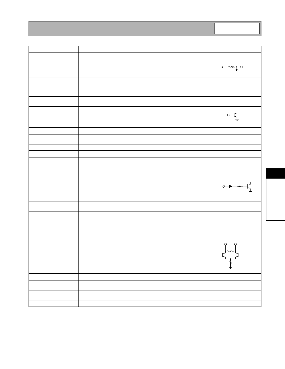
Pin
Function
Description
Interface Schematic
1
NC
No connection. This pin may be grounded (recommended) or left open.
2
VCC1
Supply voltage for the mixer and RF buffer amplifier. External RF
bypassing is required. The trace length between the pin and the bypass
capacitor should be minimized. The ground side of the bypass capaci-
tor should connect immediately to ground plane.
3
VCC2
Supply voltage for the LNA. External RF bypassing is required. The
trace length between the pin and the bypass capacitor should be mini-
mized. The ground side of the bypass capacitor should connect imme-
diately to ground plane.
4
GND1
Ground connection for the LNA. For best performance, keep traces
physically short and connect immediately to ground plane.
5
LNA IN
RF input pin for the LNA. This pin is internally matched for minimum
noise figure (NOT for minimum VSWR), given a 50
source imped-
ance. This pin is not internally DC-blocked.
6
GND2
Same as pin 4.
7
GND3
Ground connection for the RF buffer amplifier. For best performance,
keep traces physically short and connect immediately to ground plane.
8
NC
No connection. This pin may be grounded (recommended) or left open.
9
GND4
Same as pin 7.
10
VCC3
Supply voltage for both LO buffer amplifiers. External RF bypassing is
required. The trace length between the pin and the bypass capacitor
should be minimized. The ground side of the bypass capacitor should
connect immediately to ground plane.
11
LO BUFF
EN
Enable pin for the LO output buffer amplifier. This is a digitally con-
trolled input. A logic "high" (
3.1V) turns the buffer amplifier on, and the
current consumption increases by 3mA (with -2dBm LO input). A logic
"low" (
0.5V) turns the buffer amplifier off.
12
LO IN
Mixer LO input pin. This pin is internally DC-blocked and matched to
50
.
13
LO BUFF
OUT
Optional buffered LO output. This pin is internally DC-blocked and
matched to 50
. The buffer amplifier is switched on or off by the volt-
age level at pin 11.
14
GND5
Ground connection for both LO buffer amplifiers. For best performance,
keep traces physically short and connect immediately to ground plane.
15
IF+
Open-collector IF output pin. This is a balanced output. The output
impedance is set by an internal 1000
resistor to pin 16. Thus the dif-
ferential IF output impedance is 1000
. The resistor sets the operating
impedance, but an external choke or matching inductor to V
CC
must be
supplied in order to bias this output. This inductor is typically incorpo-
rated in the matching network between the output and IF filter. Because
this pin is biased to V
CC
, a DC blocking capacitor must be used if the IF
filter input has a DC path to ground.
16
IF-
Same as pin 15, except complementary output.
See pin 15.
17
GND6
Ground connection for the mixer. For best performance, keep traces
physically short and connect immediately to ground plane.
18
MIX RF IN
Mixer RF input pin. This pin is internally DC-blocked and matched to
50
.
19
GND7
Same as pin 17.
150
VCC1
VCC4
BIAS
LNA IN
7.5 k
LO BUFF EN
1 k
IF-
IF+
8-108
RF2486
Rev A7 010717
8
F
R
O
N
T
-
E
NDS
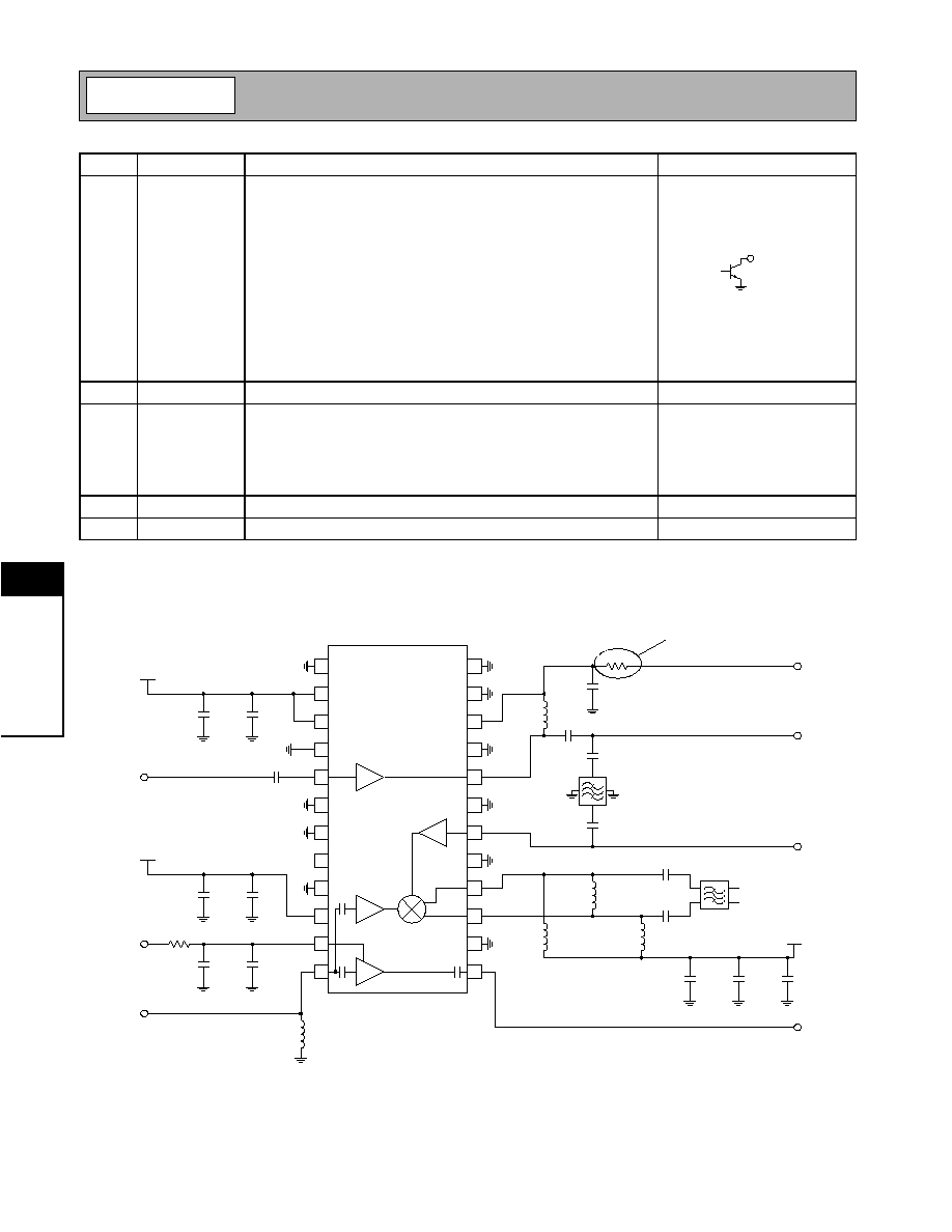
Application Schematic
1.96GHz, 210MHz IF
Pin
Function
Description
Interface Schematic
20
LNA OUT
LNA output pin. This is an open-collector output. This pin is typically
connected to pin 22 through a bias/matching inductor. This inductor, in
conjunction with a series blocking/matching capacitor, forms a match-
ing network to the 50
image filter and provides bias (see application
schematic). The LNA's IP3 may be increased 10dB by connecting pin
20 to V
CC
through the inductor. The LNA's current then increases by
10mA. Other in-between IP3 versus I
CC
trade-offs may be made by
connecting resistance values between V
CC
and the matching inductor.
The two reference points for consideration are with 150
used, which
is what connection to pin 22 achieves, the input IP3 is +5.5dBm and the
LNA I
CC
is 5mA. Using no resistance, the input IP3 is +15.5 dBm and
the LNA I
CC
is 15 mA. Desired operating points in between these val-
ues may be roughly interpolated.
21
GND8
Same as pin 17.
22
VCC4
Output supply voltage for the LNA output (pin 20). This pin is typically
connected to pin 20 through a bias/matching inductor (see application
schematic). External RF bypassing is required. The trace length
between the pin and the bypass capacitor should be minimized. The
ground side of the bypass capacitor should connect immediately to
ground plane.
See pin 2.
23
GND9
Same as pin 17.
24
NC
No connection. This pin may be grounded (recommended) or left open.
LNA OUT
1
2
3
4
5
6
7
8
9
10
11
12
24
23
22
21
20
19
18
17
16
15
14
13
2 pF
22 pF
BUF ENBL
1 k
100 pF
2.7 nH
R2
VCC
22 pF
4.7
µ
F
22 pF
LNA2 IN
1.8 nH
22 pF
MIX IN
LNA OUT
See evaluation
board
1 nF
22 pF
LO OUT
470 nH
470 nH
470 nH
100 pF
V
CC
SAW
Filter
IF SAW
Filter
1
2
LO IN
V
CC
1 nF
22 pF
22 pF
1 nF
V
CC
1 nF
22 pF

8-109
RF2486
Rev A7 010717
8
F
R
O
N
T
-
E
NDS
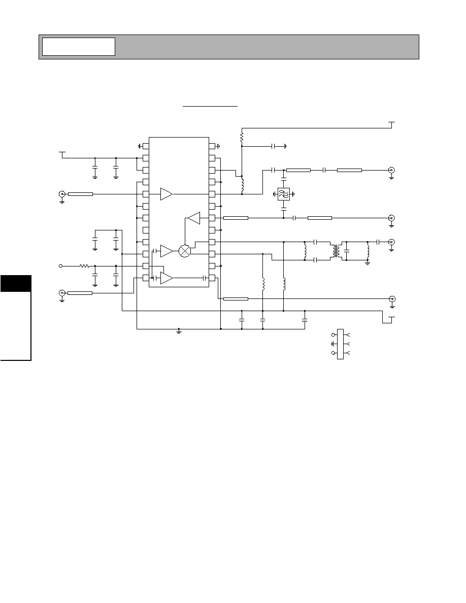
Evaluation Board Schematic
1.96GHz, 210MHz IF
(Download Bill of Materials from www.rfmd.com.)
1
2
3
4
5
6
7
8
9
1 0
1 1
1 2
2 4
2 3
2 2
2 1
2 0
1 9
1 8
1 7
1 6
1 5
1 4
1 3
C 1 2
2 2 p F
C 6
1 n F
5 0
µ
s trip
J 1
L N A 2 IN
B U F F E N
C 1 4
1 n F
C 7
2 2 p F
R 1
1 k
5 0
µ
s trip
J 2
L O IN
C 1 0
1 n F
C 5
2 2 p F
L 1
2 .7 n H
C 4
1 .5 p F
C 1 *
2 2 p F
C 2 *
2 2 p F
C 2 a
2 2 p F
F L 1 *
C 1 a
2 2 p F
5 0
µ
s trip
5 0
µ
s trip
J 6
L N A O U T
J 5
M IX E R IN
C 1 1
1 .0 p F
L 4
4 7 n H
C 8
5 p F
J 4
IF O U T
2 4 8 6 4 0 0 -
*C o m p o n e n ts n o t n o rm a lly p o p u la te d .
C 1 8
2 2 p F
NO TE S:
C 1 1 s e le c te d to fin e tu n e L 4 fo r IF o u tp u t m a tc h a t 2 1 0 M H z .
R 2 is n o rm a lly n o t p o p u la te d . F o r a p p lic a tio n s re q u irin g a d d itio n a l L N A IP 3 , s e e th e d a ta s h e e t fo r
re c o m m e n d e d r e s is ta n c e v a lu e s .
C 1 a a n d C 2 a a re n o rm a lly n o t p o p u la te d . If C 1 a a n d C 2 a a re p o p u la te d , th e L N A a n d m ix e r c a n b e
te s te d in d e p e n d e n tly . In th is c a s e , C 1 a n d C 2 s h o u ld b e re m o v e d .
T o u s e th e p a rt w ith o n b o a rd filte r, d o n o t p o p u la te C 1 a , a n d C 2 a .
U s e C 1 a n d C 2 in s te a d . T h is w ill a llo w c a s c a d e d o p e ra tio n o n ly .
P 1
1
2
3
B U F F E R E N A B L E
V C C
5 0
µ
s trip
V C C
* * S e e N o te s **
V C C
G n d
C 1 3
1 n F
C 9
2 2 p F
C 1 5
4 .7 u F
+
V
C C
L 2
4 7 0 n H
L 3
4 7 0 n H
5 0
µ
s trip
J 3
L O O U T
C 1 7
1 0 0 p F
L 5
2 2 0 n H
T 1
C 1 6
1 0 0 p F
T O K O
5 0
µ
s trip
**S e e N o te s **
5 0
µ
s trip
C 3
2 2 p F
R 2 *
S A T
* *S e e N o te s **
V
C C
V
C C
8-110
RF2486
Rev A7 010717
8
F
R
O
N
T
-
E
NDS
Evaluation Board Schematic
2.4GHz, 280MHz IF
(Download Bill of Materials from www.rfmd.com.)
1
2
3
4
5
6
7
8
9
10
11
12
24
23
22
21
20
19
18
17
16
15
14
13
C12
22 pF
C6
1 nF
50
µ
strip
J1
LNA2 IN
BUFF EN
C14
1 nF
C7
22 pF
R1
1 k
50
µ
strip
J2
LO IN
C10
1 nF
C5
22 pF
L1
1.8 nH
C4
2.0 pF
C1*
22 pF
C2*
22 pF
C2a
22 pF
FL1*
C1a
22 pF
50
µ
strip
50
µ
strip
J6
LNA OUT
J5
MIXER IN
C11
1.0 pF
L4
22 nH
C8
6 pF
J4
IF OUT
2486401-
*Components not normally populated.
NOTES:
C11 selected to Fine Tune L4 for IF Output Match at 280 MHz.
R2 is normally not populated. For applications requiring additional LNA IP3, see the datasheet for recommended resistance values.
C1a and C2a are normally not populated. If C1a and C2a are populated, the LNA and mixer can be tested independently.
In this case, C1 and C2 should be removed.
To use the part with onboard filter, do not populate C1a, and C2a.
Use C1 and C2 instead. This will allow cascaded operation only.
VCC
VCC
Gnd
C13
1 nF
C9
22 pF
V
CC
L2
470 nH
L3
470 nH
50
µ
strip
J3
LO OUT
C17
100 pF
L5
180 nH
C16
100 pF
50
µ
strip
**See Notes**
50
µ
strip
C3
22 pF
R2*
SAT
**See Notes**
V
CC
V
CC
T1
TOKO
GND
P1-3
VCC
P1-1
BUFFER ENABLE
P1
1
2
3
CON3
C15
4.7 uF
+
8-111
RF2486
Rev A7 010717
8
F
R
O
N
T
-
E
NDS
Evaluation Board Layout 1.96GHz
Board Size 3.0" x 3.0"
Board Thickness 0.075.6", Board Material FR-4, Multi-Layer
(8 mils between Layers 1 and 2, 31 mils between Layers 2 and 3, 1 ounce copper all layers)
8-112
RF2486
Rev A7 010717
8
F
R
O
N
T
-
E
NDS
Evaluation Board Layout 2.4GHz
Board Size 3.0" x 3.0"