NO
T
FOR
N
EW
DE
SI
GNS
12-1
Product Description
Ordering Information
Typical Applications
Features
Functional Block Diagram
RF Micro Devices, Inc.
7628 Thorndike Road
Greensboro, NC 27409, USA
Tel (336) 664 1233
Fax (336) 664 0454
http://www.rfmd.com
Optimum Technology MatchingÆ Applied
Si BJT
GaAs MESFET
GaAs HBT
Si Bi-CMOS
SiGe HBT
Si CMOS
InGaP/HBT
GaN HEMT
SiGe Bi-CMOS
1
2
3
4
8
7
6
5
VCC1
RES
GND1
NC
PD
GND2
RF OUT
VCC2
RF2504
VCO/HIGH-ISOLATION BUFFER AMPLIFIER
∑ 2-Way Paging
∑ ISM Band Systems
∑ Wireless Local Loop Systems
∑ GPS Receivers
∑ Cellular Systems
∑ Low Voltage Applications
The RF2504 is an integrated oscillator and buffer ampli-
fier chain designed to achieve extremely low sensitivity to
fluctuations in load impedance and power supply noise,
thereby greatly reducing load pulling and pushing. The IC
offers great flexibility, yet is easy to use. This product was
designed for use in applications with low supply voltages.
It has a power-down feature and is designed to operate
from 700MHz to 1500MHz with the help of an external
resonator. Frequency control is achieved with an external
varactor diode. The IC's ease of use, reduced load pull-
ing, small size, and low cost make it an ideal LO (Local
Oscillator) for almost any wireless application.
∑ High-Isolation/Reduced Load Pulling
∑ Low Current Consumption
∑ -6dBm Output Power
∑ Digitally Controlled Power Down Mode
∑ 700MHz to 1500MHz Operating Range
∑ Single 2.2V to 5V Supply
RF2504
VCO/High-Isolation Buffer Amplifier
RF2504 PCBA
Fully Assembled Evaluation Board
0
Rev A4 021007
0.244
0.229
0.157
0.150
0.018
0.014
0.050
0.068
0.053
NOTES:
1. Shaded lead is Pin 1.
2. All dimensions are excluding
mold flash.
3. Lead coplanarity -
0.005 with respect to datum "A".
0.196
0.189
0.008
0.004
-A-
8∞ MAX
0∞ MIN
0.034
0.016
0.009
0.007
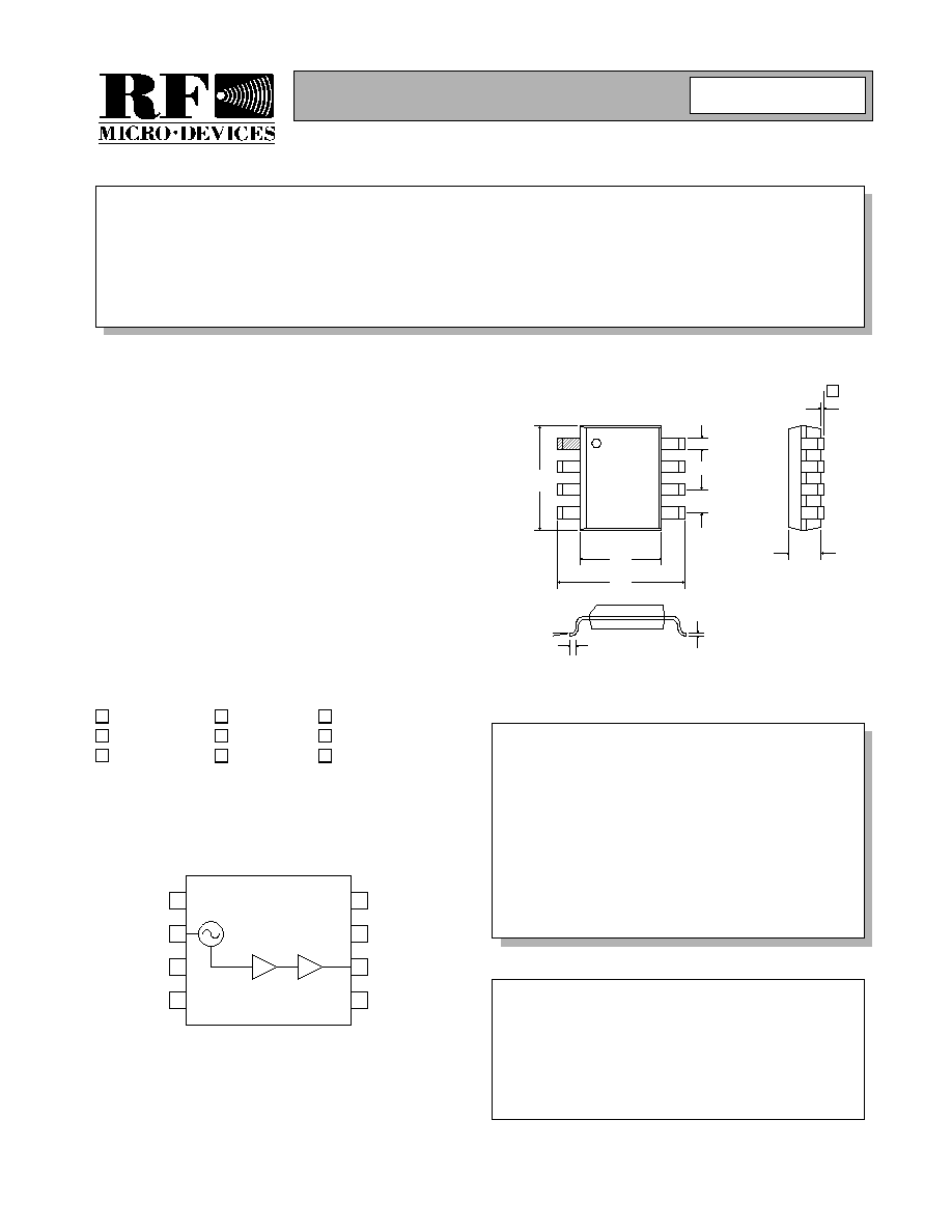
Package Style: SOIC-8
NOT FOR NEW DESIGNS
!

12-2
RF2504
Rev A4 021007
NO
T
FOR
N
EW
DE
SI
GNS
Absolute Maximum Ratings
Parameter
Rating
Unit
Supply Voltage
-0.5 to +5.8
V
DC
Power Down Voltage (V
PD
)
-0.5 to +5.8
V
DC
Operating Ambient Temperature
-40 to +85
∞C
Storage Temperature
-55 to +150
∞C
Parameter
Specification
Unit
Condition
Min.
Typ.
Max.
Overall
Operating Frequency
700 to 1500
MHz
915MHz Operation
T=25 ∞C, V
CC
=2.7V, Z
LOAD
=50
,
V
PD
=2.7V
Output Power
-6
dBm
2nd Harmonic
-8
dBc
3rd Harmonic
-19
dBc
Load Pulling
200
kHz
Into 1.67VSWR Load
V
CC
Pushing
4.7
MHz/V
Phase Noise
-104
dBc
100kHz Offset. Better phase noise is achiev-
able at the expense of output power.
-83
dBc
10kHz Offset
Power Supply
Operating Voltage
2.2 to 5.0
V
DC
At 2.2V and -40∞C, output power will be
reduced to typically -11dBm.
Supply Current
5.5
mA
Caution! ESD sensitive device.
RF Micro Devices believes the furnished information is correct and accurate
at the time of this printing. However, RF Micro Devices reserves the right to
make changes to its products without notice. RF Micro Devices does not
assume responsibility for the use of the described product(s).

12-3
RF2504
Rev A4 021007
NO
T
FOR
N
EW
DE
SI
GNS
Pin
Function
Description
Interface Schematic
1
VCC1
Power supply connection for the VCO. This pin should be well
bypassed close to the package with a capacitor suitable for the fre-
quency of operation as well as a capacitor to minimize low frequency
noise from the voltage supply. The ground side of the capacitors should
connect immediately to ground plane.
2
RES
Connection point for the resonator circuit. The resonator is an inductive
element. Changing the effective inductance, either physically or with a
varactor tuned circuit, will change the frequency of operation. Note that
all parasitics on the circuit board will contribute to the effective induc-
tance and will influence the frequency of operation. These effects
become more pronounced at higher operating frequencies. This pin
has DC bias present. A DC blocking capacitor, suitable for the fre-
quency of operation, should be used if the external circuitry has DC
present or presents a DC path to ground. See Application Example
Schematic and Theory of Operation section of this data sheet for
design details.
3
GND1
Ground connection for the VCO. Keep traces physically short and con-
nect immediately to ground plane for best performance. In order to min-
imize load pulling, it is recommended that pin 3 have a different return
path to ground than pin 7 (i.e., separate vias to a common ground
plane).
See Pin 2
4
NC
Not connected.
5
VCC2
Power supply connection for the buffer amplifiers. This pin should be
well bypassed close to the package with a capacitor suitable for the fre-
quency of operation. The ground side of the capacitor should connect
immediately to ground plane.
6
RF OUT
RF output pin. This is an open-collector output and must be biased
externally. A shunt bias/matching inductor to V
CC
and a series block-
ing/matching capacitor are recommended. See Application Example
Schematic.
7
GND3
Ground connection for the buffer amplifiers. Keep traces physically
short and connect immediately to ground plane for best performance.
In order to minimize load pulling, it is recommended that pin 3 have a
different return path to ground than pin 7 (i.e., separate vias to a com-
mon ground plane).
8
PD
Power Down pin for the VCO and buffer amplifiers. A logic "low" (0.0 to
0.7V) turns the entire device off and supply current drops to less than
1
µ
A. A logic "high" (
3.0V) turns the device on. Note that the voltage
on this pin should never exceed 5.5V
DC
.
Pins
3,4
Pin 2
To Buffer Amps
and Bias Ckts.
To Bias Ckts.

12-4
RF2504
Rev A4 021007
NO
T
FOR
N
EW
DE
SI
GNS
Application Notes
The RF2504 has two functional parts: an oscillator and
buffer amplifier. The functional blocks have separate
ground and VCC pins to increase the isolation and
reduce load pulling, one of the key design objectives.
An external resonator is used to add design flexibility,
and the loaded Q of this resonator will affect the perfor-
mance of the resulting oscillator.
To create an oscillation, negative resistance is gener-
ated at pin 2 with a circuit similar to a Colpitts oscillator.
The input impedance at pin 2, measured with a vector
network analyzer, is shown here in the data sheet. In
general, the impedance looks like a negative resis-
tance in series with a capacitor. The negative resis-
tance decays as the frequency increases. An oscillator
is created when an inductive element is placed on pin
2 that is the conjugate of the capacitive reactance. A
greater inductive element will create a lower frequency
of oscillation.
The S11 looking into pin 2 is also shown here in the
data sheet. It has return gain from 500 MHz to 2200
MHz at room temperature. The specified frequency
range of 750 MHz to 1500 MHz defines the region
where the output power is relatively flat. At lower and
higher frequencies, the power will tend to roll off from
the nominal value. The specified frequency range is
conservatively set to ensure oscillation and maintain
performance, but the RF2504 can be used over a
broader frequency range with degraded performance.
The overall Q of the external resonator will affect per-
formance. Lower Q means lower power, higher phase
noise, and more load pulling. If the Q is too low, the cir-
cuit will not oscillate. The IC is designed to oscillate
into a resonator with Q>10. The performance is mea-
sured with a microstrip resonator or high quality induc-
tor, which usually has a Q>50. These measurements
define the best performance that can be expected from
the ICs. Lower Q resonators, particularly those includ-
ing a lossy varactor, might have degraded perfor-
mance.
The specified output power is measured into a 50
load. The IC has a high output impedance, and if
desired, output matching can be used to obtain more
power by transforming 50
into a higher impedance.
On the RF2504, this could be accomplished by simply
changing the values of the external output inductor and
capacitor.
