 | –≠–ª–µ–∫—Ç—Ä–æ–Ω–Ω—ã–π –∫–æ–º–ø–æ–Ω–µ–Ω—Ç: RF2608 | –°–∫–∞—á–∞—Ç—å:  PDF PDF  ZIP ZIP |

¸
6-15
6
MI
X
E
R
S
Product Description
Ordering Information
Typical Applications
Features
Functional Block Diagram
RF Micro Devices, Inc.
7628 Thorndike Road
Greensboro, NC 27409, USA
Tel (336) 664 1233
Fax (336) 664 0454
http://www.rfmd.com
Optimum Technology MatchingÆ Applied
Si BJT
GaAs MESFET
GaAs HBT
Si Bi-CMOS
SiGe HBT
Si CMOS
1
IF+
2
IF-
3
GND
4
LO BYPASS
5
LO
6
GND
7
VCC
8
RF OUT
RF2608
CDMA/FM UPCONVERTER/BPSK MODULATOR
∑ CDMA/FM Cellular Systems
∑ Supports Dual-Mode AMPS/CDMA
∑ Supports Dual-Mode TACS/CDMA
∑ Commercial and Consumer Systems
∑ Battery-Operated Systems
The RF2608 is a complete upconverter designed for
CDMA/FM cellular applications. The IC contains a dou-
ble-balanced mixer stage and an output buffer amplifier
stage. This device may also be used to directly BPSK
modulate a carrier. The mixer is a Gilbert cell with emitter
degeneration resistors to provide high IP
3
. The output
stage is a class-B, push-pull configuration to reduce the
overall current and still provide a good 50
output match.
The unit operates at a supply voltage of 2.7 V to 5.0 V and
does not require any external matching components
other than coupling capacitors. This circuit is designed as
part of the RFMD CDMA chipset, consisting of a Transmit
IF AGC Amp, this Transmit Upconverter, a Receive LNA/
Mixer, and a Receive IF AGC Amp.
∑ Supports Dual Mode Operation
∑ +7dBm Output Intercept Point
∑ Single 2.7V to 5.0V Power Supply
∑ Internally Matched Inputs and Outputs
∑ Buffered Output
∑ Double-Balanced Mixer
RF2608
CDMA/FM Upconverter/BPSK Modulator
RF2608 PCBA
Fully Assembled Evaluation Board
6
Rev B3 010720
0.244
0.229
0.157
0.150
0.018
0.014
0.050
0.068
0.053
NOTES:
1. Shaded lead is Pin 1.
2. All dimensions are excluding
mold flash.
3. Lead coplanarity -
0.005 with respect to datum "A".
Dimensions in mm
0.196
0.189
0.008
0.004
-A-
8∞ MAX
0∞ MIN
0.034
0.016
0.009
0.007
Package Style: SOIC-8
6-16
RF2608
Rev B3 010720
6
MI
X
E
R
S
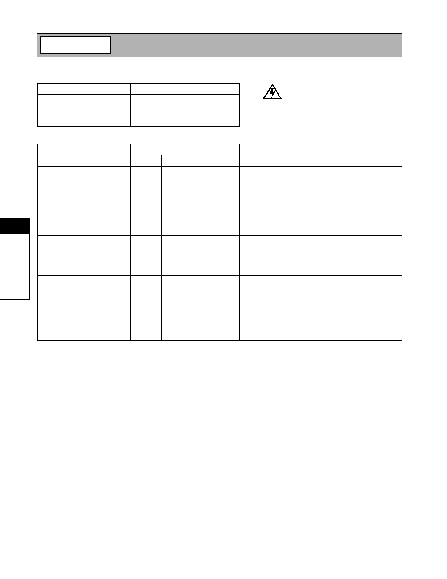
Absolute Maximum Ratings
Parameter
Rating
Unit
Supply Voltage
-0.5 to 7
V
DC
Input RF Power
+10
dBm
Operating Ambient Temperature
-40 to +85
∞C
Storage Temperature
-40 to +150
∞C
Parameter
Specification
Unit
Condition
Min.
Typ.
Max.
Overall
T = 25∞C, V
CC
=3.6V, RF= 840MHz,
LO= 970MHz @ -2 dBm, IF= 130MHz @ -12
dBm
RF Output Frequency Range
500
824 to 849
1500
MHz
Conversion Gain
-1.3
+0.5
+1.6
dB
Noise Figure
15
18
dB
Output IP3
+5
+7
dBm
Output VSWR
1.6:1
2.0:1
50
Spurious Product Rejection
30
dBc
Referenced to RF output
IF Input
IF Frequency
DC
130
200
MHz
Differential Input Impedance
215
265
315
IF to RF Output Isolation
21
23
dB
IF = 130MHz
IF to LO Isolation
40
50
dB
LO Input
LO Frequency Range
300
954 to 979
MHz
LO Level
-3 to +3
dBm
LO to RF Output Leakage
-28
-25
dBm
LO Input VSWR
<1.1:1
2.0:1
50
Power Supply
Voltage
2.7 to 5.0
V
Current Consumption
16
22
28
mA
V
CC
= 3.6V
Caution! ESD sensitive device.
RF Micro Devices believes the furnished information is correct and accurate
at the time of this printing. However, RF Micro Devices reserves the right to
make changes to its products without notice. RF Micro Devices does not
assume responsibility for the use of the described product(s).
6-17
RF2608
Rev B3 010720
6
MI
X
E
R
S
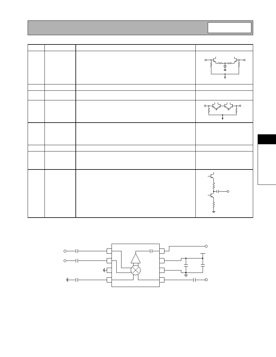
Application Schematic
Pin
Function
Description
Interface Schematic
1
IF+
Balanced IF input pin. This pin is internally DC-biased and should be
DC blocked if connected to a device with a DC level present. For single-
ended input operation, one pin is used as an input and the other IF
input is AC coupled to ground. The balanced, as well as single-ended,
input impedance is 265
. The IF input should be used differentially
when the part is used as a BPSK modulator.
2
IF-
Same as pin 1, except complementary input.
See pin 1.
3
GND
Ground connection. For best performance, keep traces physically short
and connect immediately to ground plane.
4
LO BYPASS
Bypass connection for the LO. A capacitor of 100pF to ground should
be connected to this pin
5
LO
Balanced LO input pin. This pin is internally DC-biased and should be
DC-blocked if connected to a device with a DC level present. For single-
ended input operation, one pin is used as an input and the other LO
input is AC-coupled to ground. The balanced, as well single-ended,
input impedance is 50
.
See pin 4.
6
GND
Same as pin 3.
7
VCC
Supply voltage pin. External bypassing is required. External RF, LO,
and IF bypassing is required. The trace length between the pin and the
bypass capacitors should be minimized. The ground side of the bypass
capacitors should connect immediately to ground plane.
8
RF OUT
RF output pin. This pin is internally DC-blocked. The output impedance
is 50
.
BIAS
IF-
IF+
BIAS
LO
BYPASS
LO
RF OUT
1
2
3
4
5
6
7
8
1 nF
IF+
1 nF
IF-
100 pF
100 pF
LO
RF OUT
100 pF
100 nF
V
CC

6-18
RF2608
Rev B3 010720
6
MI
X
E
R
S
Evaluation Board Schematic
(Download Bill of Materials from www.rfmd.com.)
Evaluation Board Layout
Board Size 1.420" x 1.420"
Board Thickness 0.031", Board Material FR-4
2608400A
1
2
3
4
5
6
7
8
C4
22 pF
C2
470 pF
T1
1:1
C1
470 pF
C3
4 pF
L1
100 nH
P1
1
2
3
NC
GND
P1-1
VCC
50
µ
strip
J1
IF IN
C5
22 pF
50
µ
strip
J2
LO IN
C6
47 pF
C7
100 nF
VCC
50
µ
strip
J3
RF OUT