6-1
Product Description
Ordering Information
Typical Applications
Features
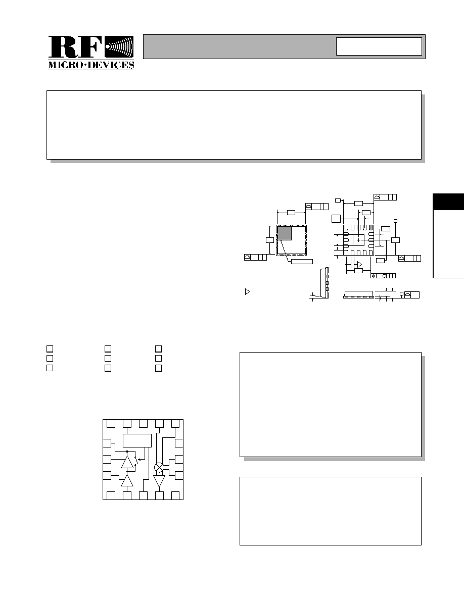
Functional Block Diagram
RF Micro Devices, Inc.
7628 Thorndike Road
Greensboro, NC 27409, USA
Tel (336) 664 1233
Fax (336) 664 0454
http://www.rfmd.com
Optimum Technology MatchingÆ Applied
Si BJT
GaAs MESFET
GaAs HBT
Si Bi-CMOS
!
SiGe HBT
Si CMOS
6
MI
XE
RS
GaInP/HBT
GaN HEMT
SiGe Bi-CMOS
MI
X
OU
T
PD
RF I
N
GND
GAIN
SELEC
T
VCC
LO+
LO-
GND
VP
A1
IF-
IF+
GND
RF OUT
RF GND2
RF GND1
16
15
14
13
12
11
10
9
7
8
5
6
3
4
1
2
Logic
Control
RF2642
3V 900MHz UPCONVERTER/
DRIVER AMPLIFIER WITH BYPASS MODE
∑ CDMA/AMPS Cellular Systems
∑ TDMA/AMPS Cellular Systems
∑ General Purpose Upconverter/Driver
∑ Portable Battery-Powered Equipment
The RF2642 is a complete upconverter and power ampli-
fier driver designed for CDMA applications. The design
features driver amplifier high and low gain states. In the
low gain state, the gain is adjustable and the device
draws less current. The upconverter is always on. The
power down mode turns off the driver amplifier. The
device features balanced IF inputs, single-ended LO
input and RF output for ease of interface. Packaged in an
industry standard 4mmx4mm, 16-pin, leadless chip car-
rier, the device provides a low-cost solution while easing
board space limitations.
∑ Single Supply 3.0V Operation
∑ Step Gain Control
∑ Power Down Control
∑ ACPR1=61dBc@885kHz with
P
OUT
=+5dBm
∑ Small Leadless LCC 16-Pin Package
RF2642
3V 900MHz Upconverter/ Driver Amplifier with
Bypass Mode
RF2642 PCBA
Fully Assembled Evaluation Board
6
Rev A6 020726
12∞
MAX
0.05
0.00
0.75
0.65
1.00
0.90
C
0.05
A
4.00
2.00
1.50
SQ.
4.00
2
2.00
1.60
2 PLCS
0.10 C A
2 PLCS
0.10
C A B
M
3.20
2 PLCS
0.75
0.50
3
0.45
0.28
INDEX AREA
0.10 C A
2 PLCS
3.75
3.75
0.10 C B
2 PLCS
0.10 C B
2 PLCS
-B-
0.80
TYP
Dimensions in mm.
NOTES:
1. Shaded pin is lead 1.
2. Pins 1 and 9 are fused.
1. Dimension applies to plated
terminal and is measured
between 0.10 mm and 0.25 mm
from terminal tip.
3
Package Style: LCC, 16-Pin, 4x4

6-2
RF2642
Rev A6 020726
6
MI
XE
RS
NOTE: The measured results do not include the losses from the IF balun and SAW filter. On the evaluation board, those
losses are as follows: IF Balun=1dB, SAW Filter=2.5dB to 3.5dB.
Absolute Maximum Ratings
Parameter
Rating
Unit
Supply Voltage
-0.5 to +4.5
V
DC
Input RF Power
+3
dBm
Operating Ambient Temperature
-30 to +85
∞C
Storage Temperature
-30 to +150
∞C
Parameter
Specification
Unit
Condition
Min.
Typ.
Max.
Overall
T=25∞C, V
CC
=3.0V, RF
OUT
=830MHz,
LO=960MHz@-3dBm, IF=130MHz
RF Output Frequency Range
824 to 849
MHz
IF Frequency Range
130
MHz
Output Power
+5
dBm
CW
High Gain Mode
GAIN SELECT=2.7V, V
PD
=2.7V
Gain
33
34.5
36
dB
Noise Figure
12
14
dB
IF Input Impedance
250
Differential @ 130MHz
RF Output VSWR
1.5
2:1
824MHz to 849MHz, external components
required
Current Consumption
52
mA
Adjacent Channel Power
Rejection (ACPR1)
55
61
dBc
P
OUT
=+5dBm, 885kHz offset
Alternate Channel Power
Rejection (ACPR2)
65
78
80
dBc
P
OUT
=+5dBm, 1.98MHz offset
Bypass Mode
GAIN SELECT=0V, V
PD
=2.7V
Gain
11.9
dB
Noise Figure
11.9
14
dB
IF Input Impedance
250
Differential @ 130MHz
RF Output VSWR
1.5
2:1
824MHz to 849MHz, external components
required
Output IP3
-4
+5.4
dBm
Current Consumption
26
mA
LO Input
954MHz to 979MHz
LO Frequency Range
954 to 979
MHz
LO Level
-6
-3
0
dBm
LO Input Impedance
50
LO to Mixer RF Output Leakage
-33
-20
dBm
LO Input VSWR
1.4
2:1
GAIN SELECT=0V
1.7
2:1
GAIN SELECT=2.7V
Power Supply
Voltage
2.7
3.0
3.3
V
Current Consumption
18
mA
V
PD
=0V
Caution! ESD sensitive device.
RF Micro Devices believes the furnished information is correct and accurate
at the time of this printing. However, RF Micro Devices reserves the right to
make changes to its products without notice. RF Micro Devices does not
assume responsibility for the use of the described product(s).

6-3
RF2642
Rev A6 020726
6
MI
XE
RS
Pin
Function
Description
Interface Schematic
1
GND
Ground connection. For best performance, keep traces physically short
and connect immediately to ground plane. This pin is internally con-
nected to the die flag.
2
RF OUT
Output match of the second stage of the power amplifier driver. This
amplifier output pin is open collector. It is matched to 50
externally
using a simple LC match. Refer to the application schematic.
3
RF GND2
The ground connection for the second stage of the power amplifier
driver. The inductance between this pin and the ground plane deter-
mines the gain of the second stage. Increased inductance results in
reduced gain.
On the evaluation board, the emitter ground inductance is set by the
length of the PCB trace connected between this pin and the ground. By
sliding a 0
ground jumper along this line, the inductance, and hence
the gain, may be varied.
The evaluation board is shipped with the 0
jumper very close to the
part, resulting in minimum inductance, and therefore maximum second
stage gain. This translates to higher output IP3 and maximum ACPR1.
This setting results in performance 6dB better than the ACPR1 mini-
mum specification of 50dBc in the CDMA IS-95 specification for a
P
OUT
=+5dBm.
4
RF GND1
The ground connection for the first stage of the power amplifier driver.
The inductance between this pin and the ground plane determines the
gain of the first stage. Increased inductance results in reduced gain.
On the evaluation board, the emitter ground inductance is set by the
length of the PCB trace connected between this pin and the ground. By
sliding a 0
ground jumper along this line, the inductance, and hence
the gain, may be varied.
The evaluation board is shipped with the 0
jumper far away from the
part, resulting in maximum inductance, and therefore minimum first
stage gain.
More gain may be obtained by shifting the 0
jumper toward the part.
A maximum total gain of 40dB may be achieved if the first stage is set
to minimum emitter inductor trace length.
See pin 3.
5
VPA1
Power supply pin for the first stage power amplifier. External compo-
nents provide tuning for the interstage match.
6
RF IN
RF input to the power amplifier. This input is DC-coupled, so an exter-
nal blocking capacitor is needed if the pin is connected to a DC path.
7
PD
Power Down control When this pin is low, the amplifier section of the IC
is shut off. When this pin is high, the amplifier section of the IC is turned
on. The upconverter portion of the IC remains on regardless of the
state of PD.
8
MIX OUT
Output for the upconverting mixer. This input is DC-coupled, so an
external blocking capacitor is needed if the pin is connected to a DC
path. The output impedance is 50
.
9
GND
Same as pin 1.
RF OUT
Gain
Select
PCB
Trace
VPA1
Bias
RF IN
MIX OUT

6-4
RF2642
Rev A6 020726
6
MI
XE
RS
*See parameter specifications for conditions.
Pin
Function
Description
Interface Schematic
10
IF-
Balanced IF Input Pin. This pin is internally DC-biased and should be
DC-blocked if connected to a device with a DC level present. For single-
ended input operation, one pin is used as an input and the other IF
input is AC coupled to ground. The input impedance is 250
in both
the balanced and single-ended modes.
11
IF+
Same as pin 10, except complementary input.
12
GND
Ground connection. For best performance, keep traces physically short
and connect immediately to ground plane.
13
LO-
Balanced LO Input Pin. This pin is internally DC-biased and should be
DC-blocked if connected to a device with a DC level present. For single-
ended input operation, one pin is used as an input and the other LO
input is AC coupled to ground. The input impedance is 50
in both the
balanced and single-ended modes.
14
LO+
Same as pin 13, except complementary input.
15
VCC
Supply voltage for all bias circuits and logic circuits.
16
GAIN
SELECT
When GAIN SELECT is high: the driver amplifier is switched to high
gain mode; both amplifier stages are active; the gain is maximized;
and, the entire device draws approximately 51mA. When GAIN
SELECT is low, the second stage of the PA driver is turned off and
bypassed. This results in a device current of 26mA, which is approxi-
mately a 50% current reduction. The upconverting mixer remains on in
both the high and low gain modes to prevent VCO pulling.
Pkg
Base
GND
Ground connection. The backside of the package should be soldered to
a top side ground pad which is connected to the ground plane with mul-
tiple vias.
PD
Gain
Select
Mixer
Amplifier
First Stage
Amplifier
Second Stage
Gain
(dB)*
0
0
ON
OFF
OFF
0
1
ON
OFF
OFF
1
0
ON
ACTIVE
BYPASSED
11.9
1
1
ON
ACTIVE
ACTIVE
34.5
BIAS
IF-
IF+
BIAS
LO
LO+

6-5
RF2642
Rev A6 020726
6
MI
XE
RS
Application Schematic
8
7
6
1
16
15
14
13
9
5
10
11
12
2
3
4
Logic
Control
10 nF
Gain Select
10 nF
VCC
1 nF
1 nF
1 nF
1 nF
1 nF
3.9 nH
8.2 nH
10 nF
VPA2
8.2 nH
10 nF
VPA1
PD
10 nF
1 nF
820
5.1
820
RF SAW
Filter
1 nF
2642400B
NOTE:
1. 1 nF: DC blocking capacitor - this can be removed if the filter is DC blocked.
2. T-attenuator - this is to control the overall gain of the upconverter + PA driver. This can be set to zero if it is desired.
See Note 2
PA OUT
Formed by stripline
RF GND2
Variable2
Formed by stripline
RF GND1
Variable1
See Note 1
IF+
IF-
LO IN
See Note 1