
5-71
5
MO
D
U
LA
T
O
R
S
A
N
D
UP
C
O
N
V
E
R
T
E
RS
Preliminary
Product Description
Ordering Information
Typical Applications
Features
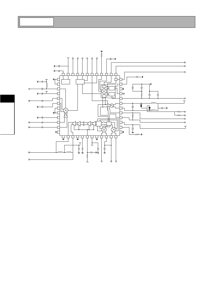
Functional Block Diagram
RF Micro Devices, Inc.
7625 Thorndike Road
Greensboro, NC 27409, USA
Tel (336) 664 1233
Fax (336) 664 0454
http://www.rfmd.com
Optimum Technology Matching� Applied
Si BJT
GaAs MESFET
GaAs HBT
Si Bi-CMOS
�
SiGe HBT
Si CMOS
Band Gap
Rel
Bias
Supply
Quad
/2
BG
V
CC3
MO
D
E
CE
TX
_
E
N
MI
X_
EN
VC
O
_
EN
P
LLO
N
PL
L
I
SET
VR
EF
PL
L
O
S
CRE
F
SET
1
48
45
46
47
44
43
42
41
40
39
38
37
NC
MO
D
O
U
T
-
MO
D
O
U
T
+
G
ND1
A
G
C_DE
C
VG
C
V
CC2
G
ND1
QS
I
G
QR
E
F
IRE
F
IS
IG
13
16
15
14
17
18
19
20
21
22
23
24
1
2
3
4
5
6
7
8
9
10
11
12
NC
NC
RFOUT
VCC4
LO2+
LO2-
GND2
GND2
MIX_DEC
MIX IN+
MIX IN-
NC
36
35
34
33
32
31
30
29
28
27
26
25
SET2
PLLVCC
PLLGND
LD
DO
VCO+
VCO-
LO1+
LO1-
VCC1
VCO_ISET
NC
Lock
Detect
/R
/N
Charge
Pump
RF2668
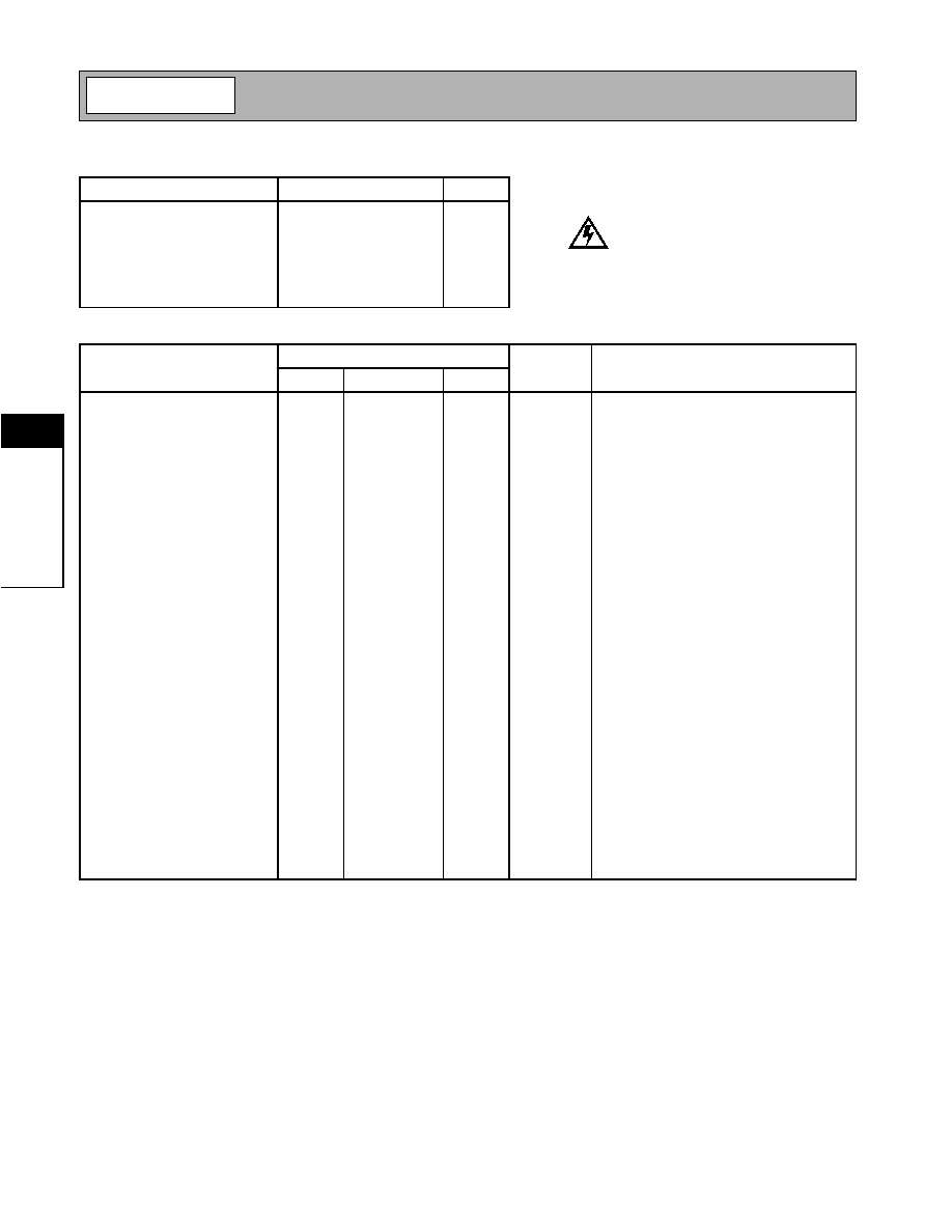
CDMA/FM TRANSMIT MODULATOR, IF AGC,
AND UPCONVERTER WITH INTEGRATED PLL
� CDMA/FM Cellular and PCS Systems
� Tri-Mode/Dual-Band CDMA Applications
� W-CDMA Systems
� Wireless Local Loop Systems
� Spread-Spectrum Cordless Phones
� High Speed Data Modems
The RF2668 is an integrated complete quadrature modu-
lator, IF AGC amplifier, upconverter, and PLL, designed
for the transmit section of dual-mode CDMA/FM cellular,
PCS, and tri-mode CDMA applications. It is designed to
modulate baseband I and Q signals, amplify the resulting
IF signals while providing 95dB of gain control range, and
perform the final upconversion to UHF. Noise Figure, IP
3
,
and other specifications are designed to be compatible
with the IS-98 Interim Standard. This circuit is designed
as part of RFMD's newest CDMA chipset, which also
includes the RF2667 CDMA/FM Receive IF AGC and
Demodulator. The IC is manufactured on an advanced
18GHz F
T
Silicon Bipolar process, and is supplied in a
48-lead plastic LQFP package.
� Supports Tri-Mode Operation
� Digitally Controlled Power Down Modes
� 2.7V to 3.3V Operation
� Digital First LO Quadrature Divider
� Double-Balanced UHF Upconvert Mixer
� IF AGC Amp with 95dB Gain Control
RF2668
CDMA/FM Transmit Modulator, IF AGC, and
Upconverter with Integrated PLL
RF2668 PCBA-PCS/CEL
Fully Assembled Evaluation Boards
RF2668 PCBA-DO
Fully Assembled Evaluation Boards
5
Rev B4 010423
9.00
+ 0.20
sq.
0.22
+ 0.05
7.00
+ 0.10 sq.
7� MAX
0� MIN
0.35
0.25
0.50
1.40
+ 0.05
0.127
0.60
0.15
0.10
+
Package Style: LQFP-48_7x7
Preliminary
5-72
RF2668
Rev B4 010423
5
MO
D
U
LA
T
O
R
S
A
N
D
UP
C
O
N
V
E
R
T
E
RS
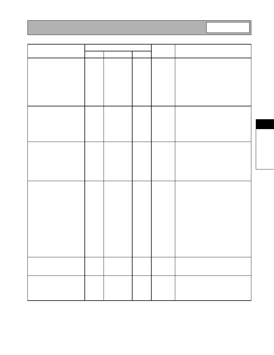
Absolute Maximum Ratings
Parameter
Rating
Unit
Supply Voltage
-0.5 to +5
V
DC
Power Down Voltage (V
PD
)
-0.5 to V
CC
+ 0.7
V
I and Q Levels, per pin
1
V
PP
LO1 Level, balanced
+6
dBm
Operating Ambient Temperature
-40 to +85
�C
Storage Temperature
-40 to +150
�C
Parameter
Specification
Unit
Condition
Min.
Typ.
Max.
I/Q Modulator & AGC
T = 25 �C, V
CC
=3.0V, Z
LOAD
= 200
,
LO1= -10dBm @ 260MHz, IF= 130MHz,
I SIG= Q SIG= 300mV
PP
,
RF Output externally matched
I/Q Input Frequency Range
0 to 20
MHz
Balanced
I/Q Input Impedance
80
k
Balanced
I/Q Input Reference Level
1.3
V
DC
Per Pin
LO1/FM Frequency Range
0
800
MHz
LO1/FM Input Level
-15
-10
-5
dBm
LO1/FM Input Impedance
200
Balanced
Sideband Suppression
35
40
dBc
I/Q Amplitude adjusted to within
�
20mV
27
dBc
Unadjusted
Carrier Suppression
40
50
dBc
I/Q DC Offset adjusted to within
�
20mV
30
dBc
Unadjusted
Max Output, FM Mode
+2.5
+5
dBm
V
GC
= 2.4V
DC
, T = -20�C to +85�C
Max Output, CDMA Mode
-3
0
dBm
V
GC
= 2.4V
DC
, T = -20�C to +85�C,
IS-95A CDMA Modulation
-2
0
dBm
ISIG= QSIQ= 300mVpp@ 100kHz
Min Output, CDMA Mode
-95
-89
dBm
V
GC
= 0.3V
DC
, T = -20�C to +85�C,
IS-95A CDMA Modulation
Output Power Accuracy
-3
+3
dB
T=-20 to +85 �C, Ref=25 �C
-2
+2
dB
1.4V
GC
2.5
Adjacent Channel Power Rejec-
tion @ 885kHz
-60
dBc
IS-95A CDMA Modulation
P
OUT
= -5dBm
Adjacent Channel Power Rejec-
tion @ 1.98MHz
-69
dBc
IS-95A CDMA Modulation
P
OUT
= -5dBm
Output Noise Power
-117
-111
dBm/Hz
P
OUT
= -1dBm, T=-20�C to +85�C
Output Impedance
200
Balanced
Current Consumption
40
mA
I/Q modulator and AGC only.
Caution! ESD sensitive device.
RF Micro Devices believes the furnished information is correct and accurate
at the time of this printing. However, RF Micro Devices reserves the right to
make changes to its products without notice. RF Micro Devices does not
assume responsibility for the use of the described product(s).
Preliminary
5-73
RF2668
Rev B4 010423
5
MO
D
U
LA
T
O
R
S
A
N
D
UP
C
O
N
V
E
R
T
E
RS
Parameter
Specification
Unit
Condition
Min.
Typ.
Max.
UHF Upconverter
Output externally matched
General
IF Input Impedance
200
Balanced
IF Input Frequency Range
0
400
MHz
LO2 Input Impedance
50
Single Ended
LO2 Input Level
-6
-3
0
dBm
LO2 Input Frequency Range
2.5
GHz
RF to LO2 Isolation
30
dB
LO Input VSWR
<2:1
50
Current Consumption
24
mA
UHF upconverter only.
Cellular
Conversion Gain
-1.5
-0.5
dB
RF
OUT
= 830MHz
Noise Figure (SSB)
15
dB
RF
OUT
= 830MHz
Output IP3
+13
dBm
P
IN
= -15dBm per tone,
200kHz tone separation, RF
OUT
= 830MHz,
LO2= 960MHz@ -3dBm
RF Output VSWR
<2:1
RF
OUT
= 830MHz
W-CDMA
Conversion Gain
-1.5
dB
RF
OUT
= 1950MHz
Noise Figure
TBD
dB
Output IP3
10
dBm
P
IN
= -15dBm per tone,
200kHz tone separation, RF
OUT
= 1950MHz,
LO2=1570MHz @-3dBm
RF Output VSWR
<2:1
RF
OUT
= 1950MHz. See note on eval board
schematic.
Dual Output
Cellular
Conversion Gain
-1.5
-0.5
dB
RF
OUT
= 830MHz
Noise Figure
15
dB
RF
OUT
= 830MHz
Output IP3
12.5
dBm
P
IN
= -15dBm per tone,
200kHz tone separation, RF
OUT
= 830MHz,
LO2= 960MHz@-3dBm
RF Output VSWR
<1.5:1
RF
OUT
= 830MHz
PCS
Conversion Gain
-1.5
-1.0
dB
RF
OUT
= 1880MHz
Noise Figure
15
dB
RF
OUT
= 1880MHz
Output IP3
10.5
dBm
P
IN
= -15dBm per tone,
200kHz tone separation, RF
OUT
= 1880MHz,
LO2=1750MHz @-3dBm
RF Output VSWR
<1.5:2
RF
OUT
= 1880MHz
VCO
PLL locked with Loop BW =5kHz, Tank Val-
ues: 39nH and SMV1234 varactor.
Phase Noise @ 100kHz
-110
dBc/Hz
Current Consumption
1
mA
PLL
Charge Pump Current
100
�
A
TCXO Input Level
0.8
V
PP
PLL Lock Time
4/Loop BW
s
Current Consumption
4
mA
PLL only.
Preliminary
5-74
RF2668
Rev B4 010423
5
MO
D
U
LA
T
O
R
S
A
N
D
UP
C
O
N
V
E
R
T
E
RS
Parameter
Specification
Unit
Condition
Min.
Typ.
Max.
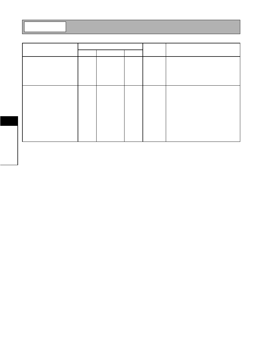
Power Supply
Supply Voltage
2.7
3.0
3.3
V
Current Consumption
69
mA
Total device current.
Power Down Current
<10
�
A
VPD HIGH Voltage
V
CC
-0.3
V
VPD LOW Voltage
0.3
V
PLL Settings
Application
Japan
Japan
US/Korea
LO Frequency, MHz
333.7
333.7
260.76
IF Frequency =LO Frequency/2
Crystal, MHz
19.2
19.8
19.68
Reference Divider
192
198
252
Phase Detector Frequency, kHz
100
100
78.09524
Prescaler
32/33
32/33
32/33
Swallow Counter (A)
9
9
11
Fixed Divider (N)
104
104
104
Net N in VCO Path
3337
3337
3339
SET1
VCC
GND
GND
SET2
GND
VCC
GND
Preliminary
5-75
RF2668
Rev B4 010423
5
MO
D
U
LA
T
O
R
S
A
N
D
UP
C
O
N
V
E
R
T
E
RS
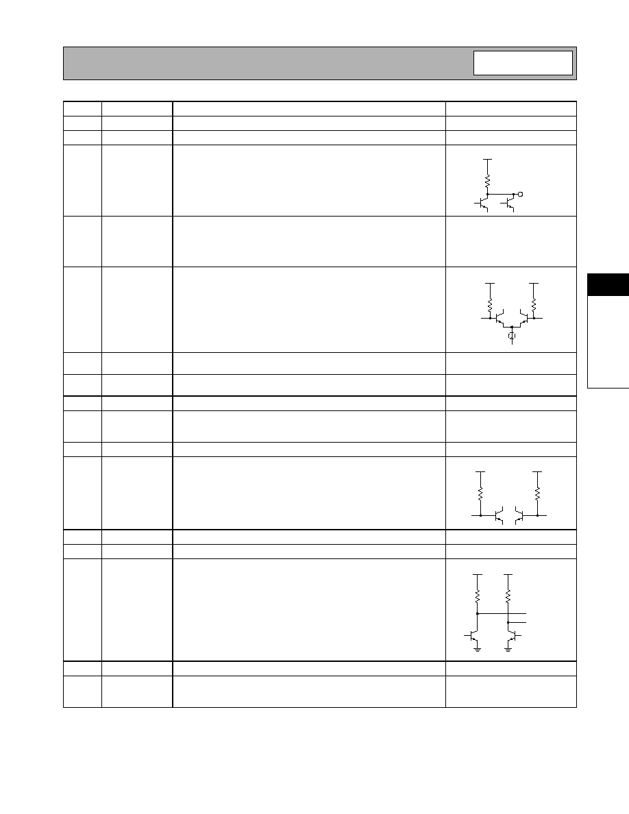
Pin
Function
Description
Interface Schematic
1
NC
Not connected.
2
NC
Not connected.
3
RF OUT
RF output pin. An external shunt inductor to V
CC
plus a series blocking/
matching capacitor are required for 50
output.
4
VCC4
Supply for the mixer stage only. The supply for the mixer is separated to
maximize IF to RF isolations and reduce the carrier leakage. A 10nF
external bypass capacitor is required. The trace length between the pin
and the bypass capacitors should be minimized. The ground side of the
bypass capacitors should connect immediately to ground plane.
5
LO2+
One half of the balanced mixer LO2 input. In single-ended applications,
the other half of the input, LO2- is AC grounded. This is a 50
imped-
ance port. This pin is NOT internally DC-blocked. An external blocking
capacitor (100pF recommended) must be provided if the pin is con-
nected to a device with DC present.
6
LO2-
One half of the balance mixer LO2 input. In single ended applications,
this pin is AC grounded with a 100pF capacitor.
See pin 5.
7
GND2
Ground connection for the mixer stage. For best performance, keep
traces physically short and connect immediately to ground plane.
8
GND2
Same as pin 7.
9
MIX_DEC
Current Mirror decoupling pin. A 1000pF external capacitor is required
to bypass this pin. The ground side of the bypass capacitors should
connect immediately to ground plane.
10
MIX IN+
Same as pin 11, except complementary input.
See pin 11.
11
MIX IN-
One half of the 200
balanced impedance input to the mixer stage.
This pin is NOT internally DC-blocked. An external blocking capacitor
(1000pF recommended) must be provided if the pin is connected to a
device with DC present. If no IF filter is needed this pin may be con-
nected to MOD OUT+ through a DC blocking capacitor. An appropriate
matching network may be needed if an IF filter is used.
12
NC
Not connected.
13
NC
Not connected.
14
MOD OUT-
One half of the balanced AGC output port. The impedance of this port
is 200
balanced. If no filtering is required, this pin can be connected
to the MIX IN- pin through a DC blocking capacitor. This pin requires an
inductor to V
CC
to achieve full dynamic range. In order to maximize
gain, this inductor should be a high-Q type and should be parallel reso-
nated out with a capacitor (see application schematic). This pin is NOT
DC-blocked. A blocking capacitor of 2200pF is needed when this pin is
connected to a DC path. An appropriate matching network may be
needed if an IF filter is used.
15
MOD OUT+
Same as pin 14, except complementary output.
See pin 14.
16
GND1
Ground connection for all baseband circuits including bandgap, AGC,
flip-flop, modulator and FM amp. For best performance, keep traces
physically short and connect immediately to ground plane.
RF OUT
300
V
CC4
50
BIAS
50
BIAS
LO2+
LO2-
100
BIAS
100
BIAS
MIX IN-
MIX IN+
100
100
MOD OUT-
MOD OUT+
V
CC3
V
CC3
Preliminary
5-76
RF2668
Rev B4 010423
5
MO
D
U
LA
T
O
R
S
A
N
D
UP
C
O
N
V
E
R
T
E
RS
Pin
Function
Description
Interface Schematic
17
AGC_DEC
AGC decoupling pin. An external bypass capacitor of 1nF capacitor is
required. The trace length between the pin and the bypass capacitors
should be minimized. The ground side of the bypass capacitors should
connect immediately to ground plane.
18
VGC
Analog gain control for AGC amplifiers. Valid control voltage ranges are
from 0.3V
DC
to 2.4V
DC
. The gain range for the AGC is 95dB. These
voltages are valid ONLY for a 39k
source impedance. A DC voltage
less than or equal to the maximum allowable V
CC
may be applied to
this pin when no voltage is applied to the V
CC
pins.
19
VCC2
Supply for the modulator stage only. A 10nF external bypass capacitor
is required and an additional 0.1
�
F will be required if no other low fre-
quency bypass capacitors are nearby. The trace length between the pin
and the bypass capacitors should be minimized. The ground side of the
bypass capacitors should connect immediately to ground plane.
20
GND1
Same as pin 16.
21
Q SIG
Baseband input to the Q mixer. This pin is DC-coupled. The DC level of
1.3V must be supplied to this pin to bias the transistor. Input imped-
ance of this pin is 50k
minimum. A DC voltage less than or equal to
the maximum allowable V
CC
may be applied to this pin when no voltage
is applied to the V
CC
pins.
22
Q REF
Reference voltage for the Q mixer. This voltage should be the same as
the DC voltage supplied to the Q SIG pin. For maximum carrier sup-
pression, DC voltage on this pin relative to the Q SIG DC voltage may
be adjusted. Input impedance of this pin is 50k
minimum. A DC volt-
age less than or equal to the maximum allowable V
CC
may be applied
to this pin when no voltage is applied to the V
CC
pins.
See pin 21.
23
I REF
Reference voltage for the I mixer. This voltage should be the same as
the DC voltage supplied to the I SIG pin. For maximum carrier suppres-
sion, DC voltage on this pin relative to the I SIG DC voltage may be
adjusted. Input impedance of this pin is 50k
minimum. A DC voltage
less than or equal to the maximum allowable V
CC
may be applied to
this pin when no voltage is applied to the V
CC
pins.
See pin 24.
24
I SIG
Baseband input to the I mixer. This pin is DC coupled. The DC level of
1.3V must be supplied to this pin to bias the transistor. Input imped-
ance of this pin is 50k
minimum. A DC voltage less than or equal to
the maximum allowable V
CC
may be applied to this pin when no voltage
is applied to the V
CC
pins.
25
NC
Not connected.
26
VCO_ISET
An external resistor of 47k
is used to set the VCO current for mini-
mum phase noise.
27
VCC1
Supply Voltage for the LO1 flip-flop and limiting amp only. This supply is
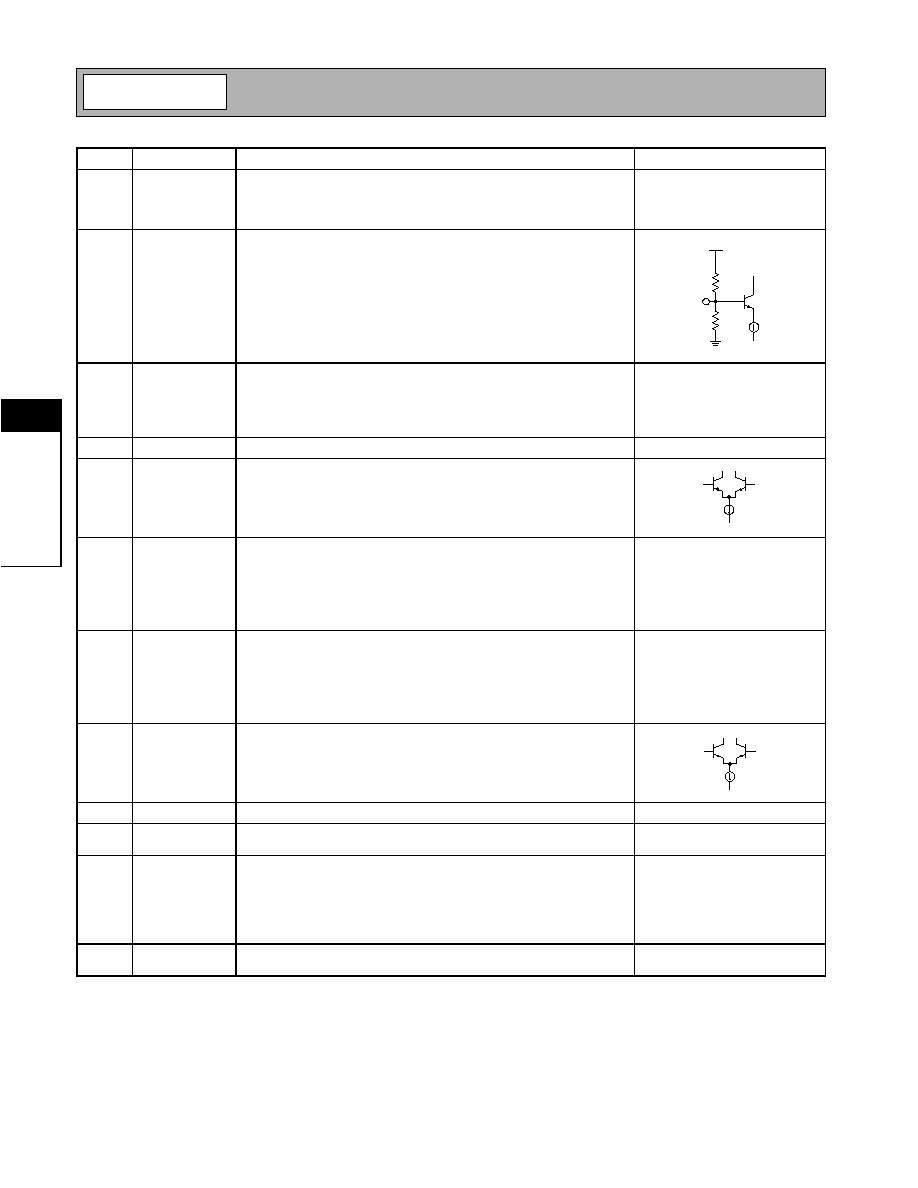
isolated to minimize the carrier leakage. A 1nF external bypass capaci-
tor is required, and an additional 0.1
�
F will be required if no other low
frequency bypass capacitors are nearby. The trace length between the
pin and the bypass capacitors should be minimized. The ground side of
the bypass capacitors should connect immediately to ground plane.
28
LO1-
External LO input to modulator. Controlled by VCO_EN signal. Logic
low is internal VCO, while logic high is external VCO.
See pin 29.
21 k
GC
40 k
BIAS
Q SIG
Q REF
I SIG
I REF
Preliminary
5-77
RF2668
Rev B4 010423
5
MO
D
U
LA
T
O
R
S
A
N
D
UP
C
O
N
V
E
R
T
E
RS
Pin
Function
Description
Interface Schematic
29
LO1+
External LO input to modulator. Controlled by VCO_EN signal. Logic
low is internal VCO, while logic high is external VCO.
30
VCO-
See VCO+ description.
31
VCO+
This port is used to supply DC voltage to the VCO as well as to tune the
center frequency of the VCO. Equal value inductors should be con-
nected to this pin and pin 30 although a small imbalance can be used
to tune in the proper frequency range.
32
DO
Output of the charge pump, and input to the VCO control. An RC net-
work from this pin to ground is used to establish the PLL bandwidth.
33
LD
Lock detector output for synthesizer. Requires external transistor to
provide hysteresis and inversion of signal. See Application circuit.
34
PLLGND
Ground for synthesizer. For best performance, keep traces physically
short and connect immediately to ground plane.
35
PLLVCC
Supply for the PLLVCC only. A 10nF external bypass capacitor is
required and an additional 0.1
�
F will be required if no other low fre-
quency bypass capacitors are nearby. The trace length between the pin
and the bypass capacitors should be minimized. The ground side of the
bypass capacitors should connect immediately to ground plane.
36
SET2
PLL Setting (Divider) pin. See the PLL settings table.
37
SET1
Same as pin 36.
38
OSCREF
TCXO reference input for synthesizer.
39
VREFPLL
Bypass pin for the synthesizer reference voltage.
40
PLLISET
Current setting pin for synthesizer charge pump. For normal operation,
a 390
resistor to ground should be used to set the current.
41
PLLON
Synthesizer Enable pin.
See pin 45.
42
VCO_EN
VCO Enable pin. Switches between internal and external VCO.
See pin 45.
43
MIX_EN
Power down control for mixer only. When connected to logic "high"
(>V
CC
-0.3) the mixer circuits are operating; when connected to ground
(
0.3V), the mixer is turned off but all other circuits are operating. A DC
voltage less than or equal to the maximum allowable V
CC
may be
applied to this pin when no voltage is applied to the V
CC
pins.
44
TX_EN
Shuts down the entire TX path. VCO is still active when TX disabled.
Logic high (>V
CC
-0.3) for TX Enable.
45
CE
Power down control for overall circuit. When logic "high" (
V
CC
-0.3V),
all circuits are operating; when logic "low" (
0.3V), all circuits are
turned off. The input impedance of this pin is >10k
. A DC voltage less
than or equal to the maximum allowable Vcc may be applied to this pin
when no voltage is applied to the V
CC
pins.
46
MODE
Selects between CDMA and FM mode. This is a digitally controlled
input. A logic "high" (
V
CC
-0.3V
DC
) selects CDMA mode. A logic "low"
(
<
0.3V
DC
) selects FM mode. In FM mode, this switch enables the FM
amplifier and turns off the I&Q modulator. The impedance on this pin is
30k
. A DC voltage less than or equal to the maximum allowable V
CC
may be applied to this pin when no voltage is applied to the V
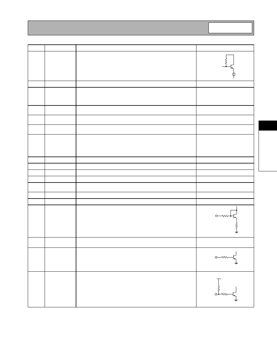
CC
pins.
1 k
LO1+, FM+
1 k
MIX EN
450
10 k
CE
60 k
60 k
BIAS
MODE
Preliminary
5-78
RF2668
Rev B4 010423
5
MO
D
U
LA
T
O
R
S
A
N
D
UP
C
O
N
V
E
R
T
E
RS
Pin
Function
Description
Interface Schematic
47
VCC3
Supply voltage for the AGC and the Bandgap circuitry. A 1nF external
bypass capacitor is required and an additional 0.1
�
F will be required if
no other low frequency bypass capacitors are nearby. The trace length
between the pin and the bypass capacitors should be minimized. The
ground side of the bypass capacitors should connect immediately to
ground plane.
48
BG OUT
Bandgap voltage reference. This voltage, constant over temperature
and supply variation, is used to bias internal circuits. A 1nF external
bypass capacitor is required.
Preliminary
5-79
RF2668
Rev B4 010423
5
MO
D
U
LA
T
O
R
S
A
N
D
UP
C
O
N
V
E
R
T
E
RS
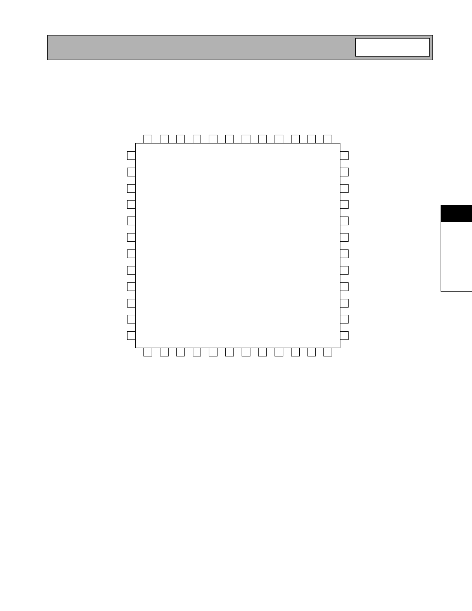
Pin-Out
BG
VCC3
MO
D
E
CE
TX
_E
N
MIX_
EN
VCO
_
EN
P
LLON
P
LLI
S
E
T
VREF
PL
L
O
S
CREF
SET
1
48
45
46
47
44
43
42
41
40
39
38
37
NC
M
O
D
O
UT
-
M
O
D
O
UT
+
G
ND1
AG
C_DEC
VG
C
VCC2
G
ND1
QS
I
G
QR
E
F
IR
EF
ISIG
13
16
15
14
17
18
19
20
21
22
23
24
1
2
3
4
5
6
7
8
9
10
11
12
NC
NC
RFOUT
VCC4
LO2+
LO2-
GND2
GND2
MIX_DEC
MIX IN+
MIX IN-
NC
36
35
34
33
32
31
30
29
28
27
26
25
SET2
PLLVCC
PLLGND
LD
DO
VCO+
VCO-
LO1+
LO1-
VCC1
VCO_ISET
NC
Preliminary
5-80
RF2668
Rev B4 010423
5
MO
D
U
LA
T
O
R
S
A
N
D
UP
C
O
N
V
E
R
T
E
RS
Application Schematic
Single- or Dual-Mode Operation
Band Gap
Rel
Bias
Supply
Quad
/2
48
45
46
47
44
43
42
41
40
39
38
37
13
16
15
14
17
18
19
20
21
22
23
24
1
2
3
4
5
6
7
8
9
10
11
12
36
35
34
33
32
31
30
29
28
27
26
25
12 nH
2 pF
10 nF
10 nF
100 pF
100 pF
1 nF
1 nF
1 nF
1 nF
10 nF
MODE CE
AGC
MIX
EN
VCO
EN
PLL
ON
270
1 nF
SET1
SET2
47 k
10 nF
200
D1
39 nH
**
39 nH
**
10 nF
3.9 k
VTUNE
DO
LD
10 nF
36 k
1 nF
220 pF
DO
10 nF
1 nF
1 nF
39 k
10 nF
10 nF
REF
Lock
Detect
/R
/N
Charge
Pump
V
CC
V
CC
V
CC
RF OUT
LO2
MIX IN+
MOD OUT-
V
CC
V
GC
OSIG
ISIG
V
CC
LO1+
V
CC
OSC REF
2.2 nF
33 pF
LO1-
MIX IN-
MOD OUT+
V
CC
L1*
L2*
*L1 and L2 are the bias
choke inductor.
**Denotes components not normally populated.
Preliminary
5-81
RF2668
Rev B4 010423
5
MO
D
U
LA
T
O
R
S
A
N
D
UP
C
O
N
V
E
R
T
E
RS
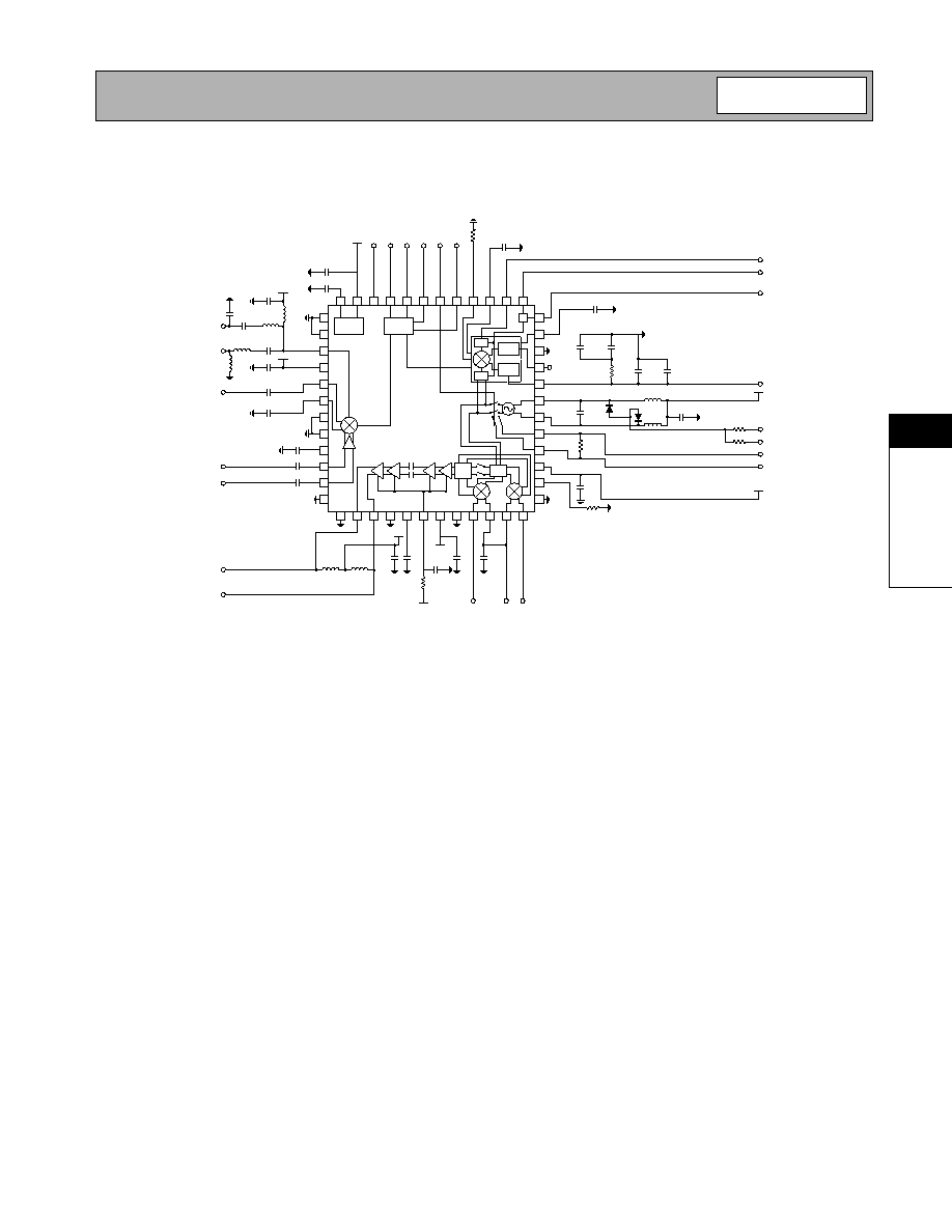
Application Schematic
Tri-Mode/Dual-Band Operation
Band Gap
Rel
Bias
Supply
Quad
/2
48
45
46
47
44
43
42
41
40
39
38
37
13
16
15
14
17
18
19
20
21
22
23
24
1
2
3
4
5
6
7
8
9
10
11
12
36
35
34
33
32
31
30
29
28
27
26
25
12 nH
0.5 pF
10 nF
10 nF
100 pF
100 pF
1 nF
1 nF
1 nF
1 nF
10 nF
MODE CE
AGC
MIX
EN
VCO
EN
PLL
ON
270
1 nF
SET1
SET2
47 k
10 nF
D1
39 nH
**
39 nH
**
10 nF
3.9 k
VTUNE
DO
LD
10 nF
36 k
1 nF
220 pF
DO
1 nF
1 nF
39 k
10 nF
10 nF
REF
Lock
Detect
/R
/N
Charge
Pump
V
CC
V
CC
V
CC
RF OUT (PCS)
LO2
MIX IN+
V
CC
V
GC
OSIG
ISIG
V
CC
V
CC
OSC REF
2.2 nF
33 pF
8.2 nH
3.9 nH
8 nH
4.7 pF
4.7 pF
RF OUT (CELL)
MIX IN-
10 nF
MOD OUT-
MOD OUT+
V
CC
L1*
L2*
*L1 and L2 are the bias
choke inductor.
200
LO1+
LO1-
**Denotes components not normally populated.
Preliminary
5-82
RF2668
Rev B4 010423
5
MO
D
U
LA
T
O
R
S
A
N
D
UP
C
O
N
V
E
R
T
E
RS
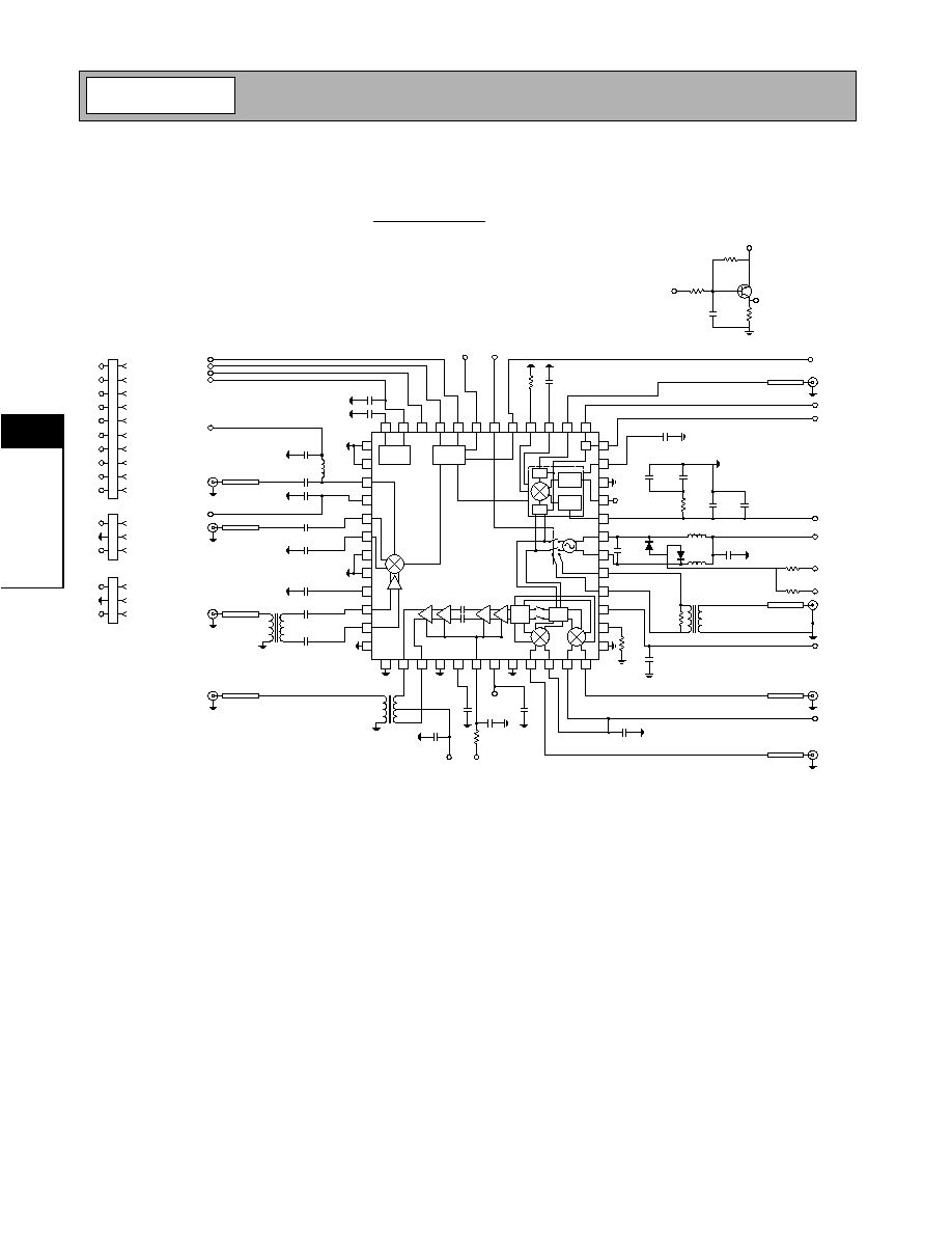
Evaluation Board Schematic
RF
OUT
=830MHz
(Download Bill of Materials from www.rfmd.com.)
Band Gap
Rel
Bias
Supply
Quad
/2
48
45
46
47
44
43
42
41
40
39
38
37
13
16
15
14
17
18
19
20
21
22
23
24
1
2
3
4
5
6
7
8
9
10
11
12
36
35
34
33
32
31
30
29
28
27
26
25
L1
12 nH
C3
2 pF
50
�
strip
J1
RF OUT
VCC
C18
10 nF
VCC
C5
100 pF
50
�
strip
J2
LO2
C6
100 pF
C9
1 nF
T1
T4-1
50
�
strip
J3
MIX IN
C8
1 nF
C7
1 nF
C1
1 nF
VCC
MODE
CE
AGC
MIX EN
VCO EN
PLL ON
R3
270
C19
1 nF
50
�
strip
J8
OSC REF
SET1
SET2
R2
47 k
C13
10 nF
VCC
T3
T4-1
R7
200
50
�
strip
J7
L01
D1
L2
39 nH
C16**
L3
39 nH
VCC
R8**
C17
10 nF
R9
3.9 k
VTUNE
DO
LD
C20
10 nF
DO
T2
T4-1
50
�
strip
J4
MOD OUT
C10
10 nF
VCC
C11
1 nF
C12
1 nF
R1
39 k
VGC
VCC
C23
10 nF
50
�
strip
J5
OSIG
C23
10 nF
REF
50
�
strip
J6
ISIG
CE
R5
510
LD
C25
10 nF
R10
510 k
R6*
Q1
PNP
Zetex
FMMT3906TA
LD OUT
P1
1
2
3
4
5
6
7
8
9
10
LDOUT
GND
SET2
SET1
PLLON
VCO EN
MIX EN
TX EN
CE
MODE
P2
1
2
3
VGC
GND
REF
P3
1
2
3
VCC
GND
VTUNE
Lock
Detect
/R
/N
Charge
Pump
R4
36 k
C26
1 nF
C22
220 pF
C21
2.2 nF
C27
33 pF
2668400A
C4
10 nF
NOTE: To tune the board for RF
OUT
= 1950 MHz, change L1 to 2.2 nH.
C2
10 nF
**Denotes not normally populated.
Preliminary
5-83
RF2668
Rev B4 010423
5
MO
D
U
LA
T
O
R
S
A
N
D
UP
C
O
N
V
E
R
T
E
RS
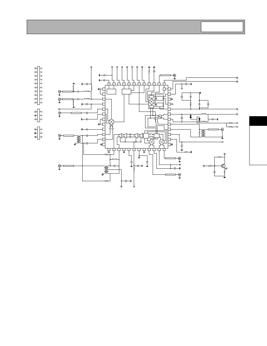
Evaluation Board Schematic
Dual Output Band
Band Gap
Rel
Bias
Supply
Quad
/2
48
45
46
47
44
43
42
41
40
39
38
37
13
16
15
14
17
18
19
20
21
22
23
24
1
2
3
4
5
6
7
8
9
10
11
12
36
35
34
33
32
31
30
29
28
27
26
25
L1
100 nH
C3
0.5 pF
50
�
strip
J1
PCS
RF OUT
VCC
C18
10 nF
VCC
C5
100 pF
50
�
strip
J2
LO2
C6
100 pF
C9
1 nF
T1
T4-1
50
�
strip
J3
MIX IN
C8
1 nF
C7
1 nF
C1
1 nF
C2
10 nF
VCC MODE CE
TX
EN
MIX
EN
VCO
EN
PLL
ON
R3
270
C19
1 nF
50
�
strip
J8
OSC REF
SET1
SET2
R2
47 k
C13
10 nF
VCC
T3
T4-1
R7
200
50
�
strip
J7
L01
D1
L2
39 nH
C16*
L3
39 nH
VCC
R8*
C17
10 nF
R9
3.9 k
VTUNE
DO
LD
C20
10 nF
DO
T2
T4-1
50
�
strip
J4
MOD OUT
C10
10 nF
VCC
C11
1 nF
C12
1 nF
R1
39 k
VGC
VCC
C23
10 nF
50
�
strip
J5
OSIG
C24
10 nF
REF
50
�
strip
J6
ISIG
P1
1
2
3
4
5
6
7
8
9
10
LDOUT
GND
SET2
SET1
PLLON
VCO EN
MIX EN
TX EN
CE
MODE
P2
1
2
3
VGC
GND
REF
P3
1
2
3
VCC
GND
VTUNE
Lock
Detect
/R
/N
Charge
Pump
R4
36 k
C26
1 nF
C22
220 pF
C21
2.2 nF
C27
33 pF
2668401-
C4
10 nF
Chip Enable
R5
510
LD
C25
10 nF
R10
510 k
R6*
LD OUT
Q1
PNP
Digikey
MMBT3906DICT-ND
VCC
L4*
22 nH
R11*
C28*
4 pF
R12*
L5
10 nH
L6*
C29
3 pF
L7
22 nH
L8*
50
�
strip
J9
Cellular
RF OUT
*Denotes not normally populated.
Preliminary
5-84
RF2668
Rev B4 010423
5
MO
D
U
LA
T
O
R
S
A
N
D
UP
C
O
N
V
E
R
T
E
RS
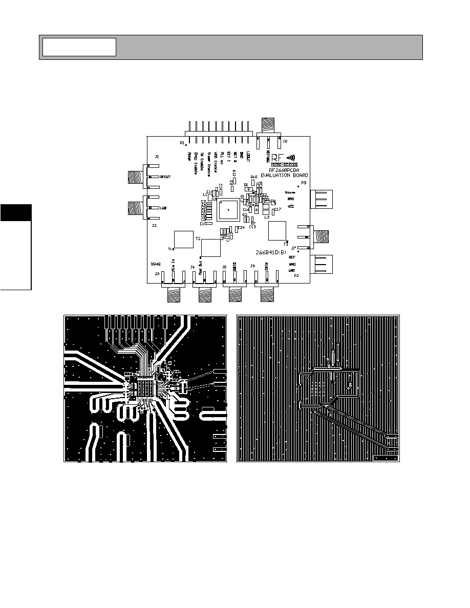
Evaluation Board Layout
2.500" X 2.250"
Board Thickness 0.031", Board Material FR-4
Preliminary
5-85
RF2668
Rev B4 010423
5
MO
D
U
LA
T
O
R
S
A
N
D
UP
C
O
N
V
E
R
T
E
RS
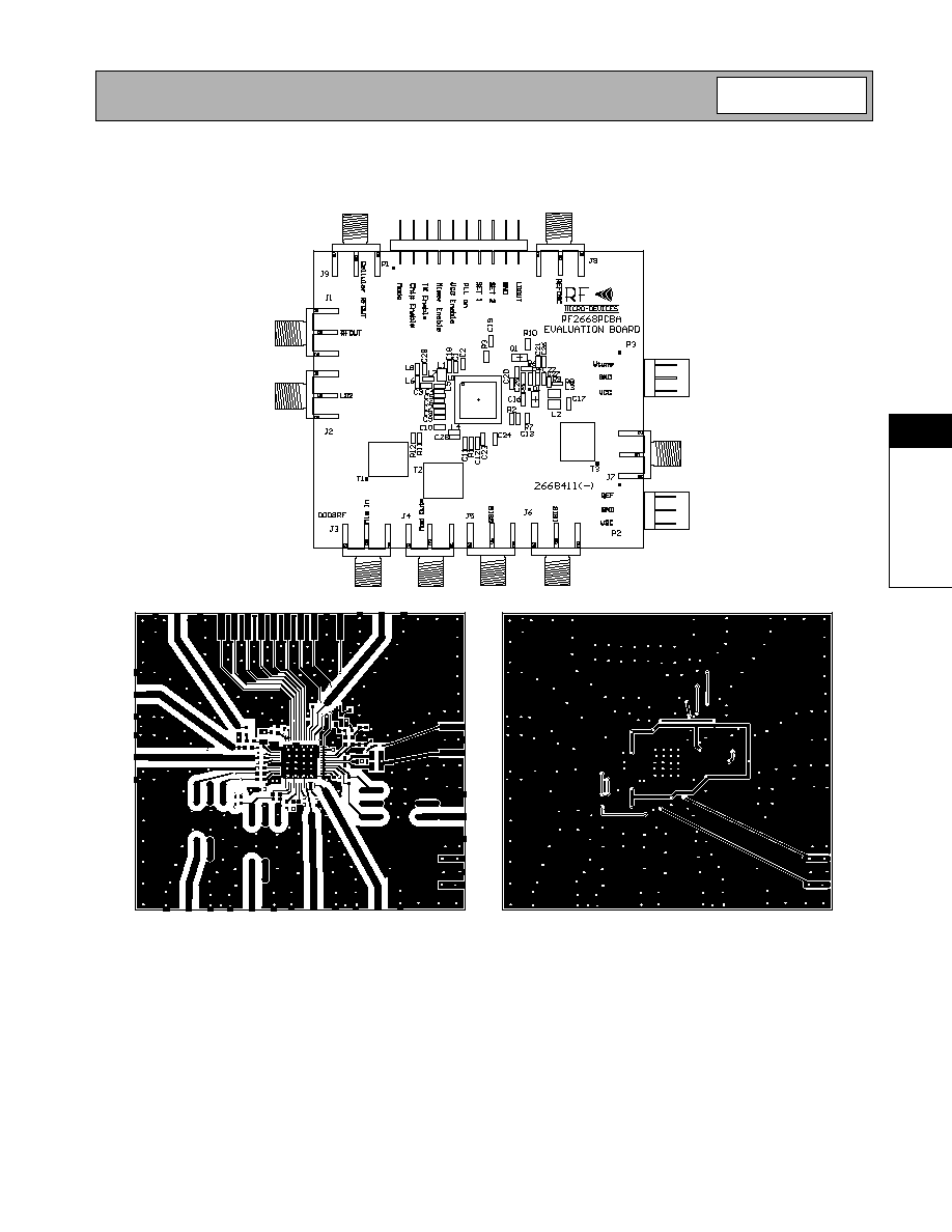
Evaluation Board Layout - Dual Band Output

Preliminary
5-86
RF2668
Rev B4 010423
5
MO
D
U
LA
T
O
R
S
A
N
D
UP
C
O
N
V
E
R
T
E
RS