 | –≠–Ľ–Ķ–ļ—ā—Ä–ĺ–Ĺ–Ĺ—č–Ļ –ļ–ĺ–ľ–Ņ–ĺ–Ĺ–Ķ–Ĺ—ā: RF2670 | –°–ļ–į—á–į—ā—Ć:  PDF PDF  ZIP ZIP |

10-45
10
IF
AMP
L
IE
R
S
Product Description
Ordering Information
Typical Applications
Features
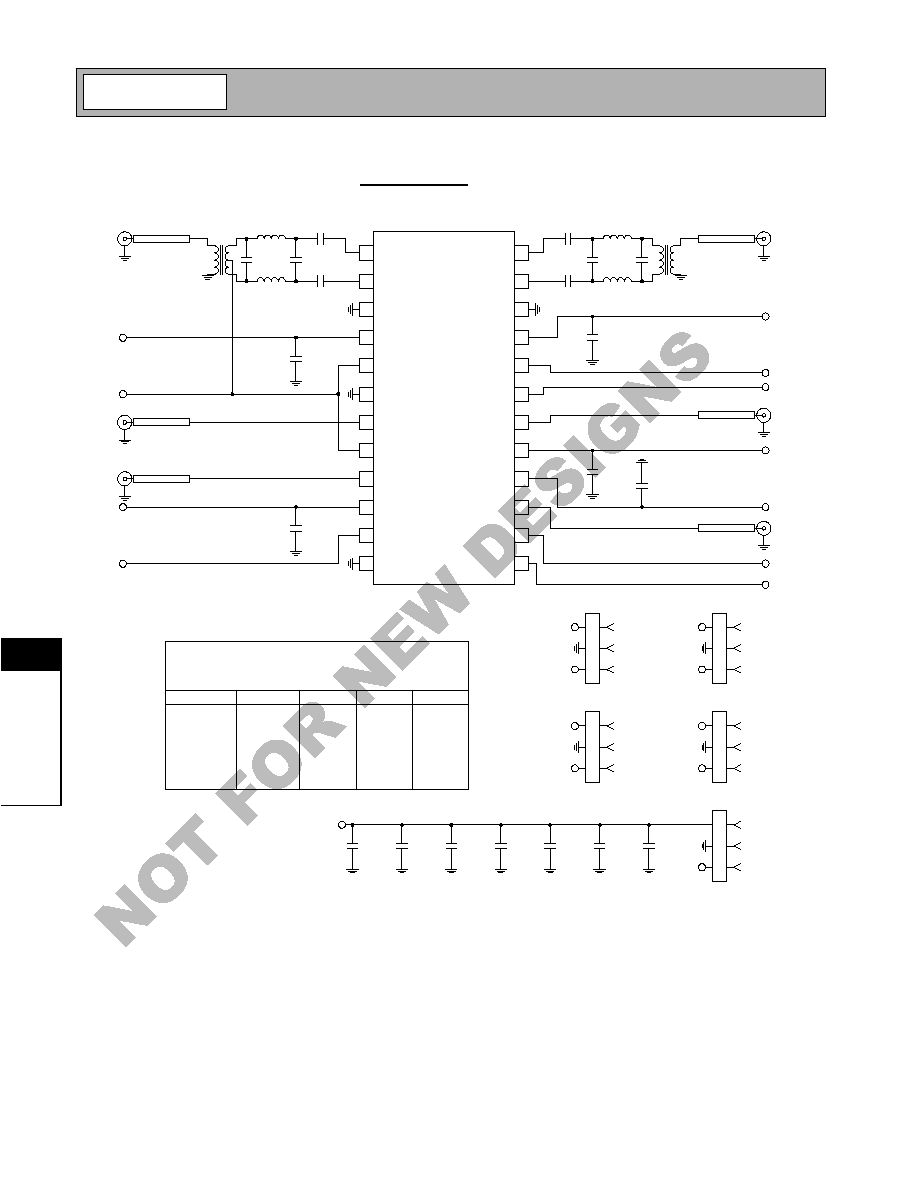
Functional Block Diagram
RF Micro Devices, Inc.
7625 Thorndike Road
Greensboro, NC 27409, USA
Tel (336) 664 1233
Fax (336) 664 0454
http://www.rfmd.com
Optimum Technology Matchingģ Applied
Si BJT
GaAs MESFET
GaAs HBT
Si Bi-CMOS
Ł
SiGe HBT
Si CMOS
0-25 dB
0-20 dB
-12-+12
17dB
6 dB
PD
BW SEL2
BW SEL1
RSSI Q
RSSI I
VREF
IN I+
IN I-
DCFB I
V
CC2
DCFB Q
IF OUT Q
Q DATA
V
CC3
V
CC1
IN Q+
IN Q-
IF OUT I
I DATA
1
2
11
14
13
24
23
20
19
5
8
15
18
21
10
17
16
9
7
4
VGC
DC
Bias
RF2670
8MHZ DUAL BASEBAND AGC WITH
PROGRAMMABLE LOW PASS FILTERING
∑ Digital Cordless Telephones
∑ Secure Communication Links
∑ Wireless LANs
∑ Inventory Tracking
∑ Wireless Security
∑ Battery Powered Applications
The RF2670 is a monolithic integrated circuit specifically
designed for direct conversion to baseband QPSK receiv-
ers. The part provides dual baseband amplifiers with a
70dB gain range (single pin analog input) and separate I
and Q RSSI. On-chip programmable baseband filters are
incorporated into each amplifier providing 1 MHz, 2MHz,
4 MHz, or 8MHz bandwidth with a 5-pole Bessel
response. I and Q output are available in digital or analog
form. The data comparators use a self generated DC ref-
erence to track DC offsets in the received signal. The
analog outputs have a 500 mVpp swing with approxi-
mately 1.7V DC offset. A 2.0V reference voltage is also
available for A/D converters changing DC bias.
∑ I/Q Baseband Receivers
∑ 10dB to 80dB Gain Range
∑ Digital and Analog Outputs
∑ On-Chip Selectable IF Bandwidths
∑ Reference Voltage for A/D Converter
∑ 2.7V to 3.6V Operation
RF2670
8MHz Dual Baseband AGC with Programmable Low
Pass Filtering
RF2670PCBA
Fully Assembled Eval Board.
10
Rev A4 010820
.069
.053
.050
.016
8įMAX
0įMIN
.010
.008
.157
.150
.244
.228
1
.344
.337
.012
.008
.025
.010
.004
.033
Package Style: SSOP-24

10-46
RF2670
Rev A4 010820
10
IF
AMP
L
IE
R
S
Absolute Maximum Ratings
Parameter
Ratings
Unit
Supply Voltage
-0.5 to +3.6
V
DC
Control Voltages
-0.5 to +3.6
V
DC
Input RF Level
+20
dBm
Operating Ambient Temperature
-40 to +85
įC
Storage Temperature
-40 to +150
įC
Parameter
Specification
Unit
Condition
Min.
Typ.
Max.
Baseband Amplifiers
T = 25įC, V
CC
=3.0V
Frequency Range
0.01
8
MHz
Minimum frequency is dependent upon input
blocking cap, DC feedback cap, and gain
setting. Recommended components yields a
minimum frequency of less than 10kHz.
Voltage Gain
77
80
83
dB
Noise Figure
5
dB
At maximum gain setting
35
dB
At minimum gain setting
Input IP3
-65
dBm
At maximum gain setting
+2
dBm
At minimum gain setting
Output DC offset
0
25
mV
Gain Control Range
65
70
dB
Gain Control Voltage Range
1.2
2.0
V
Gain Control Sensitivity
-0.08
dB/mV
VGA Output Voltage
500
mV
PP
VGA DC Output Voltage
1.7
V
Output P1dB
1
1.64
V
PP
Driving a 5k
load
RSSI Range
55
60
dB
At maximum gain setting
RSSI Output Voltage Compli-
ance
0.5 to 2.4
V
Maximum RSSI is 2.5V or V
CC
-0.3, which-
ever is less.
Input Impedance
1.5
2
2.5
k
Differential
Integrated Filters
Characteristics
Five pole Bessel
Five pole Bessel internal LPF.
Three pole external LPF.
Bandwidth
1, 2, 4, 8
MHz
Selectable from 1MHz, 2MHz, 4MHz, and
8MHz.
Passband Ripple
1
dB
Group Delay
100
ns
At 8MHz, increasing as bandwidth
decreases.
Ultimate Rejection
50
80
dB
Data Amplifiers
Voltage Gain
100
dB
Bandwidth
8
MHz
Rise and Fall Time
2
5
ns
5pF Load
Logic High Output
V
CC
-0.3V
V
Can sink/source 1mA and maintain these
logic levels.
Logic Low Output
0.3
V
Can sink/source 1mA and maintain these
logic levels.
Hysteresis
40
mV
Power Down Control
Logical Controls "ON"
V
CC
-0.3V
V
Voltage supplied to the input
Logical Controls "OFF"
0.3
V
Voltage supplied to the input
Control Input Impedance
>1
M
Turn on Time
10
13
ms
With recommended DC feedback cap
(270nF)
Caution! ESD sensitive device.
RF Micro Devices believes the furnished information is correct and accurate
at the time of this printing. However, RF Micro Devices reserves the right to
make changes to its products without notice. RF Micro Devices does not
assume responsibility for the use of the described product(s).

10-47
RF2670
Rev A4 010820
10
IF
AMP
L
IE
R
S
Parameter
Specification
Unit
Condition
Min.
Typ.
Max.
Power Supply
Voltage
2.7
3.0
3.6
V
Current Consumption
13
17
mA
V
CC
= 3.0V; PD= High
1
Ķ
A
V
CC
= 3.0V; Sleep Mode, PD= Low

10-48
RF2670
Rev A4 010820
10
IF
AMP
L
IE
R
S
Pin
Function
Description
Interface Schematic
1
IN I-
Complementary input for the in-phase IF channel.
2
IN I+
Input for the in-phase IF channel.
3
GND2
Ground for VCC2.
4
DCFB I
DC feedback capacitor for in-phase channel.
5
VCC2
Power supply for VGA amplifier 3, differential to single-ended converter,
and post filter.
6
GND3
Ground for VCC3.
7
IF OUT I
Analog signal IF output for in-phase channel.
8
VCC3
Power supply for data amplifier.
9
I DATA
Logic-level data output for the in-phase channel. This is a digital output
signal obtained from the output of a Schmitt trigger.
10
RSSI I
Received signal strength indicator for the in-phase channel.
11
PD
Enable pin for the receiver circuits. PD >2.0V powers up all of the func-
tions. PD< 1.0V turns off all of the functions.
12
GND1
Ground for VCC1 for both the in-phase and quadrature channels.
13
BW SEL1
Bandwidth select logic input. Pin 13 and pin 14 provide a two bit control
word for the setting of the IF bandwidth. See Table1. Additional filtering
should be used at the amplifiers to precisely control the 3dB bandwidth
of the system. See design information details about differential input fil-
ters.
14
BW SEL2
See pin 13.
15
Q DATA
Logic-level data output for the quadrature channel. This is a digital out-
put signal obtained from the output of a Schmitt trigger.
16
RSSI Q
Received signal strength indicator for the quadrature channel.
17
VREF
Gain control reference voltage.
18
IF OUT Q
Analog signal IF output for quadrature channel.
19
VGC
Gain control voltage.
20
VCC1
Power supply for bias circuits and VGA amplifiers for both the in-phase
and quadrature channels.
21
DCFB Q
DC feedback capacitor for quadrature channel.
22
GND1
Ground for VCC1 for both the in-phase and quadrature channels.
23
IN Q+
Plus input for quadrature channel
24
IN Q-
Minus input for quadrature channel
Table 1: Bandwidth Selection Controls
BWSEL1
BWSEL2
IF
-3dB
Frequency
0
0
1MHz
0
1
2MHz
1
0
4MHz
1
1
8MHz

10-49
RF2670
Rev A4 010820
10
IF
AMP
L
IE
R
S
Differential Filter Design Information
Butterworth Response
RS
RS
C1
L
L
RL
RL
C2
C1
C1bw
1
2
--- 10
12
2
fc RL
-------------------------------------- C2
C2bw
1
2
--- 10
12
2
fc RL
-------------------------------------- L
Lbw RL 10
6
2
fc
-----------------------------------
=
;
=
;
=
C1bw
5.1672 C2bw
;
15.4554 Lbw
;
0.1377
=
=
=
RS
125 RL
;
1000
RS
RL
-------
;
0.125
=
=
=
Differential LC Filter Component Values
(Butterworth Response)
1
10
100
1000
10000
100000
1.E+05
1.E+06
1.E+07
Frequency
C
o
mponent
V
a
l
u
e
C2 (pF)
C1 (pF)
L (
Ķ
H)

10-50
RF2670
Rev A4 010820
10
IF
AMP
L
IE
R
S
Differential Filter Design Information (Cont.)
Bessel Response
RS
RS
C1
L
L
RL
RL
C2
C1
C1bw
1
2
--- 10
12
2
fc RL
-------------------------------------- C2
C2bw
1
2
--- 10
12
2
fc RL
-------------------------------------- L
Lbw RL 10
6
2
fc
-----------------------------------
=
;
=
;
=
C1bw
2.9825 C2bw
;
15.4697 Lbw
;
0.0860
=
=
=
RS
125 RL
;
1000
RS
RL
-------
;
0.125
=
=
=
Differential LC Filter Component Values
(Bessel Response)
1
10
100
1000
10000
100000
1.E+05
1.E+06
1.E+07
Frequency
C
o
mponent
V
a
l
u
e
C2 (pF)
C1 (pF)
L (
Ķ
H)

10-51
RF2670
Rev A4 010820
10
IF
AMP
L
IE
R
S
Pin Out
1
2
3
4
5
6
7
8
9
10
11
12
24
23
22
21
20
19
18
17
16
15
14
13
IN-I
IN+I
GND2
DCFBI
VCC2
GND3
IF OUT I
VCC3
I DATA
RSSI I
PD
GND1
IN-Q
IN+Q
GND1
DCFBQ
VCC1
VGC
IF OUT Q
V REF
RSSI Q
Q DATA
BW SEL2
BWSEL1
10-52
RF2670
Rev A4 010820
10
IF
AMP
L
IE
R
S
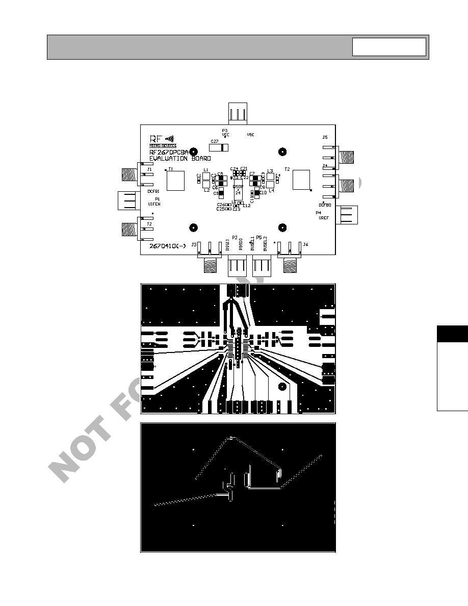
Evaluation Board Schematic
(Download Bill of Materials from www.rfmd.com.)
C26
10 nF
C25
100 pF
C24
10 nF
C23
100 pF
C22
10 nF
C21
100 pF
P3-1
1
2
3
4
5
6
7
8
9
10
11
12
24
23
22
21
20
19
18
17
16
15
14
13
IN I-
IN I+
GND2
DCFB I
VCC2
GND3
IF OUT I
VCC3
I DATA
RSSI I
V IF EN
GND1
IN Q-
IN Q+
GND1
DCFB Q
VCC1
VGC
IF OUT Q
VREF
RSSI Q
Q DATA
BW SEL2
BW SEL1
C6
100 nF
C5
100 nF
C2
1 nF
L1
10
Ķ
H
C1
220 pF
T1
50
Ķ
strip
J1
I IN
L2
10
Ķ
H
DCFB I
C9
220 nF
VCC
50
Ķ
strip
J2
IF OUT I
50
Ķ
strip
J3
I DATA
RSSI I
C13
68 pF
V IF EN
C8
100 nF
C7
100 nF
C3
1 nF
L3
10
Ķ
H
C4
220 pF
T2
50
Ķ
strip
J4
Q IN
L4
10
Ķ
H
DCFB Q
C10
220 nF
VCC
VGC
50
Ķ
strip
J5
IF OUT Q
VREF
C11
47 nF
RSSI Q
C12
68 pF
50
Ķ
strip
J6
Q DATA
BW SEL2
BW SEL1
C27
10
Ķ
F
2670400-
P5
1
2
3
P5-1
BW SEL2
GND
P5-3
BW SEL1
P4
1
2
3
P4-1
DCFB Q
GND
P4-3
VREF
P3
1
2
3
VCC
GND
P3-3
VGC
P2
1
2
3
P2-1
RSSI Q
GND
P2-3
RSSI I
P1
1
2
3
P1-1
V IF EN
GND
P1-3
DCFB I
L1-L4 and C1-C4 make two LPFs. The fc of the RF2670 is variable;
therefore the L and C components must be variable. The following
table gives recommended component values ("std" indicates standard
eval board value).
Desired BW
BW1, BW2
C1, C4 (pF) C2, C3 (pF)
L1-L4 (
Ķ
H)
700 kHz
1.4 MHz
2.8 MHz
7.0 MHz
0 0
0 1
1 0
1 1
330
220 (std)
100
33
1800
1000 (std)
470
180
22
10
4.7
2.2
10-53
RF2670
Rev A4 010820
10
IF
AMP
L
IE
R
S
Evaluation Board Layout
Board Size 3.0" x 2.0"
10-54
RF2670
Rev A4 010820
10
IF
AMP
L
IE
R
S
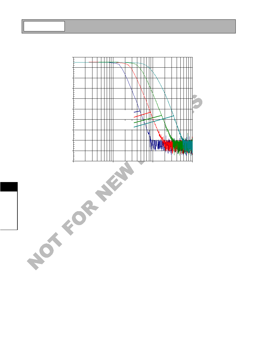
RF2670 IF Bandwidth Response
-35.0
-25.0
-15.0
-5.0
5.0
15.0
25.0
35.0
45.0
55.0
65.0
0.1
1.0
10.0
100.0
IF Frequency (MHz)
Gain
(dB)
BW_SEL (0-0)
BW_SEL (0-1)
BW_SEL (1-0)
BW_SEL (1-1)

10-55
RF2670
Rev A4 010820
10
IF
AMP
L
IE
R
S
IIP3 versus Voltage Gain
-80.0
-70.0
-60.0
-50.0
-40.0
-30.0
-20.0
-10.0
0.0
10.0
0.0
10.0
20.0
30.0
40.0
50.0
60.0
70.0
80.0
90.0
Voltage Gain (dB)
IP3
(dB)
-40įC
+25įC
+100įC
Noise Figure versus Voltage Gain
(Non-Matched Input Z)
0.0
5.0
10.0
15.0
20.0
25.0
30.0
35.0
40.0
0.0
10.0
20.0
30.0
40.0
50.0
60.0
70.0
80.0
90.0
Voltage Gain (dB)
Noise
Figure
(
dB)
-40įC
+25įC
+100įC
Voltage Gain versus Gain Control Voltage
0.0
10.0
20.0
30.0
40.0
50.0
60.0
70.0
80.0
90.0
1.2
1.3
1.4
1.5
1.6
1.7
1.8
1.9
2
Gain Control Voltage (V)
Voltage
Gain
(dB)
-40įC
+25įC
+100įC

10-56
RF2670
Rev A4 010820
10
IF
AMP
L
IE
R
S