8-347
Product Description
Ordering Information
Typical Applications
Features
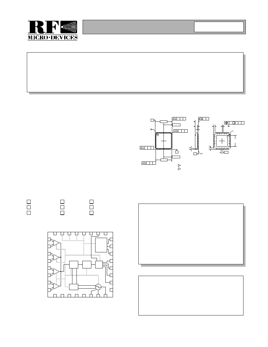
Functional Block Diagram
RF Micro Devices, Inc.
7628 Thorndike Road
Greensboro, NC 27409, USA
Tel (336) 664 1233
Fax (336) 664 0454
http://www.rfmd.com
Optimum Technology MatchingÆ Applied
Si BJT
GaAs MESFET
GaAs HBT
Si Bi-CMOS
SiGe HBT
Si CMOS
InGaP/HBT
GaN HEMT
SiGe Bi-CMOS
DI
G
V
C
C
GPO1
LN
A VCC
LNA 2P
LNA 2N
LNA 3P
LNA 3N
LNA 4P
LNA 4N
MI
X VC
C
GN
D
LO VC
C1
VCO OUT
VT
VT
C
FLT VCC
VCO V
C
C
QB OUT
Q OUT
SSB
IB OUT
SCK
SDI
CL
K
I
N
RX
E
N
GPO2
GPO3
GPO4
LO VC
C2
I OUT
LNA 1P
LNA 1N
LNA3
LNA4
DC
Correct
Quadrature
Generator
9
10
11
12
13
14
15
16
24
23
22
21
20
19
18
17
25
26
27
28
29
30
31
32
1
2
3
4
5
6
7
8
LNA1
LNA2
Polyphase
Filter
Quadrature
Mixer
Serial
Data
Interface
RF2710
VERY LOW IF RECEIVER
FOR GSM/GPRS/EDGE
∑ EGSM/DCS Handsets
∑ EGSM/DCS/PCS Handsets
∑ GSM850/PCS Handsets
∑ GSM850/EGSM/DCS/PCS Handsets
The RF2710 is a highly-integrated receiver IC supporting
GSM, GPRS, and EDGE cellular standards in the
GSM850, EGSM, DCS, and PCS bands. The RF2710,
RF6001 (synthesizer/digital filter) and RF3140 PA module
constitute RFMD's low-cost GSM transceiver solution.
RF2710 employs very-low intermediate frequency (VLIF)
receiver architecture, reducing external component count
and eliminating the need for IF SAW and RF interstage fil-
ters without compromising performance. The IC includes:
four LNA's for multi-band support; an integrated voltage
controlled oscillator (VCO); automatic gain control (AGC);
and, a quadrature downconverting mixer. Active band-
pass filters at the VLIF provide image and interference
rejection. Chip functionality, including IF AGC setting, is
controlled through a three-wire serial data interface (SDI).
∑ GSM850, EGSM, PCS & DCS Operation
∑ Very-Low IF Architecture Eliminates
IFSAW and RF Interstage Filters
∑ Integrated RF VCO
∑ Integrated LNA's support up to four RF
bands
RF2710
Very Low IF Receiver for GSM/GPRS/EDGE
RF2710 PCBA
Fully Assembled Evaluation Board
0
Rev A0 030130
2 PLCS
0.15 C
B
-B-
4.75 SQ.
2.50 TYP.
2.37 TYP.
5.00 SQ.
2 PLCS
0.15 C
A
-A-
3
2 PLCS
0.15 C
B
2 PLCS
0.15 C
A
0.05
0.00
0.70
0.65
0.90
0.85
0.05 C
12∞
MAX
-C-
SEATING
PLANE
0.50
3.45
3.15
SQ.
Pin 1 ID
R.20
0.50
0.30
2
C
A
B
0.10 M
0.30
0.18
0.60
0.24
TYP.
NOTES:
1. Shaded pin is lead 1.
3. Pin 1 identifier must exist on top surface of package between identification mark or feature
on the package body. Exact shape and size are optional.
3
2. Dimension applies to plated terminal: to be measured between 0.20 mm and 0.25 mm
from terminal end.
2
4. Package warpage: max. 0.05 mm.
5. Die thickness allowable: 0.305 mm max.
Package Style: QFN, 32-Pin, 5x5
Preliminary
!