7-17
5
MO
D
U
LA
T
O
R
S
A
N
D
UP
C
O
N
V
E
R
T
E
RS
Preliminary
Product Description
Ordering Information
Typical Applications
Features
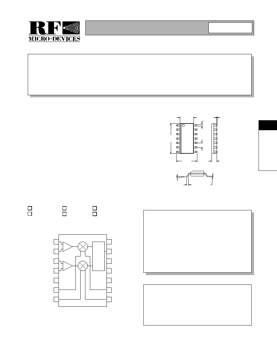
Functional Block Diagram
RF Micro Devices, Inc.
7625 Thorndike Road
Greensboro, NC 27409, USA
Tel (336) 664 1233
Fax (336) 664 0454
http://www.rfmd.com
Optimum Technology Matching� Applied
Si BJT
GaAs MESFET
GaAs HBT
Si Bi-CMOS
�
SiGe HBT
Si CMOS
1
2
3
4
5
6
7
14
13
12
11
10
9
8
I INPUT A
I INPUT B
Q INPUT A
Q INPUT B
BG OUT
I IF OUT
Q IF OUT
VCC
LO INPUT
GND
GND
GND
I OUT
Q OUT
QUAD
DIV.
BY 2
RF2713
QUADRATURE MODULATOR/DEMODULATOR
� Digital and Analog Receivers and
Transmitters
� High Data Rate Digital Communications
� Spread-Spectrum Communication Systems
� Interactive Cable Systems
� Portable Battery-Powered Equipment
The RF2713 is a monolithic integrated quadrature modu-
lator/demodulator. The demodulator is used to recover
the I and Q baseband signals from the amplified and fil-
tered IF. Likewise, the inputs and outputs can be reconfig-
ured to modulate I/Q signals onto an RF carrier. The
RF2713 is intended for IF systems where the IF fre-
quency ranges from 100kHz to 250MHz, and the LO fre-
quency is two times the IF. The IC contains all of the
required components to implement the modulation/
demodulation function and contains a digital divider type
90� phase shifter, two double balanced mixers, and base-
band amplifiers designed to interface with Analog to Digi-
tal Converters. The unit operates from a single 3V to 6V
power supply.
� 3V to 6V Operation
� Modulation or Demodulation
� IF From 100kHz to 250MHz
� Baseband From DC to 50MHz
� Digital LO Quadrature Divider
� Low Power and Small Size
RF2713
Quadrature Modulator/Demodulator
RF2713 PCBA-D Fully Assembled Evaluation Board (Demodulator)
RF2713 PCBA-M Fully Assembled Evaluation Board (Modulator)
7
Rev A2 010129
0.157
0.150
0.068
0.053
0.244
0.229
0.008
0.004
0.018
0.014
8� MAX
0� MIN
0.034
0.016
0.009
0.007
0.337
0.334
0.050
Package Style: SOIC-14

Preliminary
7-18
RF2713
Rev A2 010129
5
MO
D
U
LA
T
O
R
S
A
N
D
UP
C
O
N
V
E
R
T
E
RS
Absolute Maximum Ratings
Parameter
Rating
Unit
Supply Voltage
-0.5 to 7.0
V
DC
IF Input Level
500
mV
PP
Operating Ambient Temperature
-40 to +85
�C
Storage Temperature
-40 to +150
�C
Parameter
Specification
Unit
Condition
Min.
Typ.
Max.
Overall
T = 25�C, V
CC
=3.0V, IF = 100MHz,
LO= 200MHz, F
MOD
= 500kHz
IF Frequency Range
0.1 to 250
MHz
For IF frequencies below ~2.5MHz, the LO
should be a square wave. IF frequencies
lower than 100kHz are attainable if the LO is
a square wave and sufficiently large DC
blocking capacitors are used.
Baseband Frequency Range
DC to 50
MHz
Input Impedance
1200 || 1pF
Each input, single-ended
LO
Frequency
Twice (2x) the IF frequency. For IF frequen-
cies below ~2.5MHz, the LO should be a
square wave. IF frequencies lower than
100kHz are attainable if the LO is a square
wave and sufficiently large DC blocking
capacitors are used.
Level
0.06 to 1
V
PP
Input Impedance
500 || 1pF
Demodulator
Configuration
IF
IN
=28mV
PP
, LO= 200mV
PP
, Z
LOAD
=10k
Output Impedance
50 || 1pF
Each output, I
OUT
and Q
OUT
Maximum Output
1.4
V
PP
Saturated
Voltage Gain
20
dB
V
CC
= 3.0V
22.5
24
25.1
dB
V
CC
= 5.0V
Noise Figure
24
dB
Single Sideband, IF Input of device reac-
tively matched
35
dB
Single Sideband, 50
shunt resistor at IF
Input
Input Third Order Intercept Point
(IIP
3
)
-22
dBm
V
CC
= 3.0V, IF Input of device reactively
matched
-11
dBm
V
CC
= 3.0V, 50
shunt resistor at IF Input
-19
V
CC
= 5.0V, IF Input of device reactively
matched
-8
dBm
V
CC
= 5.0V, 50
shunt resistor at IF Input
-28
dBm
V
CC
= 5.0V, IF Input of device reactively
matched, Z
LOAD
= 50
I/Q Amplitude Balance
0.1
0.5
dB
Quadrature Phase Error
1
�
DC Output
800
mV
V
CC
= 3.0V, I
OUT
and Q
OUT
to GND
2.0
2.4
2.8
V
V
CC
= 5.0V, I
OUT
and Q
OUT
to GND
DC Offset
<10
100
mV
I
OUT
to Q
OUT
Caution! ESD sensitive device.
RF Micro Devices believes the furnished information is correct and accurate
at the time of this printing. However, RF Micro Devices reserves the right to
make changes to its products without notice. RF Micro Devices does not
assume responsibility for the use of the described product(s).

Preliminary
7-19
RF2713
Rev A2 010129
5
MO
D
U
LA
T
O
R
S
A
N
D
UP
C
O
N
V
E
R
T
E
RS
Parameter
Specification
Unit
Condition
Min.
Typ.
Max.
Modulator Configuration
IF
IN
=28mV
PP
, LO= 200mV
PP
,
Z
LOAD
= 1200
Maximum Output
200
mV
PP
Saturated
Input Voltage
90
mV
PP
Single Sideband, 1dB Gain Compression.
Voltage Gain
6
dB
Single Sideband
I/Q Amplitude Balance
0.1
dB
Quadrature Phase Error
<�1
�
Carrier Suppression
25
dBc
Unadjusted. Carrier Suppression may be
optimized further by adjusting the DC offset
level between the A and B inputs.
Sideband Suppression
30
dBc
Power Supply
Voltage
2.7 to 6
V
Operating limits
Current
8
mA
V
CC
= 3.0V
8
10
12
mA
V
CC
= 5.0V
Preliminary
7-20
RF2713
Rev A2 010129
5
MO
D
U
LA
T
O
R
S
A
N
D
UP
C
O
N
V
E
R
T
E
RS
Pin
Function
Description (Demodulator Configuration)
Interface Schematic
1
I INPUT A
When the RF2713 is configured as a Quadrature Demodulator, both
mixers are driven by the IF. Whether driving the mixers single-endedly
(as shown in the application schematic) or differentially, the A Inputs
(pins 1 and 3) should be connected to each other. Likewise, both B
Inputs (pins 2 and 4) should be connected to each other. This ensures
that the IF will reach each mixer with the same amplitude and phase,
yielding the best I and Q output amplitude and quadrature balance.
Note that connecting the inputs in parallel changes the input imped-
ance (see the Gilbert Cell mixer equivalent circuit). The single-ended
input impedance (as shown in the application circuit) becomes 630
,
but in the balanced configuration, the input impedance would remain
1260
.
The mixers are Gilbert Cell designs with balanced inputs. The equiva-
lent schematic for one of the mixers is shown on the following page.
The input impedance of each pin is determined by the 1260
resistor
to V
CC
in parallel with a transistor base. Note from the schematic that
all four input pins have an internally set DC bias. For this reason, all
four inputs (pins 1 through 4) should be DC blocked. The capacitance
values of the blocking capacitors is determined by the IF frequency.
When driving single-endedly, both the series (pins 1 and 3) and shunt
(pins 2 and 4) blocking capacitors should be low impedances, relative
to the 630
input impedance.
2
I INPUT B
Same as pin 1, except complementary input.
See pin 1.
3
Q INPUT A
Same as pin 1, except Q Buffer Amplifier.
See pin 1.
4
Q INPUT B
Same as pin 3, except complementary input.
See pin 1.
5
BG OUT
Band Gap voltage reference output. This voltage output is held con-
stant over variations in supply voltage and operating temperature and
may be used as a reference for other external circuitry. This pin should
not be loaded such that the sourced current exceeds 1mA. This pin
should be bypassed with a large (0.1
�
F) capacitor.
6
I IF OUT
This pin is not used in the Demodulator Configuration, but must be con-
nected to V
CC
in order to properly bias the I mixer.
7
Q IF OUT
Same as pin 6, except Q mixer.
Same as pin 6.
8
Q OUT
Q Mixer's Baseband Output. This pin is NOT internally DC blocked and
has DC present due to internal biasing. This is an emitter-follower type
output with an internal 2k
pull-down resistor. Even though the AC out-
put impedance is ~50
, this pin is intended to drive only high imped-
ance loads such as an opamp or an ADC. The output transistor is NOT
biased such that it can drive a large signal into a 50
load. DC cou-
pling of this output is permitted provided that the DC impedance to
ground, which appears in parallel with the internal pull-down resistor, is
significantly greater than 2k
.
9
I OUT
Same as pin 8, except Q Mixer's Baseband Output.
Same as pin 8.
10
GND
Ground connection. Keep traces physically short and connect immedi-
ately to ground plane for best performance.
11
GND
Same as pin 10.
12
GND
Same as pin 10.
1260
1260
INPUT A
V
CC
V
CC
INPUT B
IF OUT
I/Q OUT
2 k
V
CC

Preliminary
7-21
RF2713
Rev A2 010129
5
MO
D
U
LA
T
O
R
S
A
N
D
UP
C
O
N
V
E
R
T
E
RS
Pin
Function
Description (Demodulator Configuration)
Interface Schematic
13
LO INPUT
High impedance, single-ended modulator LO input. The LO applied to
this pin is frequency divided by a factor of 2 and becomes the "Carrier".
For direct demodulation, the Carrier is equal in frequency to the center
of the input IF spectrum (except in the case of SSB/SC). The input
impedance is determined by an internal 500
bias resistor to V
CC
. An
external blocking capacitor should be provided if the pin is connected to
a device with DC present. Matching the input impedance is typically
achieved by adding a 51
resistor to ground on the source side of the
AC coupling capacitor. For the LO input, maximum power transfer is not
critical. The internal LO switching circuits are controlled by the voltage,
not power, into the part. In cases where the LO source does not have
enough available voltage, a reactive match (voltage transformer) can
be used. The LO circuitry consists of a limiting amplifier followed by a
digital divider. The limiting amp ensures that the flip-flop type divider is
driven with a square wave over a wide range of input levels. Because
the flip-flop uses the rising and falling edges of the limiter output, the
quadrature accuracy of the Carrier supplied to the mixers is directly
related to the duty cycle, or equivalently to the even harmonic content,
of the input LO signal. In particular, care should be taken to ensure that
the 2xLO level input to this pin is at least 20dB below the LO level. Oth-
erwise, the LO input is not sensitive to the type of input wave form,
except for IF frequencies below ~2.5MHz, in which case the LO input
should be a square wave, in order to ensure proper triggering of the
flip-flops. IF frequencies below 100kHz are attainable if the LO is a
square wave and sufficiently large DC blocking capacitors are used.
14
VCC
Voltage supply for the entire device. This pin should be well bypassed
at all frequencies (IF, LO, Carrier, Baseband) that are present in the
part.
500
500
LO IN
V
CC
V
CC