 | –≠–ª–µ–∫—Ç—Ä–æ–Ω–Ω—ã–π –∫–æ–º–ø–æ–Ω–µ–Ω—Ç: RF2860 | –°–∫–∞—á–∞—Ç—å:  PDF PDF  ZIP ZIP |
8-383
Product Description
Ordering Information
Typical Applications
Features
Functional Block Diagram
RF Micro Devices, Inc.
7628 Thorndike Road
Greensboro, NC 27409, USA
Tel (336) 664 1233
Fax (336) 664 0454
http://www.rfmd.com
Optimum Technology MatchingÆ Applied
Si BJT
GaAs MESFET
GaAs HBT
Si Bi-CMOS
SiGe HBT
Si CMOS
InGaP/HBT
GaN HEMT
SiGe Bi-CMOS
IF OUT+
IF OUT-
GND
LO IN
LNA GAIN
LNA IN
GND
LNA OUT
ISET2
ISET1
MIX IN
RF
VCC
16
15
14
13
11
12
9
10
5
6
7
8
2
1
4
3
VC
C
LO O
U
T
TX BUFF
EN
AB
EN
ABLE
RF2860
PCS CDMA LOW NOISE AMPLIFIER/MIXER
BROADBAND DOWNCONVERTER
∑ CDMA Korean PCS Systems
∑ CDMA US PCS Systems
∑ IMT-2000 and 2.4GHz Band Applications
∑ GPS Applications
∑ General Purpose Downconverter
∑ Commercial and Consumer Systems
The RF2860 is a broadband receiver front-end designed
for CDMA PCS applications. The broadband design
makes it a great solution as well for GPS, IMT-2000 and
2.4GHz applications. It is designed to amplify and down-
convert RF signals, while providing 21.5dB of stepped
gain control range. Features include digital control of LNA
gain, TX buffer/enable, and power down mode. Another
feature of the chip is the ability to set the bias point and
RF performance of the LNA and mixer through the ISET1
and ISET2 resistors respectively. Noise figure, IIP3, and
gain are designed to exceed the IS-98 interim standard
requirement for CDMA PCS communications. The IC is
manufactured on an advanced Silicon Germanium
Bi-CMOS process and is in a 3mmx3mm, 16-pin, lead-
less chip carrier.
∑ LNA Noise Figure=1.3dB (KPCS)
∑ Stepped LNA Gain Control
∑ Integrated TX LO Buffer Amplifier
∑ Adjustable IIP3 versus Current for both
LNA and Mixer Blocks
∑ All Pins ESD Protected
RF2860
PCS CDMA Low Noise Amplifier/Mixer Broadband
Downconverter
RF2860 PCBA Fully Assembled Evaluation Board
0
Rev A7 031105
0.90
0.85
0.05 C
0.05
0.00
0.70
0.65
12∞
MAX
-C-
SEATING
PLANE
1.50 TYP
0.10 C A
2 PLCS
-A-
3.00
0.10 C B
2 PLCS
1.37 TYP
0.10 C A
2 PLCS
2.75 SQ
0.10 C B
2 PLCS
3.00
-B-
0.60
0.24
TYP
0.50
0.30
PIN 1 ID
R.20
0.50
1.65
1.35
SQ.
0.10
C A B
M
0.30
0.18
2
NOTES:
1. Shaded lead is pin 1.
Dimension applies to plated terminal: to be measured
between 0.20 mm and 0.25 mm from terminal end.
2
Dimensions in mm.
Package Style: QFN, 16-Pin, 3x3

8-384
RF2860
Rev A7 031105
Absolute Maximum Ratings
Parameter
Rating
Unit
Supply Voltage
-0.5 to +5.0
V
DC
Input LO and RF Levels
+6
dBm
Operating Ambient Temperature
-40 to +85
∞C
Storage Temperature
-40 to +150
∞C
Parameter
Specification
Unit
Condition
Min.
Typ.
Max.
Overall
T = 25∞C, V
CC
=2.75V
RF Frequency Range
1575 to 2170
MHz
IF Frequency Range
0.1
400
MHz
Power Supply
Supply Voltage
2.65
2.75
3.15
V
Logic High
1.8
V
Logic Low
0.4
V
Power Down Current
10
µ
A
ENABLE=0
US PCS Band
Korean PCS Band
GPS Band
IMT-2000 Band
Freq=1930MHz to 1990MHz
Freq=1840MHz to 1870MHz
Freq=1575.42MHz
Freq=2110MHz to 2170MHz
LNA (On) - KPCS
LNA 50
match
Gain
14.0
16.5
17.5
dB
Noise Figure
1.3
1.5
dB
Input IP3
+6.0
+8.0
dBm
Current
6.5
mA
Isolation
20
dB
LNA (On) - US PCS
LNA 50
match
Gain
13.5
16.0
17.0
dB
Noise Figure
1.4
1.6
dB
Input IP3
+6.0
+8.0
dBm
Current
6.5
mA
Isolation
30
dB
LNA (On) - GPS Band
LNA 50
match
Gain
14.75
17.25
18.25
dB
Noise Figure
1.2
dB
Input IP3
+5.0
dBm
Current
6.0
mA
Isolation
20
dB
LNA (On) - IMT-2000 Band
LNA 50
match
Gain
12.0
14.5
15.5
dB
Noise Figure
1.4
dB
Input IP3
+8.0
dBm
Current
6.0
mA
Isolation
20
dB
LNA (Off) - US PCS, KPCS,
GPS, IMT-2000
Gain
-6.5
-5.0
-3.5
dB
Noise Figure
5.0
6.0
dB
Input IP3
+20.0
+25.0
dBm
Current
0
mA
Isolation
4
dB
Caution! ESD sensitive device.
RF Micro Devices believes the furnished information is correct and accurate
at the time of this printing. However, RF Micro Devices reserves the right to
make changes to its products without notice. RF Micro Devices does not
assume responsibility for the use of the described product(s).
8-385
RF2860
Rev A7 031105
Parameter
Specification
Unit
Condition
Min.
Typ.
Max.
US PCS Band,
Korean PCS Band,
GPS Band, IMT-2000 Band,
cont'd
Mixer - KPCS/US PCS
See note.
Gain
12.0
14.0
15.5
dB
Noise Figure
7.0
8.0
dB
Input IP3
+1.0
+3.0
dBm
Current
17.5
mA
LO to RF Isolation
36
dB
Mixer - GPS
Gain
16.5
18.5
20.0
dB
Noise Figure
7.5
dB
Input IP3
-2.0
dBm
Current
16.0
mA
LO to RF Isolation
36
dB
Mixer - IMT-2000
Gain
11.5
13.5
15.0
dB
Noise Figure
8.5
dB
Input IP3
0.0
dBm
Current
16.0
mA
LO to RF Isolation
36
dB
Other
LO-IF Isolation
36
dB
RF-IF Isolation
40
dB
LNA Out to Mixer In Isolation
30
40
dB
LO-LNA In Isolation, Any State
35
dB
Control Lines
Input Capacitance
1
pF
LNA GAIN, ENABLE, TX BUFF ENAB
Local Oscillator Input
KPCS, US PCS, GPS, IMT-2000
Input Power
-10
-4
0
dBm
Input Frequency
1391
2360
MHz
IF=183.6MHz/210.38MHz/220.38MHz
TX (Local Oscillator)
Buffer
PCS
Output Power
-11
-7
dBm
Single-ended 50
load
Output Frequency
1600
2300
MHz
Current Consumption
2
mA
NOTE: Mixer performance can be changed with external IF load/tuning.

8-386
RF2860
Rev A7 031105
LNA Performance versus Current (As a function of ISET1 Resistance)
Mixer Performance versus Current (As a function of ISET2 Resistance)
Evaluation Board Current Measurement
Cascaded Performance (Typical Values for V
CC
=2.75V)
NOTE: All total current numbers include bias circuitry current of 1.5mA to 2.0mA (dependent on mode).
Gain (dB)
IIP3 (dBm)
Noise Figure (dB)
ISET1 Resistance (k
)
Current (mA)
15.6
7.3
1.4
36
4.6
15.7
9.7
1.4
33
4.9
15.9
16.8
1.4
30
5.4
16.1
12.3
1.4
27
6.1
16.2
10.6
1.4
24
6.7
16.4
9.6
1.4
22
7.3
16.4
9.4
1.4
20
7.9
Gain (dB)
IIP3 (dBm)
Noise Figure (dB)
ISET2 Resistance (k
)
Current (mA)
14.2
4.0
6.7
6.8
25.6
14.2
3.7
6.6
7.5
24.6
14.1
3.5
6.5
8.3
23.9
14.0
2.9
6.4
9.1
22.8
13.8
2.6
6.4
10.0
22.2
13.8
2.4
6.3
11.0
21.8
13.5
1.8
6.3
12.0
20.7
ENABLE
LNA
GAIN
TX BUFF
ENAB
IDC
(mA)
US PCS Band
Korean PCS Band
LNA On, TX Buffer Off
1
1
0
27.5
LNA Bypassed, TX Buffer Off
1
0
0
21.0
GPS Band
LNA On, TX Buffer Off
1
1
0
24.5
LNA Bypassed, TX Buffer Off
1
0
0
18.5
IMT-2000 Band
LNA On, TX Buffer Off
1
1
0
24.5
LNA Bypassed, TX Buffer Off
1
0
0
18.5
NOTES:
All IDC current numbers include bias circuitry current of 1.5mA to 2.0mA
(dependent on mode).
TX Buffer On: Add 2mA to total current.
Parameter
KPCS CDMA
PCS CDMA
GPS
IMT-2000
LNA ON
LNA OFF
LNA ON
LNA OFF
LNA ON
LNA OFF
LNA ON
LNA OFF
Cascaded:
Gain (dB)
28.0
6.5
27.5
6.5
33.25
11.0
25.5
6.0
Noise Figure (dB)
1.8
14.5
2.0
14.5
1.7
15.0
2.5
16.0
Input IP3 (dBm)
-11.0
+10.0
-11.0
+10.0
-17.0
5.3
-12.0
+7.2
LO to IF Isolation (dB)
40
40
40
40
40
40
40
40
IF1 to RF Isolation (dB)
40
40
40
40
40
40
40
40
IF2 to RF Isolation (dB)
40
40
40
40
40
40
40
40
LO to LNA IN Isolation (dB)
40
40
40
40
40
40
40
40
Total Current (mA)
27.5
21.0
27.5
21.0
24.5
18.5
24.5
18.5
NOTE: Assumes 2.5dB image filter insertion loss. The TX Buffer is off.

8-387
RF2860
Rev A7 031105
Pin
Function
Type Description
Interface Schematic
1
LNA GAIN
DI
Logic input. High activates LNA. Low selects LNA bypass
mode.
2
LNA IN
AI
US PCS LNA input.
KPCS LNA input.
GPS LNA input.
IMT-2000 LNA input.
3
GND
P
Ground via within 0.2mm of pin required.
4
LNA OUT
AO
PCS LNA output. Simple external L-C components required
for matching and VCC supply.
5
ISET2
AI
External resistor required to set the mixer operating current.
6
ISET1
AI
External resistor required to set the LNA operating current.
7
MIX IN
AI
KPCS mixer RF single-end input. Matched to 50
.
USPCS mixer RF single-end input. Matched to 50
.
GPS mixer RF single-end input. Matched to 50
.
IMT-2000 mixer RF single-end input. Matched to 50
.
8
RF VCC
P
External capacitor and inductor placed close to package
required.
9
IF OUT+
AO
IF output. Open collector.
10
IF OUT-
AO
IF output. Open collector.
See pin 9.
11
GND
P
Ground.
12
LO IN
AI
LO single-end input. Matched to 50
.
13
VCC
P
External bypass capacitor may be required.
14
LO OUT
AO
LO output. Internal DC block. Drives 50
.
15
TX BUFF
ENAB
DI
Logic input. High enables TX LO output buffer amplifiers.
16
ENABLE
DI
Logic input. Low level powers down the IC.
Pkg
Base
GND
P
Ground connection. The backside of the package should be
soldered to a top side ground pad which is connected to the
ground plane with multiple vias.
Legend:
DI=Digital Input from Baseband Chip
AI=Analog Input
AO=Analog Output
P=V
CC
or GND
LNA GAIN
LNA IN
V
CC
LNA OUT
LNA EMITTER
MIX IN
IF+
IF-
LO IN
70
TX BUFF
ENAB
ENABLE

8-388
RF2860
Rev A7 031105
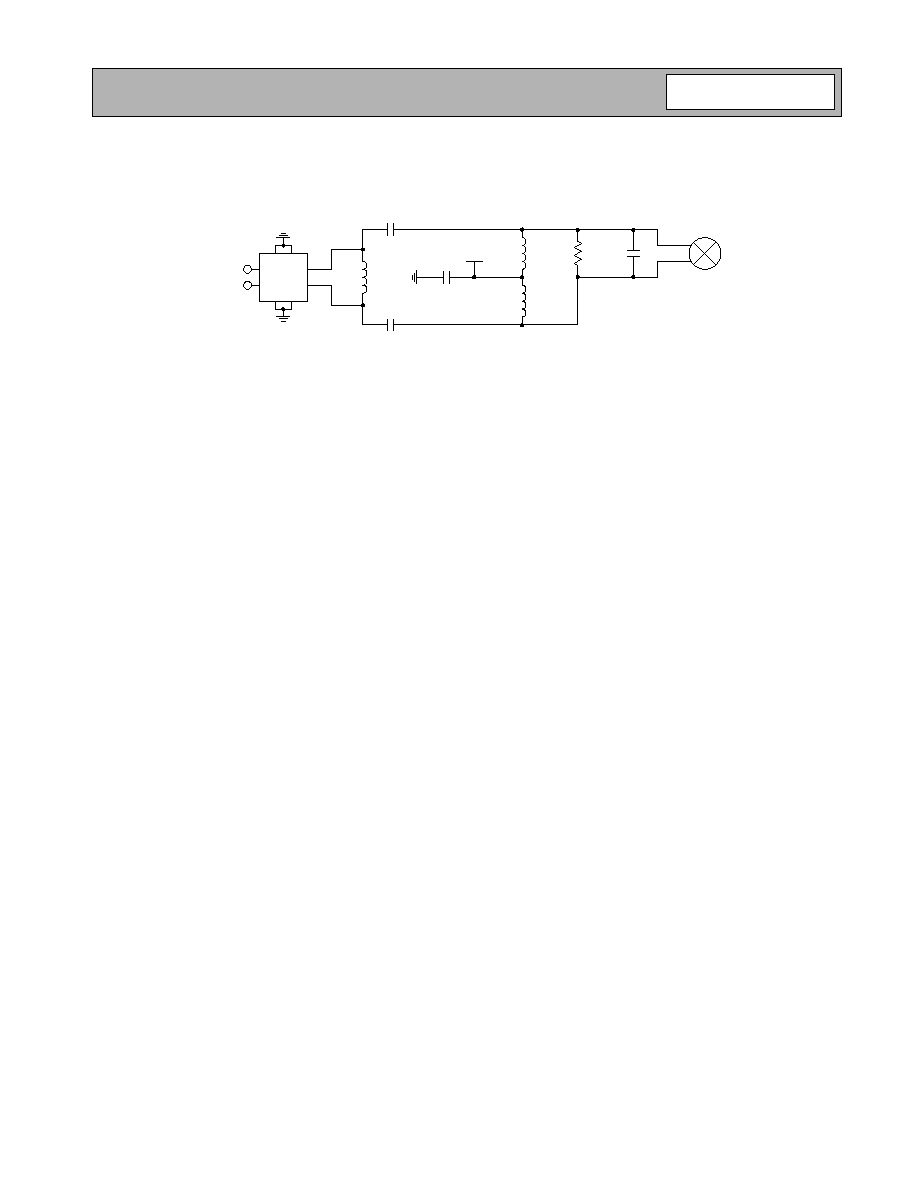
Application Schematic
Differential IF Matching
NOTES:
1. This resistor sets the LNA current. Increasing the resistor value lowers the current.
2. This resistor sets the mixer current. Increasing the resistor value lowers the current.
3. This capacitor is used for optimum noise figure and input matching.
4. This inductor is used for optimum input match.
5. This inductor is used for optimum input match and IP3. Low impedance path to ground for optimum IP3.
6. DC-blocking capacitor. Not required with most SAW filters.
7. This inductor is used for LNA output match and as an RF choke.
8. This resistor is used to optimize performance over temperature and bias.
9. This inductor is used to optimize the LNA output match.
10. This inductor/capacitor parallel combination is used for mixer/preamp interstage matching and must be placed
~1.6mm or closer to pin 8.
11. Ground for LNA. Place ground via as close to pin as possible for maximum gain.
12. IF output matching component values are dependent on board layout, IF SAW filter, and the IF frequency selected.
Please contact RFMD application engineering for assistance with IF output matching. See attached Single-Ended
and Differential Tuning procedure.
13. These two values are contingent on type of IF SAW filter used.
14. Depending on SAW Filter used, resistor value will be between 2
to 10
.
Application
C1
(pf)
C2
(pf)
C3
(pF)
C4
(pF)
L1
(nH)
L2
(nH)
L3
(nH)
L4
(nH)
L5
(nH)
L6
(nH)
L7
(nH)
R1
(k
)
R2
(k
)
R3
(k
)
US PCS,
IF=184MHz
6.2
2.5
6.2
TBD
33
72
72
TBD
15
2.7
1.2
9.1
8.2
27.0
Korean PCS,
IF=220MHz
5.1
3.0
5.1
TBD
33
50
50
TBD
15
3.3
1.5
7.5
8.2
27.0
GPS,
IF=184MHz
3.9
1.5
3.9
TBD
33
110
110
TBD
18
4.7
1.5
DNI
13.0
27.0
IMT-2000,
IF=190MHz
4.7
1.0
4.7
TBD
33
50
50
TBD
10
2.7
1.5
DNI
13.0
27.0
16
15
14
13
11
12
9
10
5
6
7
8
2
1
4
3
3 pF
R3
L5
33 nF
33 nF
LNA GAIN
ENABLE
TX BUFF ENAB
C2
L2
L1
DNI
33 nF
LNA IN
2.2 nH
LO OUT
LO IN
RF VCC
3.9 nH
L6
V
CC
V
CC
FL4
RF Saw
4
1
6
5
2
3
GND
GND
GND
GND
OU
T
I
N
L7
1 pF
30
R2
1.3 pF
R1
Note 6
Note 3
Note 4
Note 8
Note 7
Note 9
Note 14
Note 10
Note
11
Note 2
Note 1
L3
VCC
C3
C1
33 nF
33 nF
VCC
Note 12
L4
C4
FL2
IF Saw
4
5
9
10
Note 13
2 to 10
Note 5
IF OUT
8-389
RF2860
Rev A7 031105
Application Schematic
Single-End IF Matching
NOTES:
1. This resistor sets the LNA current. Increasing the resistor value lowers the current.
2. This resistor sets the mixer current. Increasing the resistor value lowers the current.
3. This capacitor is used for optimum noise figure and input matching.
4. This inductor is used for optimum input match.
5. This inductor is used for optimum input match and IP3. Low impedance path to ground for optimum IP3.
6. DC-blocking capacitor. Not required with most SAW filters.
7. This inductor is used for LNA output match and as an RF choke.
8. This resistor is used to optimize performance over temperature and bias.
9. This inductor is used to optimize the LNA output match.
10. This inductor/capacitor parallel combination is used for mixer/preamp interstage matching and must be placed
~1.6mm or closer to pin 8.
11. Ground for LNA. Place ground via as close to pin as possible for maximum gain.
12. IF output matching component values are dependent on board layout, IF SAW filter, and the IF frequency selected.
Please contact RFMD application engineering for assistance with IF output matching. See attached Single-Ended
and Differential Tuning procedure.
13. These two values are contingent on type of IF SAW filter used.
14. Depending on SAW Filter used, resistor value will be between 2
to 10
.
Application
C2
(pF)
C3
(pF)
L1
(nH)
L2
(nH)
L7
(nH)
L6
(nH)
R1
(k
)
R2
(k
)
R3
(k
)
US PCS, IF=184MHz
10.0
6.2
150
270
1.2
2.7
9.1
8.2
27.0
Korean PCS, IF=220MHz
12.0
5.1
100
180
1.5
3.3
7.5
8.2
27.0
GPS, IF=184MHz
6.0
3.9
220
270
1.5
4.7
DNI
13.0
27.0
IMT-2000, IF=190MHz
4.0
4.7
100
180
1.5
2.7
DNI
130
27.0
3 pF
R3
15 nH
33 nF
DNI
33 nF
LNA IN
LNA GAIN
ENABLE
TX BUFF ENAB
2.2 nH
LO OUT
V
CC
C2
R1
L1
L2
V
CC
33 nF
C3
CDMA IF+
CDMA IF-
LO IN
RF V
CC
3.9 nH
L6
CDMA
IF Saw
4
5
9
10
16
15
14
13
11
12
9
10
5
6
7
8
2
1
4
3
L7
1 pF
Note 5
Note 4
30
V
CC
Note 6
Note 8
R2
Note 9
Note 2
1.3 pF
Note 10
Note 7
Note 14
RF Saw
52
4
1
6
3
OU
T
IN
GND
GND
GND
GND
Note 11
33 nF
Note 3
Note 1
Note 12
2 to 10
8-390
RF2860
Rev A7 031105
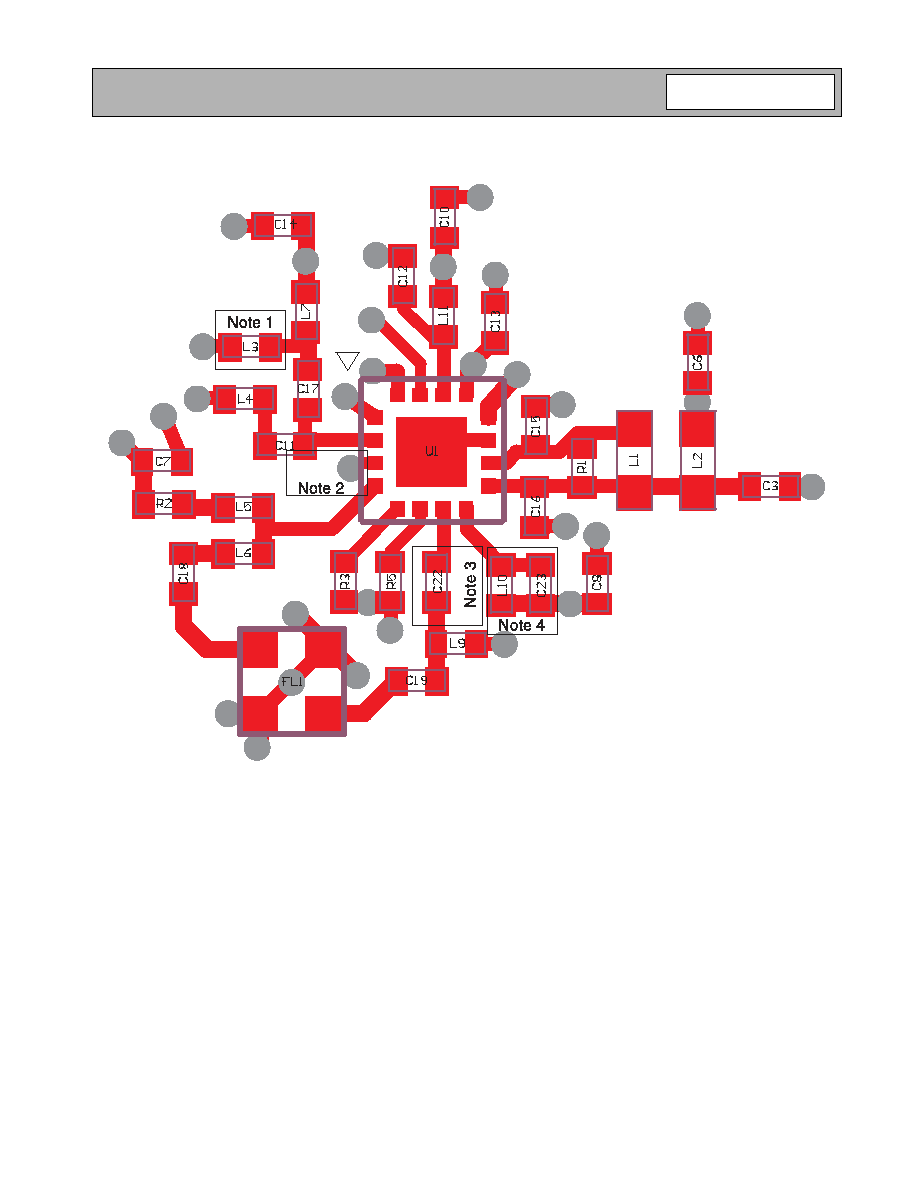
Evaluation Board Schematic
KPCS, IF=220.38MHz
(Download Bill of Materials from www.rfmd.com.)
C22
3 pF
L6
3.3 nH
C2
33 nF
L11
2.2 nH
C15
6.2 pF
R1
5.6 k
L1
100 nH
L5
15 nH
16
15
14
13
11
12
9
10
5
6
7
8
2
1
4
3
FL1
FILTER
SAWTEK
2X2
1
3
GN
D
GND
C13
10 pF
C4
33 nF
LNA GAIN
C17
33 nF
C11
DNI
L4
DNI
L3*
DNI
L7
1.5 nH
C14
1 pF
J4
LNA IN
J5
LNA OUT
R2
30
C7
33 nF
VCC
R3
8.2 k
R5
27 k
L9
33 nH
C19*
DNI
C18*
DNI
C9
33 nF
J6
MIX IN
L8
DNI
C21*
DNI
L10
3.9 nH
C23
1.3 pF
C8
33 nF
VCC
C16
6.2 pF
L2
180 nH
C6
33 nF
VCC
C3
5.1 pF
J1
CDMA IF
J2
LO IN
VCC
C12
DNI
C10
DNI
J3
LO OUT
C5
33 nF
ENABLE
C1
33 nF
TX BUF EN
*IF FREQ=220MHz
P1
3
2
1
CON3
P1-3
GN
D
GN
D
VCC
C20
1 uF
+
P2 4
3
2
1 CON4
P2-2
LNA GAIN
P2-4
TX
BUF E
N
P2-1
ENAB
LE
P3* 4
3
2
1 DNI
8-391
RF2860
Rev A7 031105
Differential IF Matching
L2, L3 and C2 are chosen to resonate at the desired IF frequency. C2 can be omitted and the value of L1 increased and
utilized solely as a choke to provide V
CC
to the open-collector outputs, but it is strongly recommended that at least some
small-valued C2 (a few pF) be retained for better mixer linearity performance. R1 is normally selected to match the input
impedance of the IF filter. However, mixer performance can be modified by selecting an R value that is different from the
IF filter input impedance, and inserting a conjugate matching network between the Resistive Output Network and the IF
filter.
C1 and C3 serve dual purposes. C1 and C3 serve as a series DC block when a DC path to ground is present in the IF fil-
ter. In addition, C1 may be chosen to improve the combine performance of the mixer and IF filter. L1 should choose to
resonate with the internal capacitance of the SAW filter. Usually, SAW filter has some capacitance. Otherwise, L1 could
be eliminated.
A practical approach to obtain the differential matching is to tune the mixer to the correct load point for gain, IIP3, and NF
using the single-end current combiner method. Second, use the component values found in the single-end approach as
starting point for the differential matching. The two-shunt capacitors in the single-end matching could be converted to a
parallel capacitor and the parallel inductor in the single-end matching needs to be converted in to a choke inductor. Third,
set the DC block capacitors (C1 and C3) in the differential-end matching to a high value (i.e., 100pF) and retune the res-
onate circuit (C2, L2 and L3) and the resistor (R) for optimal performance. After optimal performance is achieved and if
performance is not satisfactory, decrease the series capacitors until optimal performance is achieved.
C2
R1
L2
L3
V
CC
100 pF
C1
C3
IF+
IF-
L2
IF Saw
4
5
9
10
IF-
IF+

8-392
RF2860
Rev A7 031105
Single-End IF Matching
L1, C1, C2, and R form a current combiner which performs a differential to single-ended conversion at the IF frequency
and sets the output impedance. In most cases, the resonance frequency is independent of R and can be set according to
the following equation:
Where C
EQ
is the equivalent stray capacitance and capacitance looking into pins 9 and 10. An average value to use for
C
EQ
is 2.5pF.
R can then be used to set the output impedance according to the following equation:
where R
OUT
is the desired output impedance and R
P
is the parasitic equivalent parallel resistance of L1.
C
2
should first be set to 0 and C1 should be chosen as high as possible (not greater than 39pF), while maintaining an R
P
of L1 that allows for the desired R
OUT
. If the self-resonant frequencies of the selected C1 produce unsatisfactory linearity
performance, their values may be reduced and compensated for by including C2 capacitor with a value chosen to main-
tain the desired F
IF
frequency.
L2 and C3 serve dual purposes. L2 serves as an output bias choke, and C3 serves as a series DC block.
In addition, L2 and C3 may be chosen to form an impedance matching network if the input impedance of the IF filter is
not equal to R
OUT
. Otherwise, L2 is chosen to be large (suggested 120nH) and C3 is chosen to be large (suggested
22nF) if a DC path to ground is present in the IF filter, or omitted if the filter is DC-blocked.
IF-
IF+
C2
R
L1
L2
V
CC
100 pF
C3
IF Saw
4
5
9
10
IF+
IF-
C1
C1
f
IF
1
L1
2
------ C
1
2C
2
C
EQ
+
+
(
)
2
-----------------------------------------------------------
=
R
1
4 R
OUT
---------------------
1
R
P
------
≠
1
≠
=
8-393
RF2860
Rev A7 031105
RF2860 Layout Requirements
NOTES:
1. This component is not required on the evaluation board. It may be required on the phone board for optimum IIP3.
Component placeholder should be on phone board.
2. Ground for LNA emitter. For maximum gain, place ground via as close to pin 3 as possible.
3. This capacitor is required as part of the mixer input match.
4. This inductor/capacitor parallel combination is used for mixer/preamplifier interstage tuning. It must be placed
~1.6mm or closer to pin 8.
8-394
RF2860
Rev A7 031105
PCB Design Requirements
PCB Surface Finish
The PCB surface finish used for RFMD's qualification process is electroless nickel, immersion gold. Typical thickness is
3
µ
inch to 8
µ
inch gold over 180
µ
inch nickel.
PCB Land Pattern Recommendation
PCB land patterns are based on IPC-SM-782 standards when possible. The pad pattern shown has been developed and
tested for optimized assembly at RFMD; however, it may require some modifications to address company specific
assembly processes. The PCB land pattern has been developed to accommodate lead and package tolerances.
PCB Metal Land Pattern
A = 0.64 x 0.28 (mm) Typ.
B = 0.28 x 0.64 (mm) Typ.
C = 1.50 (mm) Sq.
B
B
B
B
A
A
A
A
B
B
B
B
A
A
A
A
C
Pin 16
Pin 1
Pin 12
Pin 8
Dimensions in mm.
0.50 Typ.
1.50 Typ.
0.50 Typ.
0.55 Typ.
0.55 Typ.
0.75 Typ.
0.75 Typ.
1.50
Typ.
Figure 1. PCB Metal Land Pattern (Top View)