NO
T
FOR
N
EW
DE
SI
GNS
11-121
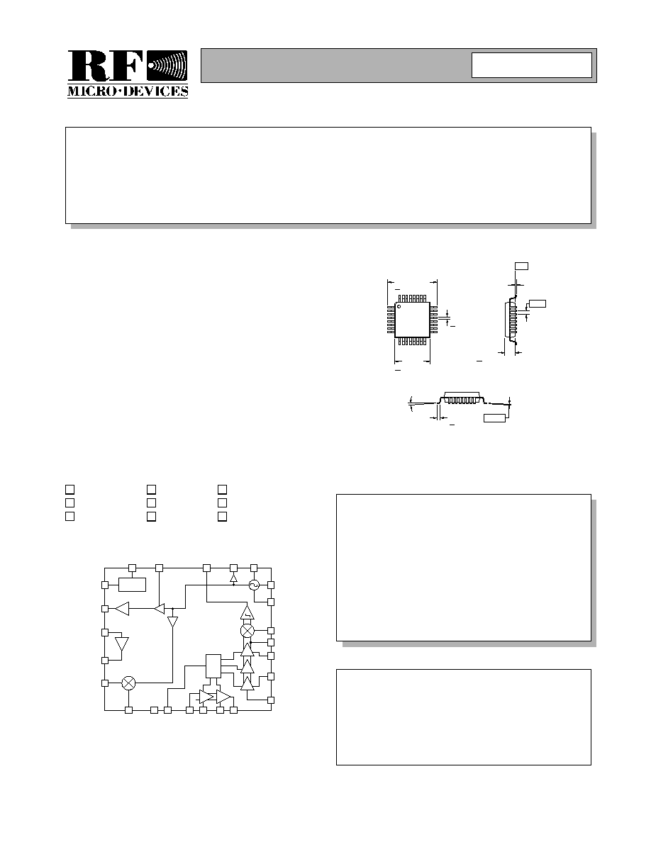
Product Description
Ordering Information
Typical Applications
Features
Functional Block Diagram
RF Micro Devices, Inc.
7628 Thorndike Road
Greensboro, NC 27409, USA
Tel (336) 664 1233
Fax (336) 664 0454
http://www.rfmd.com
Optimum Technology MatchingÆ Applied
Si BJT
GaAs MESFET
GaAs HBT
Si Bi-CMOS
SiGe HBT
Si CMOS
InGaP/HBT
GaN HEMT
SiGe Bi-CMOS
16
17
23
2
10
8
Linear
RSSI
31
LNA
6
4
1
32
26
24
25
13
VBG
19
18
11
15
14
22
21
MOD IN
IF2 IN
IF1 OU
T
CBP2-
CBP2+
V
C
O OU
T
CBP1-
CPB1+
IF1 IN
DATA O
U
T
IF2 OUT
DEMOD IN
TX OUT
MIX OU
T+
MIX IN
LNA OUT
RX IN
RESNTR+
TX ENABL
RESNTR-
29
RX ENABL
PA
CONTROL
LOGIC
LVLAD
J
RSSI
12
RF2915
433/868/915MHz FSK/ASK/OOK
TRANSCEIVER
∑ Wireless Meter Reading
∑ Keyless Entry Systems
∑ 433MHz/868MHz/915MHz ISM Band
∑ Wireless Data Transceiver
∑ Wireless Security Systems
∑ Battery-Powered Portable Devices
The RF2915 is a monolithic integrated circuit intended for
use as a low cost FM transceiver. The device is provided
in 32-lead plastic TQFP packaging and is designed to be
used with a PLL IC to provide a fully functional FM trans-
ceiver. The chip is intended for digital (ASK, FSK, OOK)
applications in the North American 915MHz ISM band
and European 433MHz/868MHz ISM band. The inte-
grated VCO has a buffered output to feed the RF signal
back to the PLL IC to form the frequency synthesizer.
Internal decoding of the RX ENABL and TX ENABL lines
allow for half-duplex operation as well as turning on the
VCO to give the synthesizer time to settle and complete
power down mode.
∑ Fully Monolithic Integrated Transceiver
∑ 2.4V to 5.0V Supply Voltage
∑ Narrowband and Wideband FSK
∑ 300MHz to 1000MHz Frequency Range
∑ 10dB Cascaded Noise Figure
∑ 10mW Output Power With Power Control
RF2915
433/868/915MHz FSK/ASK/OOK Transceiver
RF2915 PCBA-L Fully Assembled Evaluation Board (433MHZ)
RF2915 PCBA-M Fully Assembled Evaluation Board (868MHZ)
0
Rev A8 021008
7∞ MAX
0∞ MIN
+ 0.15
0.10
0.60
0.127
7.00
+ 0.20 sq.
5.00
+ 0.10 sq.
0.22
+ 0.05
Dimensions in mm.
0.15
0.05
-A-
1.40
+ 0.05
0.50
Package Style: LQFP-32_5x5
NOT FOR NEW DESIGNS
!
11-122
RF2915
Rev A8 021008
NO
T
FOR
N
EW
DE
SI
GNS
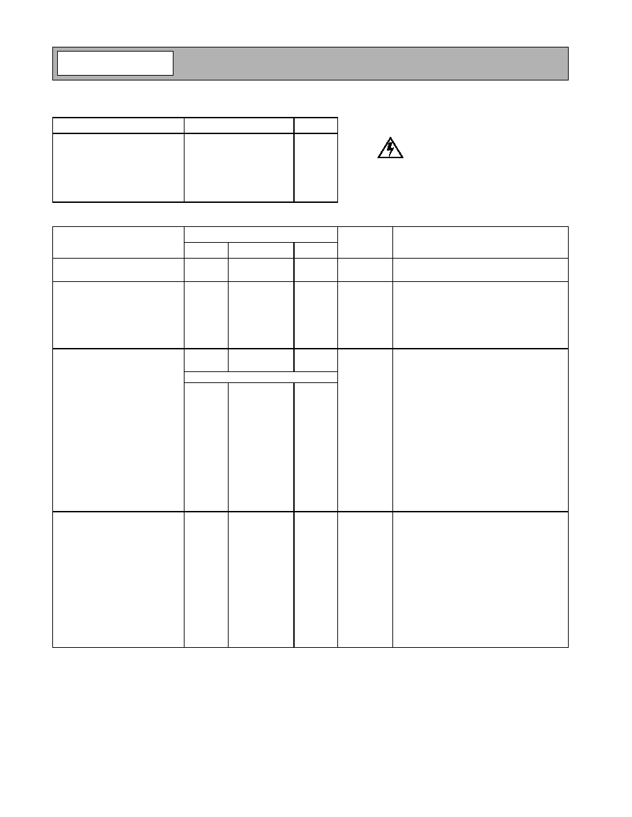
Absolute Maximum Ratings
Parameter
Ratings
Unit
Supply Voltage
-0.5 to +5.5
V
DC
Control Voltages
-0.5 to +5.0
V
DC
Input RF Level
+10
dBm
Output Load VSWR
50:1
Operating Ambient Temperature
-40 to +85
∞C
Storage Temperature
-40 to +150
∞C
Parameter
Specification
Unit
Condition
Min.
Typ.
Max.
Overall
T=25 ∞C, V
CC
=3.6V, Freq=915MHz
RF Frequency Range
300 to 1000
MHz
VCO and PLL Section
VCO Frequency Range
300 to 1000
MHz
VCO OUT Impedance
50
VCO OUT Level
-20
dBm
Freq=915MHz
VCO/PLL Phase Noise
-72
dBc/Hz
10kHz offset, Loop BW=5kHz
-98
dBc/Hz
100kHz offset, Loop BW=5kHz
Transmit Section
Max Modulation Frequency
2
MHz
Min Modulation Frequency
Set by loop filter bandwidth
Maximum Power Level
+7
+8.5
dBm
Freq=433MHz
0
+3
6
dBm
Freq=915MHz
Power Control Range
12
dB
Power Control Sensitivity
10
dB/V
Max FM Deviation
200
kHz
Instantaneous frequency deviation is
inversely proportional with the modulation
voltage. Dependent upon external circuitry.
Antenna Port Impedance
50
TX ENABL="1", RX ENABL="0"
Antenna Port VSWR
1.5:1
TX Mode
Modulation Input Impedance
4
k
Harmonics
-38
dBc
Freq=915MHz, with eval board filter
Spurious
dBc
Compliant to Part 15.249 and I-ETS 300 220
Overall Receive Section
Frequency Range
300 to 1000
MHz
Cascaded Voltage Gain
35
dB
Freq=433MHz
23
dB
Freq=915MHz
Cascaded Noise Figure
10
dB
Cascaded Input IP
3
-31
dBm
Freq=433MHz
-26
dBm
Freq=915MHz
RX Sensitivity
-95
-99
dBm
IF BW=180kHz, Freq=915MHz, S/N=8dB
LO Leakage
-55
dBm
Freq=915MHz
RSSI DC Output Range
0.5 to 2.5
V
R
LOAD
=51k
RSSI Sensitivity
22.5
mV/dB
RSSI Dynamic Range
70
80
dB
Caution! ESD sensitive device.
RF Micro Devices believes the furnished information is correct and accurate
at the time of this printing. However, RF Micro Devices reserves the right to
make changes to its products without notice. RF Micro Devices does not
assume responsibility for the use of the described product(s).

11-123
RF2915
Rev A8 021008
NO
T
FOR
N
EW
DE
SI
GNS
Parameter
Specification
Unit
Condition
Min.
Typ.
Max.
LNA
Voltage Gain
23
dB
433MHz
16
dB
915MHz
Noise Figure
4.8
dB
433MHz
5.5
dB
915MHz
Input IP
3
-27
dBm
433MHz
-20
dBm
915MHz
Input P
1dB
-37
dBm
433MHz
-30
dBm
915MHz
Antenna Port Impedance
50
RX ENABL="1", TX ENABL="0"
Antenna Port VSWR
1.5:1
RX Mode
Output Impedance
Open Collector
433MHz/915MHz
Mixer
Single-ended configuration
Conversion Voltage Gain
8
dB
433MHz
7
dB
915MHz
Noise Figure (SSB)
10
dB
433MHz
17
dB
915MHz
Input IP
3
-21
dBm
433MHz
-17
dBm
915MHz
Input P
1dB
-31
dBm
433MHz
-28
dBm
915MHz
Maximum Output Voltage
V
PP
Balanced
First IF Section
IF Frequency Range
0.1
10.7
25
MHz
Voltage Gain
34
dB
IF=10.7MHz, Z
L
=330
Noise Figure
13
dB
IF1 Input Impedance
330
IF1 Output Impedance
330
Second IF Section
IF Frequency Range
0.1
10.7
25
MHz
Voltage Gain
60
dB
IF=10.7MHz
IF2 Input Impedance
330
IF2 Output Impedance
1
k
At IF2 OUT pin
Demod Input Impedance
10
k
Data Output Impedance
1
M
Data Output Bandwidth
500
kHz
3 dB Bandwidth, Z
LOAD
=1M
|| 3pF
Data Output Level
0.3
V
CC
-0.3
V
Z
LOAD
=1M
|| 3pF; Output voltage is pro-
portional with the instantaneous frequency
deviation.

11-124
RF2915
Rev A8 021008
NO
T
FOR
N
EW
DE
SI
GNS
Parameter
Specification
Unit
Condition
Min.
Typ.
Max.
Power Down Control
Logical Controls "ON"
2.0
V
Voltage supplied to the input
Logical Controls "OFF"
1.0
V
Voltage supplied to the input
Control Input Impedance
25k
Turn On Time
1
ms
Turn on/off times are dependent upon PLL
loop parameters.
Turn Off Time
1
ms
Turn on/off times are dependent upon PLL
loop parameters.
RX to TX and TX to RX Time
100
µ
s
Power Supply
Voltage
3.6
V
Specifications
2.7 to 5.0
V
Operating limits
Temperature range -40∞C to +85∞C
2.4
V
Operating limits
Temperature range +10∞C to +40∞C
Current Consumption
18
22
27.4
mA
TX Mode, LVLADJ=3.6V
4.8
6.1
7.2
mA
TX Mode, LVLADJ=0V
4.4
5.6
6.8
mA
RX Mode
1
µ
A
Power Down Mode
3.6
mA
PLL Only Mode

11-125
RF2915
Rev A8 021008
NO
T
FOR
N
EW
DE
SI
GNS
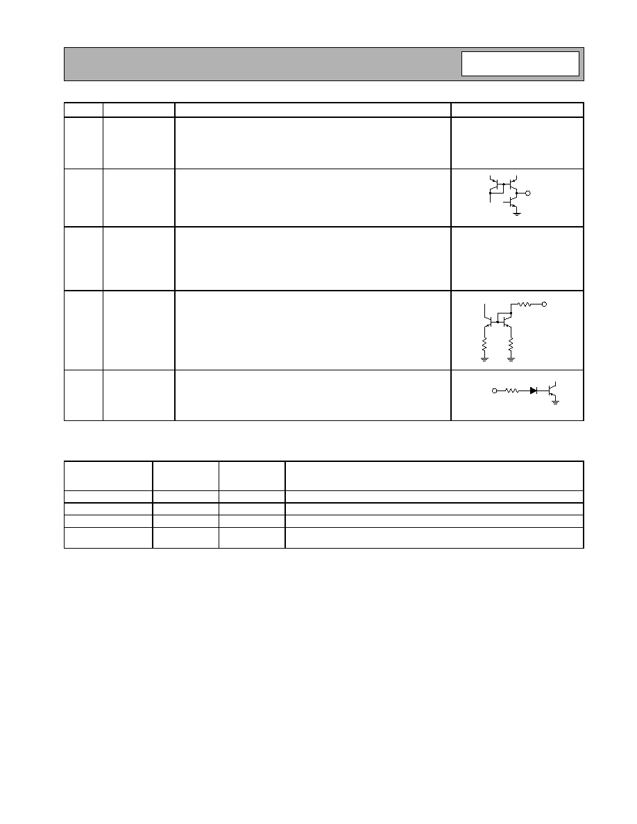
Pin
Function
Description
Interface Schematic
1
TX ENABL
Enables the transmitter circuits. TX ENABL>2.0V powers up all trans-
mitter functions. TX ENABL<1.0V turns off all transmitter functions
except the PLL functions.
2
TX OUT
RF output pin for the transmitter electronics. TX OUT output impedance
is a low impedance when the transmitter is enabled. TX OUT is a high
impedance when the transmitter is disabled.
3
GND2
Ground connection for the 40 dB IF limiting amplifier and Tx PA func-
tions. Keep traces physically short and connect immediately to ground
plane for best performance.
4
RX IN
RF input pin for the receiver electronics. RX IN input impedance is a
low impedance when the transmitter is enabled. RX IN is a high imped-
ance when the receiver is disabled.
5
GND1
Ground connection for RF receiver functions. Keep traces physically
short and connect immediately to ground plane for best performance.
6
LNA OUT
Output pin for the receiver RF low noise amplifier. This pin is an open
collector output and requires an external pull up coil to provide bias and
tune the LNA output. A capacitor in series with this output can be used
to match the LNA to 50
impedance image filters.
7
GND3
Same as pin 3.
8
MIX IN
RF input to the RF Mixer. An LC matching network between LNA OUT
and MIX IN can be used to connect the LNA output to the RF mixer
input in applications where an image filter is not needed or desired.
9
GND5
GND5 is the ground connection shared by the input stage of the trans-
mit power amplifier and the receiver RF mixer.
10
MIX OUT
IF output from the RF mixer. Interfaces directly to 10.7MHz ceramic IF
filters as shown in the application schematic. A pull-up inductor and
series matching capacitor should be used to present a 330
termina-
tion impedance to the ceramic filter. Alternately, an IF tank can be used
to tailor the IF frequency and bandwidth to meet the needs of a given
application.
11
VREF IF
DC voltage reference for the IF limiting amplifiers. A 10nF capacitor
from this pin to ground is required.
.
12
RSSI
A DC voltage proportional to the received signal strength is output from
this pin. The output voltage range is 0.5V to 2.3V and increases with
increasing signal strength.
13
IF1 IN
IF input to the 40dB limiting amplifier strip. A 10nF DC blocking capaci-
tor is required on this input.
40 k
20 k
TX ENABL
TX OUT
20
V
CC
RX IN
500
LNA OUT
V
CC
GND5
MIX IN
MIX OUT
15 pF
15 pF
GND5
GND5
V
CC
RSSI
IF1 IN
330
330
60 k
60 k
IF1 BP+
IF1 BP-

11-126
RF2915
Rev A8 021008
NO
T
FOR
N
EW
DE
SI
GNS
Pin
Function
Description
Interface Schematic
14
IF1 BP+
DC feedback node for the 40dB limiting amplifier strip. A 10nF bypass
capacitor from this pin to ground is required.
See pin 13.
15
IF1 BP-
Same as pin 14.
See pin 13.
16
IF1 OUT
IF output from the 40dB limiting amplifier. The IF1 OUT output presents
a nominal 330
output resistance and interfaces directly to 10.7MHz
ceramic filters.
17
IF2 IN
IF input to the 60dB limiting amplifier strip. A 10nF DC blocking capaci-
tor is required on this input. The IF2 IN input presents a nominal 330
input resistance and interfaces directly to 10.7MHz ceramic filters.
18
IF2 BP+
DC feedback node for the 60dB limiting amplifier strip. A 10nF bypass
capacitor from this pin to ground is required.
See pin 17.
19
IF2 BP-
Same as pin 18.
See pin 17.
20
GND6
Ground connection for 60dB IF limiting amplifier. Keep traces physically
short and connect immediately to ground plane for best performance.
21
DEMOD IN
This pin is the input to the FM demodulator. This pin is NOT AC-cou-
pled. Therefore, a DC blocking capacitor is required on this pin to avoid
shorting the demodulator input with the LC tank. A ceramic discrimina-
tor or DC blocked LC tank resonant at the IF should be connected to
this pin.
22
IF2 OUT
IF output from the 60dB limiting amplifier strip. This pin is intended to
be connected to pin 21 through a 5pF capacitor and an FM discrimina-
tor circuit.
23
MOD IN
FM analog or digital modulation can be imparted to the VCO through
this pin. The VCO varies in accordance to the voltage level presented
to this pin. To set the deviation to a desired level, a voltage divider refer-
enced to VCC is the recommended. This deviation is also dependent
upon the overall capacitance of the external resonant circuit.
See pin 24.
24
RESNTR+
This port is used to supply DC voltage to the VCO as well as to tune the
center frequency of the VCO. Equal value inductors should be con-
nected to this pin and pin 25 although a small imbalance can be used
to tune in the proper frequency range.
25
RESNTR-
See RESNTR+ description.
See pin 24.
26
VCO OUT
This pin is used is supply a buffered VCO output to go to the PLL chip.
This pin has a DC bias and needs to be AC-coupled.
27
GND4
GND4 is the ground shared on chip by the VCO, prescaler, and PLL
electronics.
IF1 OUT
IF2 IN
330
330
60 k
60 k
IF2 BP+
IF2 BP-
DEMOD IN
10 k
V
CC
IF2 OUT
RESNTR-
RESNTR+
4 k
MOD IN
VCO OUT
11-127
RF2915
Rev A8 021008
NO
T
FOR
N
EW
DE
SI
GNS
* LVL ADJ pin must be low to disable transmitter.
Pin
Function
Description
Interface Schematic
28
VCC1
This pin is used to supply DC bias to the LNA, Mixer, first IF amplifier
and Bandgap reference. A RF bypass capacitor should be connected
directly to this pin and returned to ground. A 22 pF capacitor is recom-
mended for 915MHz applications. A 68pF capacitor is recommended
for 433MHz applications.
29
DATA OUT
Demodulated data output from the demodulator. Output levels on this
are TTL/CMOS compatible. The magnitude of the load impedance is
intended to be 1M
or greater. When using a RF2915 transmitter and
receiver back to back a data inversion will occur with low side LO injec-
tion.
30
VCC3
This pin is used to supply DC bias and colletor current to the transmitter
PA. It also supplies voltage to the 2
nd
IF amplifier, Demodulator and
data slicer. A RF bypass capacitor should be connected directly to this
pin and returned to ground. A 22 pF capacitor is recommended for
915MHz applications. A 68pF capacitor is recommended for 433MHz
applications.
31
LVL ADJ
This pin is used to vary the transmitter output power. An output level
adjustment range greater than 12dB is provided through analog volt-
age control of this pin. DC current of the transmitter power amp is also
reduced with output power.
NOTE: This pin MUST be low when the transmitter is disabled.
32
RX ENABL
Enable pin for the receiver circuits. RX ENABL>2.0V powers up all
receiver functions. RX ENABL<1.0V turns off all receiver functions
except the PLL functions and the RF mixer.
Operation
Mode
TX ENABL RX ENABL
Function
Sleep Mode
Low
Low
Entire chip is powered down. Total current consumption is <1
µ
A. *
Transmit Mode
High
Low
Transmitter, VCO are on.
Receive Mode
Low
High
Receiver, VCO are on. *
PLL Lock
High
High
VCO is on. This mode allows time for a synthesizer loop to lock without
spending current on the transmitter or receiver.
DATA OUT
400
4 k
LVL ADJ
40 k
50 k
RX ENABL

11-128
RF2915
Rev A8 021008
NO
T
FOR
N
EW
DE
SI
GNS
RF2915 Theory of Operation and Application Information
The RF2915 is part of a family of low-power RF trans-
ceiver IC's that was developed for wireless data com-
munication devices operating in the European 433MHz
to 868MHz ISM band, and 915MHz U.S. ISM band.
This IC has been implemented in a 15GHz silicon
bipolar process technology that allows low-power
transceiver operation in a variety of commercial wire-
less products.
In its basic form, the RF2915 can be implemented as a
two-way half-duplex FSK transceiver with the addition
of some crystals, filters, and passive components. The
RF2915 is designed to interface with common PLL IC's
to form a multi-channel radio. The receiver IF section is
optimized to interface with low-cost 10.7MHz ceramic
filters and has a 3dB bandwidth of 25MHz and can still
be used (with lower gain) at higher frequencies with
other types of filters. The PA output and LNA input are
available on separate pins and are designed to be con-
nected together through a DC blocking capacitor. In the
transmit mode, the PA will have a 50
impedance and
the LNA will have a high impedance. In the receive
mode, the LNA will have a 50
impedance and the PA
will have a high impedance. This eliminates the need
for a TX/RX switch, and allows for a single RF filter to
be used in transmit and receive modes. Separate
access to the PA and LNA allows the RF2915 to inter-
face with external components such as a high power
PA, lower NF LNA, upconverters, and downconverters,
for a variety of implementations.
FM/FSK SYSTEMS
The MOD IN pin drives an internal varactor for modu-
lating the VCO. This pin can be driven with a voltage
level needed to generate the desired deviation. This
voltage can be carried on a DC bias to select desired
slope (deviation/volt) for FM systems. Or, a resistor
divider network referenced to VCC or ground can
divide down logic level signals to the appropriate level
for a desired deviation in FSK systems.
On the receiver demodulator, the DATA OUT pin is
generally used as a data slicer providing logic level out-
puts. However, by lightly loading the output with a
resistive load, the bandwidth of the data slicer can be
limited, and an analog signal recovered. A resistance
value of around 10k
to 15k
is sufficient. The digital
output is generated by a data slicer that is DC-coupled
differentially to the demodulator. An on-chip 1.6MHz
RC filter is provided at the demodulator output to filter
the undesirable 2xIF product. This balanced data slicer
has a speed advantage over a conventional adapter
data slicer where a large capacitor is used to provide
DC reference for the bit decision. Since a balanced
data slicer does not have to charge a large capacitor,
the RF2915 exhibits a very fast response time. For
best operation of the on-chip data slicer, FM deviation
needs to exceed the carrier frequency error anticipated
between the receiver and transmitter with margin.
The data slicer itself is a transconductance amplifier,
and the DATA OUT pin is capable of driving rail-to-rail
output only into a very high impedance and a small
capacitance. The amount of capacitance will determine
the bandwidth of DATA OUT. In a 3pF load, the band-
width is in excess of 500kHz. The rail-to-rail output of
the data slicer is also limited by the frequency deviation
and bandwidth of IF filters. With the 180kHz bandwidth
filters on the evaluation boards, the rail-to-rail output is
limited to less than 140kHz. Choosing the right IF
bandwidth and deviation versus data rate (mod index)
is important in evaluating the applicability of the
RF2915 for a given data rate.
The primary consideration when directly modulating
the VCO is the data rate versus PLL bandwidth. The
PLL will track out the modulation to the extent of its
bandwidth, which distorts the modulating data. There-
fore, the lower frequency components of the modulat-
ing data should be five to 10 times the loop bandwidth
to minimize the distortion. The lower frequency compo-
nents are generated by long strings of 1's and 0's in
data stream. By limiting the number of consecutive,
same bits, lower frequency components can be set. In
addition, the data stream should be balanced to mini-
mize distortion. Using a coding pattern such as
Manchester is highly recommended to optimize system
performance.
The PLL loop bandwidth is important in several system
parameters. For example, switching from transmit to
receive requires the VCO to retune to another fre-
quency. The switching speed is proportional to the loop
bandwidth: the higher the loop bandwidth, the faster
the switching times. Phase noise of the VCO is another
factor. Phase noise outside the bandwidth is because
of the VCO itself, rather than a crystal reference. The
design trade-offs must be made here in selecting a
PLL loop bandwidth with acceptable phase noise and
switching characteristics, as well as minimal distortion
of the modulation data.
11-129
RF2915
Rev A8 021008
NO
T
FOR
N
EW
DE
SI
GNS
ASK/OOK SYSTEMS
The transmitter of the RF2915 has an output power
level adjust (LVL ADJ) that can be used to provide
approximately 18dB of power control for amplitude
modulation. The RSSI output of the receiver section
can be used to recover the modulation. The RSSI out-
put is from a current source, and needs to have a resis-
tor to convert to a voltage. A 51k
resistor load
typically produces an output of 0.7V to 2.5V. A parallel
capacitor is suggested to band limit the signal. For
ASK applications, the 18dB range of the LVL ADJ
does not produce enough voltage swing in the RSSI for
reliable communications. The on/off keying (OOK) is
suggested to provide reliable communications. To
achieve this, the LVL ADJ and TX ENABL need to be
controlled together (please note that LVL ADJ cannot
be left high when TX ENABL is low). This will provide
an on/off ratio of greater than 50dB. One of the unfor-
tunate consequences of modulating in this manner is
VCO pulling by the PA. This results in a spurious out-
put outside the desired transmit band, as the PLL
momentarily loses lock and reacquires. This may be
avoided by pulse-shaping TX data to slow the change
in the VCO load to a pace which the PLL can track with
its given loop bandwidth. The loop bandwidth may also
be increased to allow it to track faster changes brought
about by load pulling.
For the ASK/OOK receiver demodulator, an external
data slicer is required. The RSSI output is used to pro-
vide both the filter data and a very low pass filter (rela-
tive to the data rate) DC reference to the data slicer.
Because the very low pass filter has a slow time con-
stant, a longer preamble may be required to allow for
the DC reference to acquire a stable state. Here, as in
the case of the FSK transmitter, the data pattern also
affects the DC reference and the reliability of the
receive data. Again, a coding scheme such as
Manchester should be used to improve data integrity.
APPLICATION AND LAYOUT CONSIDERATIONS
Both the RX IN and the TX OUT have a DC bias on
them. Therefore, a DC blocking cap is required. If the
RF filter has DC blocking characteristics (such as a
ceramic dielectric filter), then only one DC blocking cap
would be needed to separate the DC of the RX and TX.
These are RF signals and care should be taken to run
the signal keeping them physically short. Because of
the 50
/high impedance nature of these two signals,
they may be connected together into a single 50
device (such as a filter). An external LNA or PA may be
used, if desired, but an external RX/TX switch may be
required.
The VCO is a very sensitive block in the system. RF
signals feeding back into the VCO (either radiated or
coupled by traces) may cause the PLL to become
unlocked. The trace(s) for the anode of the tuning var-
actor should also be kept short. The layout of the reso-
nator and varactor are very important. The capacitor
and varactor should be close to the RF2915 pins, and
the trace length should be as short as possible. The
inductors may be placed further away, and reducing
the value of the inductors can compensate any trace
inductance. Printed inductors may also be used with
careful design. For best results, physical layout should
be as symmetrical as possible. Figure 1 is a recom-
mended layout pattern for the VCO components. When
using the loop bandwidth lower than 5kHz shown on
the evaluation board, better filtering of the VCC at the
resonators (and lower VCC noise, as well) will help
reduce phase noise of the VCO. A series resistor of
100
to 200
, and a 1
µ
F or larger capacitor may be
used.
For the interface between the LNA/mixer, the coupling
capacitor should be as close to the RF2915 pins as
possible, with the bias inductors further away. Once
again, the value of the inductor may be changed to
compensate for trace inductance. The output imped-
ance of the LNA is in the order of several k
, which
makes matching to 50
very difficult. If image filtering
is desired, a high impedance filter is recommended.
Not to Scale
Representative of Size
24
23
Loop
Voltage
VCC
25
26
Figure 1. Recommended VCO Layout

11-130
RF2915
Rev A8 021008
NO
T
FOR
N
EW
DE
SI
GNS
The quad tank of the discriminator may be imple-
mented with ceramic discriminator available from a
couple of sources. This design works well for wideband
applications where temperature range is limited. The
temperature coefficient of ceramic discriminators may
be in the order of +50ppm/∞C. The alternative to the
ceramic discriminator is the LC tank, which provides a
broadband discriminator more useful for high data
rates.
PLL Synthesizer
The RF2915 evaluation board uses an LMX2315 PLL
IC from National Semiconductor. This PLL IC may be
programmed from the software available from National
Semiconductor (codeloader at
www.national.com/appinfo/wireless/). An external ref-
erence oscillator is required for the PLL IC allowing for
the evaluation of different reference frequencies or
step sizes. The National Semiconductor software also
has a calculator for determining the R and C compo-
nent values for a given loop bandwidth.
The RF2915 is controlled by RX ENABL and TX
ENABL which are decoded to put the RF2915 into one
of four states. It may be put into a PLL-only mode with
TX ENABL and RX ENABL both high. This condition is
used to provide time for the synthesizer to turn on and
obtain lock before turning on the receiver or transmit-
ter. Note that LVL ADJ needs to be held low for PLL-
only mode. Sometimes, it is desirable to ramp up the
power amplifier to minimize load pulling on the VCO.
To do this with the RF2915, first put the RF2915 into
PLL mode by putting TX ENABL and RX ENABL high.
Then, ramp up LVL ADJ to turn on the transmitter and
PA. The rate at which LVL ADJ is allowed to ramp up is
dependent on the PLL loop bandwidth. VCC pushing
also affects the VCO frequency. A good low pass filter
on VCC will minimize the VCC pushing effects.

11-131
RF2915
Rev A8 021008
NO
T
FOR
N
EW
DE
SI
GNS
Pin Out
1
2
3
4
5
6
7
8
24
23
22
21
20
19
18
17
TX ENABL
TX OUT
GND2
RX IN
GND1
LNA OUT
GND3
MIX IN
RESNTR+
MOD IN
IF2 OUT
DEMOD IN
GND6
IF2 BP-
IF2 BP+
IF2 IN
32
29
30
31
GND5
MIX OUT
VREF IF
RSSI
IF1 IN
IF1 BP+
IF1 BP-
IF1 OUT
RX ENABL
LVL ADJ
VCC3
DATA OUT
VCC1
GND4
VCO OUT
RESNTR-
28
27
26
25
9
12
11
10
13
14
15
16

11-132
RF2915
Rev A8 021008
NO
T
FOR
N
EW
DE
SI
GNS
915 MHz Application Schematic
16
17
23
2
10
8
Linear
RSSI
31
LNA
6
4
1
32
26
24
25
13
19
18
11
15
14
22
21
29
PA
Control
Logic
12
3
5
7
9
20
30
28
27
Gain
Control
915 MHz SAW
22 pF
10 nH
10 pF
V
CC
8.2 uH
22 pF
V
CC
100 pF
100 pF
11 pF
10
10 nF
10
10 nF
RX ENABL
TX ENABL
Filter
10 nF10 nF
51 k
10 pF
RSSI
Filter
5 pF
FM Disc.
1.5 k
10 nF
10 nF
10 nF
MOD IN
22
k
220
pF
2.2 nF
10 k
33 pF
PLL
IC
22 pF
10 nF 10
V
CC
22 pF
4.7 nH
4.7 nH
4 pF
10 nF
100
V
CC
D1
SMV1234
-011
22 pF
10 nF
10
V
CC
LVL ADJ
DATA OUT
PLL LOOP BANDWIDTH ~10 kHz

11-133
RF2915
Rev A8 021008
NO
T
FOR
N
EW
DE
SI
GNS
Evaluation Board Schematic
(Download Bill of Materials from www.rfmd.com.)
16
17
23
2
10
8
Linear
RSSI
31
LNA
6
4
1
32
24
25
13
19
18
11
15
14
22
21
29
PA
Control
Logic
12
3
5
7
9
20
30
28
27
Gain
Control
C22
22 pF
L4**
C21**
L5
8.2
µ
H
C25
22 pF
V
CC
C6 22 pF
C7 22 pF
C24
11 pF
R7
10
C23
10 nF
RX ENABL
P3-3
TX ENABL
P3-2
F1
SFECV10.7
MS3S-A-TC
R3
51 k
C13
10 pF
P4-1
RSSI
F2
SFECV10.7
MS3S-A-TC
C19
5 pF
U4
CDF107B-
A0
R5
1.5 k
C20
10 nF
C15 10 nF
C14 10 nF
R13
1.2
k
C47
6.8 nF
C48
0.1
µ
F
R14
10 k
C50
22 pF
C3
0.1
µ
F
R2
10
V
CC
C17 22 pF
L3**
L2**
C16**
C18 0.1
µ
F
R4
100
V
C
C
D1**
C2
0.1
µ
F
R1
10
V
CC
P2-1
LVL ADJ
PLL LOOP BW ~5 kHz
1
2
3
4
5
6
7
8
9
10
20
19
18
17
16
15
14
13
12
11
OSC IN
NC
OSC OUT
VP
VCC
DO
GND
LD
NC
F IN
PHS R
PWRD
N
PHS P
F OUT
BI SW
FC
LE
DATA
NC
CLK
C47 22 pF
C43
10 nF
V
PLL
R60
0
L7*
TBD
C49*
X1*
10 MHz
C42 10 nF
C41
10 nF
R30*
0
R15
0
J5
REF OSC
V
PLL
R27
12 k
R28
12 k
R29
12 k
R24
27 k
R25
27 k
R26
27 k
1
2
3
4
5
6
7
8
9
10
NC
P5-2
P5-3
P5-4
NC
NC
NC
NC
NC
Enable (PLL IC)
Data (PLL IC)
Clock (PLL IC)
GND
P5
P4-1
P4
RSSI
GND
1
2
P3-3
P3
1
2
3
4
5
TX ENABL
GND
RX ENABL
P3-2
NC
NC
P3-5
P3-4
V
PLL
(LMX2315)
V
CC
(RF2915)
P1-1
P1-3
P1
GND
1
2
3
P2-1
P2-3
P2
GND
1
2
3
LVL ADJ
NC
C81
4.7
µ
F
C1
22 pF
C4
22 pF
C30**
L8/R80**
C8**
L1**
C9**
J2
RF
R6*
N/C
C10
10 nF
C12
10 nF
C13
10 nF
J1
RX OUT
J4
MOD IN
C29
4.7
µ
F
C5
4.7
µ
F
C27*
10 nF
L6*
2.2
µ
H
C28*
120 pF
J3
MIX OUT
* Denotes components that are normally depopulated.
V
CC
LMX2315
** Component values for the different eval versions:
26
P6
DB9
5
9
4
7
6
1
2
3
8
R8
3.2 k
R9
10
C26
10 nF
22 nH
8.2 nH
8.2 nH
L1
22 nH
jumper
jumper
L8/R80
8 pF
4 pF
4 pF
C9
15 pF
4 pF
4 pF
C8
8 pF
N/C
N/C
C30
47 nH
12 nH
10 nH
L4
433 MHz
868 MHz
915 MHz
Freq
33 pF
9 pF
10 pF
C21
15 nH
4.7 nH
8.2 nH
L2/L3
7 pF
5 pF
1.5 pF
C16
SMV-1235-011 (Alpha)
SMV-1234-011 (Alpha)
SMV-1233-011 (Alpha)
D1

11-134
RF2915
Rev A8 021008
NO
T
FOR
N
EW
DE
SI
GNS
Evaluation Board Layout
Board Size 3.070" x 3.670"
Same board layout is used for the -L, -M, and -H versions

11-135
RF2915
Rev A8 021008
NO
T
FOR
N
EW
DE
SI
GNS

11-136
RF2915
Rev A8 021008
NO
T
FOR
N
EW
DE
SI
GNS

11-137
RF2915
Rev A8 021008
NO
T
FOR
N
EW
DE
SI
GNS
TX Power Output and I
CC
versus Level Adjust
at 433MHz, 3.6V V
CC
-15.0
-10.0
-5.0
0.0
5.0
10.0
0.0
0.5
1.0
1.5
2.0
2.5
3.0
3.5
4.0
LVL ADJ (V)
RF P
0
(dBm)
5.0
10.0
15.0
20.0
25.0
30.0
Pout(433)
Icc(433)
TX Power Output and I
CC
versus Level Adjust
at 868MHz, 3.6V V
CC
-20.0
-15.0
-10.0
-5.0
0.0
5.0
0.0
0.5
1.0
1.5
2.0
2.5
3.0
3.5
4.0
LVL ADJ (V)
RF P
0
(dBm)
5.0
10.0
15.0
20.0
25.0
30.0
I
CC
(mA)
Pout(868)
Icc(868)
TX Power Output and I
CC
versus Level Adjust
at 905MHz, 3.6V V
CC
-20.0
-15.0
-10.0
-5.0
0.0
5.0
0.0
0.5
1.0
1.5
2.0
2.5
3.0
3.5
4.0
LVL ADJ (V)
RF P
0
(dBm)
5.0
10.0
15.0
20.0
25.0
30.0
I
CC
(mA)
Pout(905)
Icc(905)
Receive Current versus V
CC
(including LMX2315 IC)
4.0
5.0
6.0
7.0
8.0
9.0
2.5
3.0
3.5
4.0
4.5
5.0
5.5
Supply Voltage (V)
I
CC
(mA)
Icc (433)
Icc (868)
Icc (905)
RSSI versus RF Input
0.0
0.5
1.0
1.5
2.0
2.5
3.0
-120.0
-110.0
-100.0
-90.0
-80.0
-70.0
-60.0
-50.0
-40.0
RF Input (dBm)
RSSI (V)
433 MHz
868,905 MHz
RSSI Output versus Temperature
V
CC
= 2.4V
0.0
0.5
1.0
1.5
2.0
2.5
-130.0
-110.0
-90.0
-70.0
-50.0
-30.0
-10.0
10.0
Received Signal Strength (dBm)
RSSI Output (V)
-40∞C
10∞C
25∞C
40∞C
85∞C

11-138
RF2915
Rev A8 021008
NO
T
FOR
N
EW
DE
SI
GNS