 | –≠–ª–µ–∫—Ç—Ä–æ–Ω–Ω—ã–π –∫–æ–º–ø–æ–Ω–µ–Ω—Ç: RF2942 | –°–∫–∞—á–∞—Ç—å:  PDF PDF  ZIP ZIP |
11-195
Product Description
Ordering Information
Typical Applications
Features
Functional Block Diagram
RF Micro Devices, Inc.
7628 Thorndike Road
Greensboro, NC 27409, USA
Tel (336) 664 1233
Fax (336) 664 0454
http://www.rfmd.com
Optimum Technology MatchingÆ Applied
Si BJT
GaAs MESFET
GaAs HBT
Si Bi-CMOS
SiGe HBT
Si CMOS
InGaP/HBT
GaN HEMT
SiGe Bi-CMOS
3
I D
A
TA-
I D
A
TA+
4
LO IN+
12
14
TX
E
N
1
Q DATA-
2
Q DAT
A
+
9 RF OUT
+45∞
-45∞
˜2
LO2 OUT 15
RF2942
UHF QUADRATURE MODULATOR
AND TRANSMITTER
∑ 915MHz ISM Band Products
∑ Digital Communications
∑ Quadrature Modulation
∑ Portable Battery-Powered Equipment
The RF2942 is an integrated power amplifier and quadra-
ture modulator IC. The quadrature modulator is driven
with a single-ended local oscillator (LO) source. The
quadrature phase generation of the LO is accomplished
using an internal passive network tuned for twice the
operating frequency. The LO frequency is at twice the RF
frequency to avoid interfering with an external synthe-
sizer.
∑ 2.0V to 3.6V Power Supply
∑ 902MHz to 928MHz Frequency Range
∑ 200mW Output Power
∑ Low LO Input Level
∑ Low Broadband Noise Floor
∑ Small Footprint
RF2942
UHF Quadrature Modulator and Transmitter
RF2942 PCBA
Fully Assembled Evaluation Board
0
Rev A4 040115
12∞
MAX
SEATING
PLANE
-C-
0.05
0.01
0.80
0.65
0.05 C
1.00
0.85
0.10
C A B
M
0.35
0.23
0.60
0.24
TYP
0.75
0.50
1.85
1.55
SQ.
0.65
0.23
0.13
4 PLCS
0.65
0.30
4 PLCS
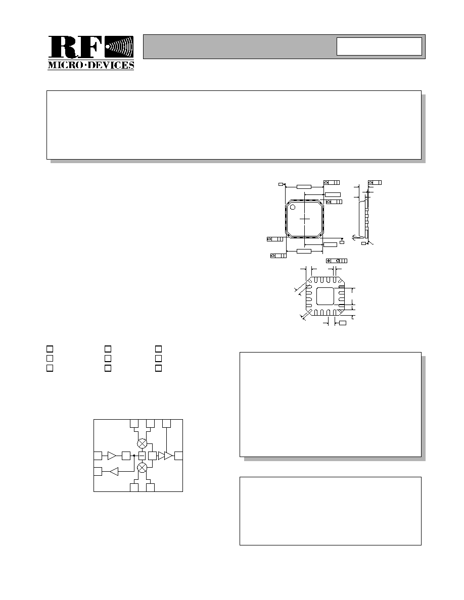
Shaded lead is pin 1.
Dimensions in mm.
4.00 SQ.
2.00 TYP
3.75 SQ.
-B-
-A-
0.25 C A
2 PLCS
0.25 C B
2 PLCS
0.20 C A
2 PLCS
0.20 C B
2 PLCS
1.88 TYP
Package Style: QFN, 16-Pin, 4x4

11-196
RF2942
Rev A4 040115
Absolute Maximum Ratings
Parameter
Rating
Unit
Supply Voltage
-0.5 to +3.6
V
DC
Power Down Voltage (V
PD
)
V
CC
+0.4
V
DC
Input LO and RF Levels
+6
dBm
Operating Ambient Temperature
-40 to +85
∞C
Storage Temperature
-40 to +150
∞C
Parameter
Specification
Unit
Condition
Min.
Typ.
Max.
Power Supply
Voltage
2.8
V
Specifications
2.0
3.6
V
Operating limits
Current
170
225
260
mA
10
24
mA
TXEN=0.0V
Carrier Input (LO IN)
T=25 ∞C, V
CC
=2.8V
Frequency Range
1800 to 1860
MHz
Power Level
-15
-6
dBm
Input Impedance
50
1830MHz
Modulation Input
Frequency Range
DC
2
10
MHz
50
source, I,Q=400mV
p-p
Modulation for P
OUT
Power (I & Q)
400
mV
P-P
Differential
Quadrature Phase Error
+2
+5
∞
I/Q Amplitude Imbalance
0.2
dB
Input Impedance
>10
k
RF Output
T=25∞C, V
CC
=2.8V, LO power=-6dBm,
SSB, I/Q=400mV
P-P
sine wave, 500kHz
Power Output
23
dBm
V
CC
=3.0V
21
22
27
dBm
V
CC
=2.8V
Second Harmonic Output
-20
-25
dBc
Third Harmonic Output
-35
-45
dBc
Sideband Suppression
-25
-40
dBc
Carrier Suppression
-25
dBc
Modulation DC offset can be externally
adjusted for optimum suppression. Carrier
suppression is then typically better than
40dB.
Broadband Noise Floor
-90
dBm/Hz
Caution! ESD sensitive device.
RF Micro Devices believes the furnished information is correct and accurate
at the time of this printing. However, RF Micro Devices reserves the right to
make changes to its products without notice. RF Micro Devices does not
assume responsibility for the use of the described product(s).

11-197
RF2942
Rev A4 040115
Pin
Function
Description
Interface Schematic
1
QSIG-
Reference voltage for the I and Q mixer. This voltage should be the
same as the DC voltage supplied to the I and Q SIG pin. To obtain a
carrier suppression of better than 40dB it may be tuned ±0.15V (rela-
tive to the I and Q SIG DC voltage). Without tuning, the carrier suppres-
sion will typically be better than 25dB. The input impedance of this pin
is typically >10 k
.
2
QSIG+
Same as pin 1, except complementary input.
See pin 1.
3
ISIG-
Same as pin 4, except complementary input.
See pin 1.
4
ISIG+
This pin is used to supply V
cc
to the modulator circuits. A RF bypass
capacitor should be connected directly to this and ground. Baseband
input to the I mixer. A DC bias of approximately 1.2V is present at this
pin.A DC blocking capacitor is needed if the signal has a different DC
level. Maximum output power is obtained when the input signal has a
peak to peak amplitude of 1V. The input impedance of this pin is about
3 k
. The SIG- and SIG+ inputs are interchangeable. If swapping the I
SIG+ and I SIG- pins, the Q SIG+ and Q SIG- also need to be swapped
to maintain the correct phase. The SIG+ and SIG- pins may be driven
differentially for BPSK to increase conversion gain.
See pin 1.
5
N/C
No connection.
6
GND
7
PA VCC
Voltage supply for PA driver.
8
N/C
No connection.
9
RF OUT
Power Amp output, open collector output.
10
N/C
No connection.
11
VCC3
Voltage supply for PA buffer.
12
TX EN
TX enabled when >2.0V. When TX EN is held low, only the LO buffer,
LO divider and LO divider buffer are left on. To power all of the circuitry
down, TX EN and VCC1 must be held low.
13
VCC1
Voltage supply for LO buffer and divider.
14
LO IN
The LO input level should be greater than -15dBm for proper operation.
15
LO/2 OUT
LO divide-by-2 output.
16
VCC2
Voltage supply for mixers.
DATA
DATA+
BIAS
VCC3 RF OUT
BIAS
LO IN-
LO IN+

11-198
RF2942
Rev A4 040115
Pin Out
VC
C1
QSIG- 1
NC
RF OUT
2
3
4
12
11
10
9
16
15
14
13
5
6
7
8
QSIG+
ISIG-
ISIG+
PA GN
D
PA VCC
NC
NC
VCC3
TX EN
LO IN
LO DIV
2
VCC
2

11-199
RF2942
Rev A4 040115
Theory of Operation
Modulator
The modulator is a direct conversion double balanced
quadrature mixer architecture. The local oscillator sig-
nal is buffered then split with internal phase shifters
that are optimized for twice the operating frequency.
The LO buffer provides isolation from load changes
that may occur as the power amplifier section is turned
on and off. In addition, the LO buffer may be left on
when the transmit section is turned off to prevent load
pulling of the external oscillator, by holding TX EN low
and leaving the bias on VCC1.
The baseband I and Q pins are connected to the inter-
nal mixer bias, therefore it is recommended that the
modulation signal be DC-blocked if a similar external
reference voltage cannot be provided. The baseband
drive may be either single-ended with the complemen-
tary input AC-grounded with a capacitor or driven dif-
ferentially.
Power Amplifier
The power amplifier requires matching on the output
(RF OUT) and the interstage transistor (PA VCC).

11-200
RF2942
Rev A4 040115
Evaluation Board Schematic - 915MHz
(Download Bill of Materials from www.rfmd.com).
5
6
7
8
9
2
3
4
12
11
10
13
14
15
16
1
C21
22 pF
C22
22nF
C19
22 pF
C20
5.0 pF
L5
18 nH
VCC5
C16
22 pF
C17
22 nF
C14
22 pF
C15
22 nF
TX EN
C11
22 pF
C12
22 nF
L3
3.3 nH
L2
56 nH
C9
5 pF
C10
22 pF
C7
22 pF
C8
22 nF
L1
5.6 nH
C5
22 pF
C6
22 nF
PA VCC
R1
15 k
R2
10 k
C1
0.1 nF
R9
160
R10
2
J4
Q SIG-
VCC5
R3
15 k
R4
10 k
C2
0.1 nF
J5
Q
SIG+
VCC5
R5
15 k
R6
10 k
C3
0.1 nF
J6
I SIG-
VCC5
R7
15 k
R8
10 k
C4
0.1 nF
J7
I
SIG+
VCC4
J3
RF OUT
VCC3
VCC2
J1
LO
DIV2
C18
0.5 pF
L4
6.8 nH
J2
LO
VCC1
P3
1
2
3
CON3
P3-1
VCC3
GND
P3-3
VCC4
P2
1
2
CON2
P2-1
PA VCC
GND
P4
1
2
3
CON3
P4-1
VCC1
GND
P4-3
TX EN
VCC2
P1
1
2
CON2
P1-1
GND
P5
1
2
CON2
P5-1
GND
VCC5

11-201
RF2942
Rev A4 040115
Evaluation Board Layout
Board Size 1.4" x 1.5"
Board Thickness 0.032", Board Material FR-4, Multi-Layer

11-202
RF2942
Rev A4 040115
Graphs
Unless swept, the conditions for the subsequent graphs are as follows. All cable losses accounted for in measurements.
VCC=2.8V
I/Q Frequency=1MHz
LO Frequency=1830MHz
I/Q Amplitude=400mV
P-P
LO Amplitude=-6dBm
I/Q Phase=90∞
P
OUT
versus V
CC
Over Temperature
15.0
16.0
17.0
18.0
19.0
20.0
21.0
22.0
23.0
24.0
25.0
26.0
27.0
28.0
29.0
30.0
2.0
2.2
2.4
2.6
2.8
3.0
3.2
3.4
3.6
V
CC
(V)
P
OUT
(dBm)
-40.0∞C
25.0∞C
85.0∞C
P
OUT
versus LO Amplitude Over Temperature
20.0
20.5
21.0
21.5
22.0
22.5
23.0
23.5
24.0
24.5
25.0
-15.0
-12.0
-9.0
-6.0
-3.0
0.0
LO Amplitude (dBm)
P
OUT
(dBm)
-40.0∞C
25.0∞C
85.0∞C
P
OUT
versus LO Frequency Over Temperature
20.0
20.5
21.0
21.5
22.0
22.5
23.0
23.5
24.0
24.5
25.0
1800.0
1810.0
1820.0
1830.0
1840.0
1850.0
1860.0
LO Frequency (MHz)
P
OUT
(dBm)
-40.0∞C
25.0∞C
85.0∞C
P
OUT
versus I/Q Amplitude Over Temperature
20.0
20.5
21.0
21.5
22.0
22.5
23.0
23.5
24.0
24.5
25.0
250.0 300.0 350.0 400.0 450.0 500.0 550.0 600.0 650.0 700.0 750.0
I/Q Amplitude (mV
P-P
)
P
OU
T
(dBm)
-40.0∞C
25.0∞C
85.0∞C

11-203
RF2942
Rev A4 040115
P
OUT
2f0 versus V
CC
Over Temperature
-28.5
-28.0
-27.5
-27.0
-26.5
-26.0
-25.5
-25.0
-24.5
-24.0
-23.5
2.0
2.2
2.4
2.6
2.8
3.0
3.2
3.4
3.6
V
CC
(V)
P
OUT
2f0 (dBc)
-40.0∞C
25.0∞C
85.0∞C
P
OUT
3f0 versus V
CC
Over Temperature
-70.0
-60.0
-50.0
-40.0
-30.0
-20.0
-10.0
0.0
2.0
2.2
2.4
2.6
2.8
3.0
3.2
3.4
3.6
V
CC
(V)
P
OUT
3f0 (dBc)
-40.0∞C
25.0∞C
85.0∞C
Carrier Suppression versus V
CC
Over Temperature
-40.0
-35.0
-30.0
-25.0
-20.0
-15.0
-10.0
-5.0
0.0
2.0
2.2
2.4
2.6
2.8
3.0
3.2
3.4
3.6
V
CC
(V)
Carrier Suppression (dBc)
-40.0∞C
25.0∞C
85.0∞C
Carrier Suppression versus LO Amplitude Over
Temperature
-35.0
-30.0
-25.0
-20.0
-15.0
-10.0
-5.0
0.0
-15.0
-12.0
-9.0
-6.0
-3.0
0.0
LO Amplitude (dBm)
Carrier Suppression (dBc)
-40.0∞C
25.0∞C
85.0∞C
Idle Current versus V
CC
Over Temperature
0.0
50.0
100.0
150.0
200.0
250.0
300.0
350.0
2.0
2.2
2.4
2.6
2.8
3.0
3.2
3.4
3.6
V
CC
(V)
Idle Current (mA)
-40.0∞C
25.0∞C
85.0∞C
I
CC
versus V
CC
Over Temperature
0.0
50.0
100.0
150.0
200.0
250.0
300.0
350.0
2.0
2.2
2.4
2.6
2.8
3.0
3.2
3.4
3.6
V
CC
(V)
I
CC
(mA)
-40.0∞C
25.0∞C
85.0∞C

11-204
RF2942
Rev A4 040115
Carrier Suppression versus I/Q Phase Over Temperature
-35.0
-30.0
-25.0
-20.0
-15.0
-10.0
-5.0
0.0
80.0
85.0
90.0
95.0
100.0
I/Q Phase (degrees)
Carrier Suppression (dBc)
-40.0∞C
25.0∞C
85.0∞C
Image Suppression versus V
CC
Over Temperature
-60.0
-55.0
-50.0
-45.0
-40.0
-35.0
-30.0
-25.0
-20.0
-15.0
-10.0
-5.0
0.0
5.0
2.0
2.2
2.4
2.6
2.8
3.0
3.2
3.4
3.6
V
CC
(V)
Image Suppression (dBc)
-40.0∞C
25.0∞C
85.0∞C
Image Suppression versus LO Amplitude Over
Temperature
-50.0
-45.0
-40.0
-35.0
-30.0
-25.0
-20.0
-15.0
-10.0
-5.0
0.0
-15.0
-12.0
-9.0
-6.0
-3.0
0.0
LO Amplitude (dBm)
Image Suppression (dBc)
-40.0∞C
25.0∞C
85.0∞C
Image Suppression versus LO Frequency Over
Temperature
-50.0
-45.0
-40.0
-35.0
-30.0
-25.0
-20.0
-15.0
-10.0
-5.0
0.0
1800.0
1810.0
1820.0
1830.0
1840.0
1850.0
1860.0
LO Frequency (MHz)
Image Suppression (dBc)
-40.0∞C
25.0∞C
85.0∞C
Carrier Suppression versus LO Frequency Over
Temperature
-35.0
-30.0
-25.0
-20.0
-15.0
-10.0
-5.0
0.0
1800.0
1810.0
1820.0
1830.0
1840.0
1850.0
1860.0
LO Frequency (MHz)
Carrier Suppression (dBc)
-40.0∞C
25.0∞C
85.0∞C
Carrier Suppression versus I/Q Amplitude Over
Temperature
-40.0
-35.0
-30.0
-25.0
-20.0
-15.0
-10.0
-5.0
0.0
250.0
375.0
500.0
625.0
750.0
I/Q Amplitude (mV
P-P
)
Carrier Suppression (dBc)
-40.0∞C
25.0∞C
85.0∞C

11-205
RF2942
Rev A4 040115
LODiv2 Out versus V
CC
Over Temperature
-12.0
-11.0
-10.0
-9.0
-8.0
-7.0
-6.0
-5.0
-4.0
-3.0
-2.0
-1.0
0.0
2.0
2.2
2.4
2.6
2.8
3.0
3.2
3.4
3.6
V
CC
(V)
LO Div2 Out (dBm)
-40.0∞C
25.0∞C
85.0∞C
LODiv2 Out versus LO Amplitude Over Temperature
-12.0
-10.0
-8.0
-6.0
-4.0
-2.0
0.0
-15.0
-12.0
-9.0
-6.0
-3.0
0.0
LO Amplitude (dBm)
LODiv2 Out (dBm)
-40.0∞C
25.0∞C
85.0∞C
LODiv2 Out versus LO Frequency Over Temperature
-12.0
-11.0
-10.0
-9.0
-8.0
-7.0
-6.0
-5.0
-4.0
-3.0
-2.0
-1.0
0.0
1800.0
1810.0
1820.0
1830.0
1840.0
1850.0
1860.0
LO Frequency (MHz)
LO Div2 Out (dBm)
-40.0∞C
25.0∞C
85.0∞C
LODiv2 Out versus I/Q Amplitude Over Temperature
-12.0
-11.0
-10.0
-9.0
-8.0
-7.0
-6.0
-5.0
-4.0
-3.0
-2.0
-1.0
0.0
250.0
375.0
500.0
625.0
750.0
I/Q Amplitude (mV
P-P
)
LO Div2 Out (dBm)
-40.0∞C
25.0∞C
85.0∞C
Image Suppression versus I/Q Amplitude Over
Temperature
-50.0
-45.0
-40.0
-35.0
-30.0
-25.0
-20.0
-15.0
-10.0
-5.0
0.0
250.0 300.0 350.0 400.0 450.0 500.0 550.0 600.0 650.0 700.0 750.0
I/Q Amplitude (mV
P-P
)
Image Suppression (dBc)
-40.0∞C
25.0∞C
85.0∞C
Image Suppression versus I/Q Phase Over Temperature
-70.0
-60.0
-50.0
-40.0
-30.0
-20.0
-10.0
0.0
80.0
85.0
90.0
95.0
100.0
I/Q Phase (degree)
Image Suppression (dBc)
-40.0∞C
25.0∞C
85.0∞C

11-206
RF2942
Rev A4 040115