 | –≠–ª–µ–∫—Ç—Ä–æ–Ω–Ω—ã–π –∫–æ–º–ø–æ–Ω–µ–Ω—Ç: RF2958 | –°–∫–∞—á–∞—Ç—å:  PDF PDF  ZIP ZIP |

11-263
Product Description
Ordering Information
Typical Applications
Features
Functional Block Diagram
RF Micro Devices, Inc.
7628 Thorndike Road
Greensboro, NC 27409, USA
Tel (336) 664 1233
Fax (336) 664 0454
http://www.rfmd.com
Optimum Technology MatchingÆ Applied
Si BJT
GaAs MESFET
GaAs HBT
Si Bi-CMOS
SiGe HBT
Si CMOS
InGaP/HBT
GaN HEMT
SiGe Bi-CMOS
RX I
I BYP
RX Q
Q BYP
VCC BB
TX
I
TX Q
IF IN+
IF IN-
VCC IF
IF OUT+
IF OUT-
TX
V
G
C
RF
OUT
RF
IN
LN
A
G
S
MODE
1
MODE0
MCLK
VCC PLL4
SDI
R BIAS
VCC RF2
VCC RF1
V
CC R
F
3
V
CC PL
L
1
PL
L RE
G
DIG REG
VREF
RX VGC
SCLK
SSB
3rd Order
Bes LPF
3rd Order
Bes LPF
3rd Order
Bes LPF
3rd Order
Bes LPF
IF Synth Analog
RF PLL
Voltage
Regulator
RX IF
Voltage
Regulator 1
RX IF
Voltage
Regulator 2
D/A
MUX
LC Trap
RF Synth Analog
RF PLL
Voltage
Regulator
Digital
Voltage
Regulator
SPI Serial Port
Frac-N Digital
P & R
11
31
30
29
28
27 26
25
1
32
2
3
6
7
8
5
4
12
13
14
15
16
22
23
24
17
21
20
19
18
9
10
RF2958
2.4GHz SPREAD-SPECTRUM TRANSCEIVER
∑ IEEE 802.11b WLANs
∑ Wireless Residential Gateways
∑ Secure Communication Links
∑ High Speed Digital Links
∑ Wireless Security
∑ Digital Cordless Telephones
The RF2958 is a single-chip transceiver specifically
designed for IEEE 802.11b applications. The part
includes all required transceiver functions. The receiver
includes: an LNA and downconverter; complete synthe-
sizers and VCO's; direct conversion from IF receiver with
variable gain control; quadrature demodulator; I/Q base-
band amplifiers; and, on-chip baseband filters. For the
transmit side, a QPSK modulator and upconverter are
provided along with the synthesizer, VCO, and PA driver.
A minimum number of external components are required,
resulting in an ultra-compact low-cost radio design. Two-
cell or regulated three-cell (3.6V maximum) battery appli-
cations are supported by the part. The RF2958 is also
part of a 2.4GHz chipset along with our high-efficiency
GaAs HBT PA and the RF3002 Baseband Processor.
∑ Complete IEEE802.11b Transceiver
including VCOs
∑ Small 32-pin Leadless Package
∑ Minimal External Components Required
∑ Low Receive Current
∑ High Performance Super-het Architecture
RF2958
2.4GHz Spread-Spectrum Transceiver
RF2958TR13
2.4GHz Spread-Spectrum Transceiver (Tape & Reel)
RF2958 PCBA
Fully Assembled Evaluation Board
0
Rev A0 050209
5.000
± 0.050
5.000
± 0.050
SEATING
PLANE
SCALE:
NONE
0.080 C
0.025
± 0.010
0.100
C
M
-C-
0.900
± 0.070
3.400
0.400
± 0.050 TYP
0.500
TYP
3.400
Shaded lead is pin 1.
Dimensions in mm.
Package Style: QFN, 32-Pin, 5x5

11-264
RF2958
Rev A0 050209
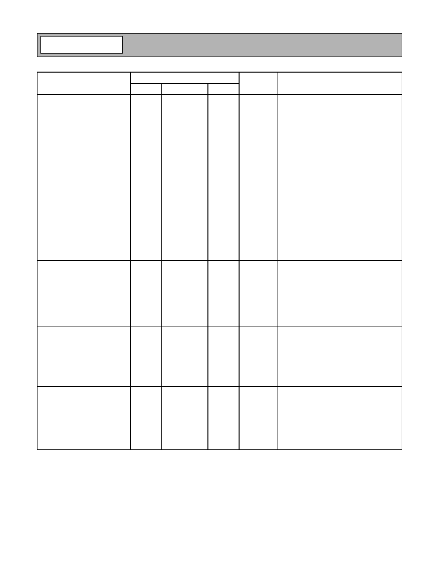
Absolute Maximum Ratings
Parameter
Rating
Unit
Supply Voltage
-0.5 to +3.6
V
DC
Control Voltages
-0.5 to +3.6
V
DC
Input RF Level
+12
dBm
Operating Ambient Temperature
-40 to +85
∞C
Storage Temperature
-40 to +150
∞C
Parameter
Specification
Unit
Condition
Min.
Typ.
Max.
Receiver LNA/RF
V
CC
=3.0V, T=+25∞C, MCLK=44MHz,
unless otherwise specified
RF Frequency Range
2400
2500
MHz
IF Frequency Range
363
385
MHz
374MHz ±11MHz
Voltage Gain - High
32
(20dB
power)
35
(23dB
power)
38
(26dB
power)
dB
LNA/mixer voltage gain (Note: into output
impedance). LNA/mixer/SAW filter voltage
gain. LNA GS=1
Voltage Gain - Low
-1
(-13dB
power)
+2
(-10dB
power)
+5
(-7dB
power)
dB
LNA/mixer voltage gain. LNA GS=0
Noise Figure - High Gain
4
dBm
Noise Figure - Low Gain
32
dBm
Input IP3 - High Gain
-23
dBm
Input IP3 - Low Gain
+8
dBm
Input P1dB - High Gain
-30
dBm
Input P1dB - Low Gain
-2
dBm
Input Return Loss
10
dB
Z
0
=50
Output Impedance
750
Image Rejection
30
dB
Receiver
IF VGA/Baseband
IF Frequency Range
374
MHz
IF Input Impedance
750
Voltage Gain - High
70
dB
V
GC
=1.25V (measured to single-ended out-
put)
Voltage Gain - Low
4
dB
V
GC
=1.95V (measured to single-ended out-
put)
Gain Accuracy
±3
dB
For a given RX VGC voltage, the measured
gain should lie within ±3dB of ideal
Gain Response Time
300
ns
Measured with a DC step from 1.3V to 1.8V
to 90% final value (within 1dB)
Gain Flatness
-0.25
+0.25
dB
374MHz ±11MHz, relative to gain at
374MHz
Input Referred Noise
11
uV
RMS
Measured into the IF VGA pin.
Input V1dB
500
mV
P-P
1dB compression of IF strip.
Output Distortion
1.0
%
Measured at input to RF3002 single-ended.
Output Voltage
0.75
V
P-P
Single-ended.
Output V1dB
1.25
V
P-P
Caution! ESD sensitive device.
RF Micro Devices believes the furnished information is correct and accurate
at the time of this printing. However, RF Micro Devices reserves the right to
make changes to its products without notice. RF Micro Devices does not
assume responsibility for the use of the described product(s).
Refer to "Handling of PSOP and PSSOP Products" on page 16-15 for
special handling information.
Refer to "Soldering Specifications" on page 16-13 for special solder-
ing information.

11-265
RF2958
Rev A0 050209
Parameter
Specification
Unit
Condition
Min.
Typ.
Max.
Receiver
IF VGA/Baseband, cont'd
Group Delay
15
ns
Filter Rejection
dB
Transfer function - 3 pole Bessel at 9MHz
Output Impedance
20
f<1MHz
I/Q Magnitude Error
±0.35
dB
I/Q Phase Error
±3.0
∞
I/Q DC Offset
10
mV
S
QRT
[(V
OUTI
-V
REF
)^2+(V
OUTQ
-V
REF
)^2)]
DC Step
40
mV
VGC step 1.3V to 1.8V, P
IN
=-50dBm
V
REF
1.65
1.7
1.75
V
3%
variation
V
REF
Output Current
1.0
mA
Source
Transmitter
Modulator/Baseband
I/Q Magnitude Error
±0.35
dB
I/Q Phase Error
±3.0
∞
Input Signal (Single-Ended)
200
mV
P-P
Input Signal Magnitude
282
mV
P-P
SQRT(I^2+Q^2)
Input P1dB
566
mV
P-P
6dB from input
Voltage Gain to IF
4
6
8
dB
Measure from complex magnitude to IFV
P-P
Output Voltage
448
564
710
mV
P-P
Output SNR
32
dB
Connected to SAW filter
Carrier Leakage
-20
dBc
Single sideband modulation
VGA Driver/Upconverter
Input P1dB
550
mV
P-P
6dB from max input
Input Referred Noise
20
uV
RMS
Measured in 11MHz bandwidth at 2.442GHz
upconverter gain >12dB
Minimum Gain
0
dB
TX VGC at 1.3V
Maximum Gain
17
dB
TX VGC at 1.9V
Gain Response Time
300
ns
Measured with 300mV change in gain on
TXVGC to 90% of final P
OUT
.
Image Rejection
30
dB
RF LO Leakage
-25
-36
dBm
F
LO
=2048MHz to 2110MHz
Output Voltage
1000
mV
P-P
802.11b output with 7dB to 20dB gain
(needed for +20dBm P
OUT
).
Minimum Output Power
-12
dBm
TXVGC at 1.3V
Maximum Output Power
0
dBm
Meeting 802.11b Spectral Mask
11-266
RF2958
Rev A0 050209
Parameter
Specification
Unit
Condition
Min.
Typ.
Max.
Digital Input
Specifications
Apply to pins: SSB, SDI, SCLK,
MODE0, MODE1
Input High Voltage (V
IH
)
0.7V
DD
V
Input Low Voltage (V
IL
)
0.3V
DD
V
Input High Static Current (I
IH
)
5
µ
A
Input Low Static Current (I
IL
)
5
µ
A
Reset Time
50
µ
s
Exiting Reset mode or using SPI Reset
Apply to pins: SSB, SDI, SCLK
Input Setup Time (T
SU
)*
5
ns
Input Hold Time (T
HLD
)*
5
ns
Input Rise/Fall Time (T
RFI
)
5
ns
Input Clock to Select Time (T
CS
)
5
ns
Input Clock Pulse Width High
(T
CWH
)
22
ns
Input Clock Pulse Width Low
(T
CWL
)
22
ns
PLL Recalibration Pulse Width
(T
RC
)
1/fr
s
For fr=22MHz, T
RC
is 45.5ns minimum
Digital Driver Output
Apply to pin: SDI (output mode)
Output High Voltage (V
OH
)
0.8V
DD
V
With
1mA
load
Output Low Voltage (V
OL
)
0.2V
DD
V
With
1mA
load
Output Rise/Fall Time (T
RFO
)
5
ns
With 20pF maximum load capacitance mea-
sured from 10% to 90% of output voltage
Output Current Source (|I
OH
|)
3.8
mA
Output at (V
DD
-0.3V)
Output Current Sink (|I
OL
|)
10
mA
Output at 0.3V
MCLK Input (AC-Coupled)
MCLK can be driven DC-coupled by a
CMOS clock oscillator with rail-to-rail out-
puts. Other oscillator configurations may
require AC-coupling.
Apply to pin: MCLK
Peak-to-Peak Input Voltage
(V
P-P
)
500
mV
DC Bias at MCLK (MCLK_DC)
0.6
1.1
V
Specification Valid Range
Temperature
-30
+70
∞C
Supply Voltage
2.7
3.0
3.6
V
Transmit Current
50
68
80
mA
MODE0=0, MODE1=1
Receive Current
30
52
60
mA
MODE0=1, MODE1=0
Idle Current
5
28
40
mA
MODE0=0, MODE1=0
Reset Current
1
2
mA
MODE0=1, MODE1=1
Hibernate Current
0.2
0.5
mA
*Setup and Hold Times are measured from the time where the waveforms cross VDD/2.

11-267
RF2958
Rev A0 050209
Digital Timing Specifications
SSB
SCLK
T
CS
T
CWH
T
CWL
SDI
MSB
LSB
T
SU
T
HLD
Internal Recal pulse
T
RC