 | –≠–ª–µ–∫—Ç—Ä–æ–Ω–Ω—ã–π –∫–æ–º–ø–æ–Ω–µ–Ω—Ç: RF3110DBP | –°–∫–∞—á–∞—Ç—å:  PDF PDF  ZIP ZIP |

2-401
Product Description
Ordering Information
Typical Applications
Features
Functional Block Diagram
RF Micro Devices, Inc.
7628 Thorndike Road
Greensboro, NC 27409, USA
Tel (336) 664 1233
Fax (336) 664 0454
http://www.rfmd.com
Optimum Technology MatchingÆ Applied
Si BJT
GaAs MESFET
GaAs HBT
Si Bi-CMOS
SiGe HBT
Si CMOS
InGaP/HBT
GaN HEMT
SiGe Bi-CMOS
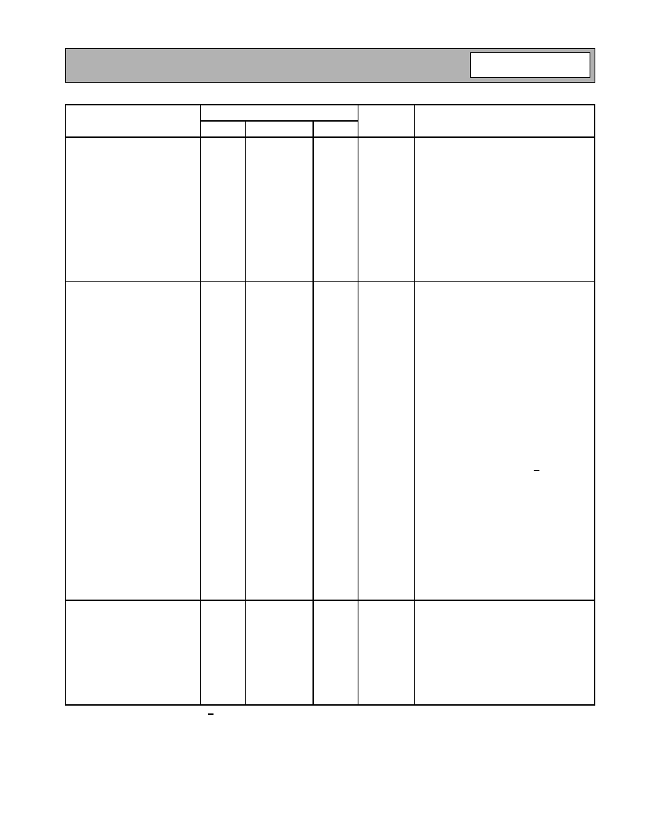
VCC OUT
DCS/PCS OUT
VCC
2
DCS/PCS IN
BAND SELECT
VREG
VRAMP
TX ENABLE
VBATT
GSM OUT
VCC
2
GSM IN
10
11
12
1
3
2
6
5
4
9
8
7
RF3110
TRIPLE-BAND GSM/DCS/PCS
POWER AMP MODULE
∑ 3V Dual-Band GSM Handsets
∑ Commercial and Consumer Systems
∑ Portable Battery-Powered Equipment
∑ GSM, E-GSM and DCS/PCS Products
∑ GPRS Class 12 Compatible
The RF3110 is a high-power, high-efficiency power ampli-
fier module with integrated power control. The device is
self-contained with 50
input and output terminals. The
power control function is also incorporated, eliminating
the need for directional couplers, detector diodes, power
control ASICs and other power control circuitry; this
allows the module to be driven directly from the DAC out-
put. The device is designed for use as the final RF ampli-
fier in GSM/DCS and PCS handheld digital cellular
equipment and other applications in the 880MHz to
915MHz, 1710MHz to 1785MHz and 1850MHz to
1910MHz bands. On-board power control provides over
35dB of control range with an analog voltage input; and,
power down with a logic "low" for standby operation.
∑ Complete Power Control Solution
∑ Single 3.0V to 5.5V Supply Voltage
∑ +35dBm GSM Output Power at 3.5V
∑ +33dBm DCS/PCS Output Power at 3.5V
∑ 55% GSM and 55% DCS/PCS
EFF
∑ 10mmx10mm Package Size
RF3110
Triple-Band GSM/DCS/PCS Power Amp Module
RF3110 PCBA
Fully Assembled Evaluation Board
RF3110 DBP
Power Amplifier Module, 5 Piece Sample Pack
0
Rev A7 021213
1.70
1.45
0.450
± 0.075
0.
40
0 T
Y
P
1.
20
0 T
Y
P
1.
80
0 T
Y
P
2.
60
0 T
Y
P
3.
20
0 T
Y
P
4.
00
0 T
Y
P
4.
60
0 T
Y
P
5.
40
0 T
Y
P
6.
00
0 T
Y
P
6.
80
0 T
Y
P
7.
40
0 T
Y
P
8.
20
0 T
Y
P
8.
27
5 T
Y
P
8.
80
0 T
Y
P
9.
60
0 T
Y
P
9.600 TYP
8.800 TYP
8.200 TYP
7.400 TYP
6.800 TYP
6.000 TYP
5.400 TYP
4.600 TYP
4.000 TYP
3.200 TYP
2.600 TYP
1.800 TYP
1.200 TYP
0.400 TYP
0.000
9.
0
98 TYP
0.
000
1.
797
8.
205
8.
280
1.245
4.075
5.925
8.747
0.306
Pin 1
10.00 ± 0.10
Pin 1
10.00 ± 0.10
Top View
Bottom View
Package Style: Module
!
!

2-402
RF3110
Rev A7 021213
Absolute Maximum Ratings
Parameter
Rating
Unit
Supply Voltage
-0.3 to +6.0
V
DC
Power Control Voltage (V
RAMP
)
-0.3 to +1.8
V
Input RF Power
+11.5
dBm
Max Duty Cycle
50
%
Output Load VSWR
10:1
Operating Case Temperature
-20 to +85
∞C
Storage Temperature
-55 to +150
∞C
Parameter
Specification
Unit
Condition
Min.
Typ.
Max.
Overall (GSM Mode)
Temp=+25 ∞C, V
BATT
=3.5V, V
RAMP
=V
RAMP
Max, P
IN
=6dBm, Freq=880MHz to
915MHz, 25% Duty Cycle, Pulse
Width=1154
µ
s
Operating Frequency Range
880 to 915
MHz
Maximum Output Power
+34.5
35.0
dBm
Temp = 25∞C, V
BATT
=3.5V,
V
RAMP
=V
RAMP
Max
+32.0
dBm
Temp=+85∞C, V
BATT
=3.0V,
V
RAMP
=V
RAMP
Max
Total Efficiency
47
53
%
At P
OUT
,
MAX
, V
BATT
=3.5V
Input Power Range
+4
+6
+8
dBm
Full output power guaranteed at minimum
drive level
Output Noise Power
-86
-80
dBm
RBW=100kHz, 925MHz to 935MHz,
P
OUT
> +5dBm
-88
-85
dBm
RBW=100kHz, 935MHz to 960MHz,
P
OUT
> +5dBm
Forward Isolation
-31.5
-25
dBm
TX_ENABLE=0V, PIN=+8dBm
Second Harmonic
-15
-7
dBm
Over all power levels
Third Harmonic
-15
-7
dBm
Over all power levels
All other Non-Harmonic Spurious
-36
dBm
Over all power levels
Crossband Isolation (2f
0
)
-20
dBm
Input Impedance
50
Input VSWR
2.5:1
Over all power levels
Output Load VSWR
8:1
Spurious<-36dBm, V
RAMP
=0.2V to 1.6V,
RBW=3MHz
Output Load VSWR Ruggedness
10:1
Output Load Impedance
50
Load impedance presented at RF OUT pad
Power Control V
RAMP
Power Control "ON"
1.6
V
Max. P
OUT
, Voltage supplied to the input
Power Control "OFF"
0.2
0.25
V
Min. P
OUT
, Voltage supplied to the input
Power Control Range
35
dB
V
RAMP
=0.2V to 1.6V
V
RAMP
Input Capacitance
15
pF
DC to 2MHz
V
RAMP
Input Current
10
µ
A
V
RAMP
=1.6V
Turn On/Off Time
4
µ
S
V
RAMP
=0 to 1.6V
Note: V
RAMP
Max=3/8*V
BATT
+0.18<1.6V
Caution! ESD sensitive device.
RF Micro Devices believes the furnished information is correct and accurate
at the time of this printing. However, RF Micro Devices reserves the right to
make changes to its products without notice. RF Micro Devices does not
assume responsibility for the use of the described product(s).
2-403
RF3110
Rev A7 021213
Parameter
Specification
Unit
Condition
Min.
Typ.
Max.
Overall Power Supply
Power Supply Voltage
3.5
V
Specifications
3.0
5.5
V
Nominal operating limits, P
OUT
<+35dBm
3.0
4.3
V
50% Duty Cycle, Pulse width 2308
µ
s
V
RAMP
0.2
1.6
V
0.2
1.336
V
50% Duty Cycle, Pulse width 2308
µ
s
Power Supply Current
2
A
DC Current at P
OUT,MAX
1
10
µ
A
P
IN
<-30dBm, V
RAMP
=0V,
Temp=-40∞C to +85∞C
V
REG
Voltage
2.7
2.8
2.9
V
V
REG
Current
7
mA
TX Enable=High
10
µ
A
TX Enable=Low
Overall (DCS/PCS Mode)
Temp=25∞C, V
BATT
=3.5V, V
RAMP
=V
RAMP
Max, P
IN
=6dBm, Freq=1710MHz to
1785MHz, 25% Duty Cycle, pulse
width=1154
µ
s
Operating Frequency Range
1710 to 1910
MHz
Maximum Output Power
+32
+33
dBm
Temp=25∞C, V
BATT
=3.5V, V
RAMP
=V
RAMP
Max, 1710MHz to 1785MHz
31.5
32.5
dBm
1850-1910MHz
30
dBm
Temp=+85∞C, V
BATT
=3.0V, V
RAMP
= V
RAMP
Max, 1710MHz to 1785MHz
29.5
dBm
1850MHz to 1910MHz
Total Efficiency
47
52
%
At P
OUT,MAX,
V
BATT
=3.5V, 1710-1785MHz
45
1850-1910MHz
Input Power Range
+4
+6
+8
dBm
Full output power guaranteed at minimum
drive level
Output Noise Power
-77
dBm
RBW=100kHz, 1805MHz to 1880MHz and
1930MHz to 1990MHz, P
OUT
> 0dBm,
V
BATT
=3.5V
Forward Isolation
-37
-30
dBm
TX_ENABLE=0V, P
IN
=+8dBm
Second Harmonic
-25
-13
dBm
Over all power levels
Third Harmonic
-30
-15
dBm
Over all power levels
All other Non-Harmonic Spurious
-36
dBm
Over all power levels
Input Impedance
50
Input VSWR
-
2.5
Over all power levels
Output Load VSWR
8:1
Spurious<-36dBm, V
APCDCS
=0.2V to 1.5V,
RBW=3MHz
Output Load VSWR Ruggedness
10:1
Output Load Impedance
50
Load impedance presented at RF OUT pin
Power Control V
RAMP
Power Control "ON"
1.6
V
Max. P
OUT
, Voltage supplied to the input
Power Control "OFF"
0.2
0.25
V
Min. P
OUT
, Voltage supplied to the input
Power Control Range
33
dB
V
RAMP
=0.2V to 1.6V, P
IN
=+8dBm
V
RAMP
Input Capacitance
15
pF
DC to 2MHz
V
RAMP
Input Current
10
µ
A
V
RAMP
=1.6V
10
µ
A
V
RAMP
=0V
Turn On/Off Time
4
µ
s
V
RAMP
=0to1.6V
Note: V
RAMP
max=3/8*V
BATT
+0.18<1.6V

2-404
RF3110
Rev A7 021213
Parameter
Specification
Unit
Condition
Min.
Typ.
Max.
Overall Power Supply
Power Supply Voltage
3.5
V
Specifications
3.0
5.5
V
Nominal operating limits, P
OUT
<+33dBm
3.0
4.3
V
50% Duty Cycle, Pulse width 2308
µ
s
V
RAMP
0.2
1.6
V
0.2
1.263
V
50% Duty Cycle, Pulse width 2308
µ
s
Power Supply Current
1
10
µ
A
P
IN
<-30dBm, V
RAMP
=0V,
Temp=-20∞C to +85∞C
V
REG
Voltage
2.7
2.8
2.9
V
V
REG
Current
7
8
mA
TX Enable=High
10
µ
A
TX Enable=Low
2-405
RF3110
Rev A7 021213
Pin
Function
Description
Interface Schematic
1
DCS/PCS IN
RF input to the DCS band. This is a 50
input.
2
BAND
SELECT
Allows external control to select the GSM or DCS band with a logic high
or low. A logic low enables the GSM band whereas a logic high enables
the DCS band.
3
TX ENABLE
This signal enables the PA module for operation with a logic high. Once
TX Enable is asserted the RF output level will increase to 0dBm.
4
VBATT
Power supply for the module. This should be connected to the battery.
5
VREG
Regulated voltage input for power control function. (2.8V nom)
6
VRAMP
Ramping signal from DAC. A simple RC filter may need to be con-
nected between the DAC output and the VRAMP input depending on
the baseband selected. The ramping profiles shown later in the data
sheet are recommended profiles for meeting the GSM specification for
burst timing and transient spectrum.
7
GSM IN
RF input to the GSM band. This is a 50
input.
8
VCC2
Controlled voltage input to driver stage for GSM bands. This voltage is
part of the power control function for the module. This node must be
connected to V
CC
out.
9
GSM OUT
RF output for the GSM band. This is a 50
output. The output load line
matching is contained internal to the package.
10
VCC OUT
Controlled voltage output to feed V
CC2
. This voltage is part of the
power control function for the module. It can not be connected to any-
thing other than V
CC2
, nor can any component be placed on this node
(i.e. decoupling capacitor).
11
DCS/PCS
OUT
RF output for the DCS band. This is a 50
output. The output load line
matching is contained internal to the package.
12
VCC2
Controlled voltage input to DCS driver stage. This voltage is part of the
power control function for the module. This node must be connected to
V
CC
out
Pkg
Base
GND