 | –≠–ª–µ–∫—Ç—Ä–æ–Ω–Ω—ã–π –∫–æ–º–ø–æ–Ω–µ–Ω—Ç: RF3146 | –°–∫–∞—á–∞—Ç—å:  PDF PDF  ZIP ZIP |

2-491
Product Description
Ordering Information
Typical Applications
Features
Functional Block Diagram
RF Micro Devices, Inc.
7628 Thorndike Road
Greensboro, NC 27409, USA
Tel (336) 664 1233
Fax (336) 664 0454
http://www.rfmd.com
Optimum Technology MatchingÆ Applied
Si BJT
GaAs MESFET
GaAs HBT
Si Bi-CMOS
SiGe HBT
Si CMOS
InGaP/HBT
GaN HEMT
SiGe Bi-CMOS
DCS/PCS IN
DCS/PCS OUT
BAND SELECT
TX ENABLE
VRAMP
VBATT
GSM IN
GSM OUT
VBATT
37
40
41
45
42
48
31
6
43
Fully Integrated
Power Control Circuit
RF3146
QUAD-BAND GSM850/GSM900/DCS/PCS
POWER AMP MODULE
∑ 3V Quad-Band GSM Handsets
∑ Commercial and Consumer Systems
∑ Portable Battery-Powered Equipment
∑ GSM850/EGSM900/DCS/PCS Products
∑ GPRS Class 12 Compatible
∑ Power Star
TM
Module
The RF3146 is a high-power, high-efficiency power ampli-
fier module with integrated power control. The device is a
self-contained 7mmx7mmx0.9mm lead frame module
(LFM) with 50
input and output terminals. The power
control function is also incorporated, eliminating the need
for directional couplers, detector diodes, power control
ASICs and other power control circuitry; this allows the
module to be driven directly from the DAC output. The
device is designed for use as the final RF amplifier in
GSM850, EGSM900, DCS and PCS handheld digital cel-
lular equipment and other applications in the 824MHz to
849MHz, 880MHz to 915MHz, 1710MHz to 1785MHz
and 1850MHz to 1910MHz bands. On-board power con-
trol provides over 50dB of control range with an analog
voltage input; and, power down with a logic "low" for
standby operation.
∑ Integrated V
REG
∑ Complete Power Control Solution
∑ +35dBm GSM Output Power at 3.5V
∑ +33dBm DCS/PCS Output Power at 3.5V
∑ 60% GSM and 55% DCS/PCS
EFF
∑ 7mmx7mmx0.9mm Package Size
RF3146
Quad-Band GSM850/GSM900/DCS/PCS Power
Amp Module
RF3146 SB
Power Amp Module 5-Piece Sample Pack
RF3146 PCBA
Fully Assembled Evaluation Board
0
Rev A7 040812 W3
Dimensions in mm.
Shaded lead is pin 1.
-B-
2 PLCS
0.10 C B
2 PLCS
0.10 C A
2 PLCS
0.10 C B
3.50 TYP
3.37 TYP
-A-
2 PLCS
0.10 C A
7.00 TYP
6.75 TYP
0.70
0.65
0.90
0.85
0.08 C
0.05
0.00
SEATING
PLANE
-C-
0.10 C A B
M
2.20
1.90
5.25
4.95
0.50
0.30
TYP
0.30
0.60
0.24
TYP
0.60
0.24
TYP
0.30
0.18
0.50
Package Style: LFM, 48-Pin, 7mm x7mmx0.9mm
Preliminary

Preliminary
2-492
RF3146
Rev A7 040812 W3
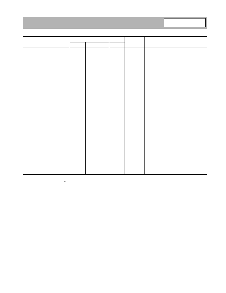
Absolute Maximum Ratings
Parameter
Rating
Unit
Supply Voltage
-0.3 to +6.0
V
DC
Power Control Voltage (V
RAMP
)
-0.3 to +1.8
V
Input RF Power
+10
dBm
Max Duty Cycle
50
%
Output Load VSWR
10:1
Operating Case Temperature
-20 to +85
∞C
Storage Temperature
-55 to +150
∞C
Parameter
Specification
Unit
Condition
Min.
Typ.
Max.
Overall Power Control
V
RAMP
Power Control "ON"
1.5
V
Max. P
OUT
, Voltage supplied to the input
Power Control "OFF"
0.2
0.25
V
Min. P
OUT
, Voltage supplied to the input
V
RAMP
Input Capacitance
15
20
pF
DC to 2MHz
V
RAMP
Input Current
10
µ
A
V
RAMP
=V
RAMP MAX
Turn On/Off Time
2
µ
s
V
RAMP
=0.2V to V
RAMP MAX
TX Enable "ON"
1.9
V
TX Enable "OFF"
0.5
V
GSM Band Enable
0.5
V
DCS/PCS Band Enable
1.9
V
Overall Power Supply
Power Supply Voltage
3.5
V
Specifications
V
Nominal operating limits
Power Supply Current
1
µ
A
P
IN
<-30dBm, TX Enable=Low,
Temp=-20∞C to +85∞C
mA
V
RAMP
=0.2V, TX Enable=High
Overall Control Signals
Band Select "Low"
0
0
0.5
V
Band Select "High"
1.9
2.0
3.0
V
Band Select "High" Current
20
50
µ
A
TX Enable "Low"
0
0
0.5
V
TX Enable "High"
1.9
2.0
3.0
V
TX Enable "High" Current
1
2
µ
A
Caution! ESD sensitive device.
RF Micro Devices believes the furnished information is correct and accurate
at the time of this printing. However, RF Micro Devices reserves the right to
make changes to its products without notice. RF Micro Devices does not
assume responsibility for the use of the described product(s).

Preliminary
2-493
RF3146
Rev A7 040812 W3
Parameter
Specification
Unit
Condition
Min.
Typ.
Max.
Overall (GSM850 Mode)
Temp=+25 ∞C, V
BATT
=3.5V,
V
RAMP
=V
RAMP MAX
, P
IN
=3dBm,
Freq=824MHz to 849MHz,
25% Duty Cycle, Pulse Width=1154
µ
s
Operating Frequency Range
824 to 849
MHz
Maximum Output Power
+34.2
dBm
Temp = 25∞C, V
BATT
=3.5V,
V
RAMP
=V
RAMP MAX
+32.0
dBm
Temp=+85 ∞C, V
BATT
=3.0V,
V
RAMP
=V
RAMP MAX
Total Efficiency
47
55
%
At P
OUT
MAX
, V
BATT
=3.5V
Input Power Range
0
+3
+5
dBm
Maximum output power guaranteed at mini-
mum drive level
Output Noise Power
-88
-81
dBm
RBW=100kHz, 869MHz to 894MHz,
P
OUT
> +5dBm
Forward Isolation 1
-50
-35
dBm
TXEnable=Low, P
IN
=+5dBm
Forward Isolation 2
-35
-15
dBm
TXEnable=High, P
IN
=+5dBm, V
RAMP
=0.2V
Cross Band Isolation at 2f
0
-18
dBm
V
RAMP
=0.2V to V
RAMP
_R
P
Second Harmonic
-15
-7
dBm
V
RAMP
=0.2V to V
RAMP
_R
P
Third Harmonic
-25
-15
dBm
V
RAMP
=0.2V to V
RAMP
_R
P
All Other
Non-Harmonic Spurious
-36
dBm
V
RAMP
=0.2V to V
RAMP MAX
Input Impedance
50
Input VSWR
2.5:1
V
RAMP
=0.2V to V
RAMP MAX
Output Load VSWR Stability
8:1
Spurious<-36dBm, RBW=3MHz
Set V
RAMP
where P
OUT
<34.2dBm into 50
load
Output Load VSWR Ruggedness
10:1
Set V
RAMP
where P
OUT
<34.2dBm into 50
load. No damage or permanent degradation
to part.
Output Load Impedance
50
Load impedance presented at RF OUT pad
Power Control V
RAMP
Power Control Range
55
dB
V
RAMP
=0.2V to V
RAMP MAX
Notes:
V
RAMP MAX
=0.4*V
BATT
+0.06<1.5V
V
RAMP
_R
P
=V
RAMP
set for 34.2dBm at nominal conditions.

Preliminary
2-494
RF3146
Rev A7 040812 W3
Parameter
Specification
Unit
Condition
Min.
Typ.
Max.
Overall (GSM900 Mode)
Temp=+25 ∞C, V
BATT
=3.5V,
V
RAMP
=V
RAMP MAX
, P
IN
=3dBm,
Freq=880MHz to 915MHz,
25% Duty Cycle, Pulse Width=1154
µ
s
Operating Frequency Range
880 to 915
MHz
Maximum Output Power
+34.2
dBm
Temp = 25∞C, V
BATT
=3.5V,
V
RAMP
=V
RAMP MAX
+32.0
dBm
Temp=+85 ∞C, V
BATT
=3.0V,
V
RAMP
=V
RAMP MAX
Total Efficiency
54
58
%
At P
OUT
MAX
, V
BATT
=3.5V
Input Power Range
0
+3
+5
dBm
Maximum output power guaranteed at mini-
mum drive level
Output Noise Power
-86
-80
dBm
RBW=100kHz, 925MHz to 935MHz,
P
OUT
> +5dBm
-88
-84
dBm
RBW=100kHz, 935MHz to 960MHz,
P
OUT
> +5dBm
Forward Isolation 1
-45
-35
dBm
TXEnable=Low, P
IN
=+5dBm
Forward Isolation 2
-30
-15
dBm
TXEnable=High, V
RAMP
=0.2V, P
IN
=+5dBm
Cross Band Isolation 2f
0
-17
dBm
V
RAMP
=0.2V to V
RAMP
_R
P
Second Harmonic
-15
-10
dBm
V
RAMP
=0.2V to V
RAMP
_R
P
Third Harmonic
-25
-15
dBm
V
RAMP
=0.2V to V
RAMP
_R
P
All Other
Non-Harmonic Spurious
-36
dBm
V
RAMP
=0.2V to V
RAMP MAX
Input Impedance
50
Input VSWR
2.5:1
V
RAMP
=0.2V to V
RAMP MAX
Output Load VSWR Stability
8:1
Spurious<-36dBm, RBW=3MHz
Set V
RAMP
where P
OUT
<34.2dBm into 50
load
Output Load VSWR Ruggedness
10:1
Set V
RAMP
where P
OUT
<34.2dBm into 50
load. No damage or permanent degradation
to part.
Output Load Impedance
50
Load impedance presented at RF OUT pad
Power Control V
RAMP
Power Control Range
50
dB
V
RAMP
=0.2V to V
RAMP MAX
Notes:
V
RAMP MAX
=0.4*V
BATT
+0.06<1.5V
V
RAMP
_R
P
=V
RAMP
set for 34.2dBm at nominal conditions.
Preliminary
2-495
RF3146
Rev A7 040812 W3
Parameter
Specification
Unit
Condition
Min.
Typ.
Max.
Overall (DCS Mode)
Temp=25∞C, V
BATT
=3.5V,
V
RAMP
=V
RAMP MAX
, P
IN
=3dBm,
Freq=1710MHz to 1785MHz,
25% Duty Cycle, pulse width=1154
µ
s
Operating Frequency Range
1710 to 1785
MHz
Maximum Output Power
+32.0
dBm
Temp=25∞C, V
BATT
=3.5V,
V
RAMP
=V
RAMP MAX
30
dBm
Temp=+85∞C, V
BATT
=3.0V,
V
RAMP
=V
RAMP MAX
Total Efficiency
45
52
%
At P
OUT MAX,
V
BATT
=3.5V
Input Power Range
0
+3
+5
dBm
Maximum output power guaranteed at mini-
mum drive level
Output Noise Power
-85
-80
dBm
RBW=100kHz, 1805MHz to 1880MHz,
P
OUT
> 0dBm,
V
BATT
=3.5V
Forward Isolation 1
-50
-35
dBm
TXEnable=Low, P
IN
=+5dBm
Forward Isolation 2
-25
-15
dBm
TXEnable=High, V
RAMP
=0.2V, P
IN
=+5dBm
Second Harmonic
-15
-7
dBm
V
RAMP
=0.2V to V
RAMP
_R
P
Third Harmonic
-20
-15
dBm
V
RAMP
=0.2V to V
RAMP
_R
P
All Other
Non-Harmonic Spurious
-36
dBm
V
RAMP
=0.2V to V
RAMP MAX
Input Impedance
50
Input VSWR
2.5:1
V
RAMP
=0.2V to V
RAMP MAX
Output Load VSWR Stability
8:1
Spurious<-36dBm, RBW=3MHz
Set V
RAMP
where P
OUT
<32.0dBm into 50
load
Output Load VSWR Ruggedness
10:1
Set V
RAMP
where P
OUT
<32.0dBm into 50
load. No damage or permanent degradation
to part.
Output Load Impedance
50
Load impedance presented at RF OUT pin
Power Control V
RAMP
Power Control Range
50
dB
V
RAMP
=0.2V to V
RAMP MAX
, P
IN
=+5dBm
Notes:
V
RAMP MAX
=0.4*V
BATT
+0.06<1.5V
V
RAMP
_R
P
=V
RAMP
set for 32.0dBm at nominal conditions.