
¸
2-261
2
PO
W
E
R
A
M
P
LI
FI
E
R
S
Preliminary
Product Description
Ordering Information
Typical Applications
Features
Functional Block Diagram
RF Micro Devices, Inc.
7625 Thorndike Road
Greensboro, NC 27409, USA
Tel (336) 664 1233
Fax (336) 664 0454
http://www.rfmd.com
Optimum Technology MatchingÆ Applied
Si BJT
GaAs MESFET
GaAs HBT
Si Bi-CMOS
SiGe HBT
Si CMOS
¸
DCS IN
V
APC
GSM IN
GND
DCS OUT
GSM OUT
GND
13
11
12
9
10
1
2
4
3
5
VC
C
8
GND
7
VC
C
6
14
GN
D
15
BAN
D
S
E
L
EC
T
16
GND
GND
GND
GND
RF3160
DUAL-BAND GSM/DCS
POWER AMP MODULE
∑ 3V Dual-Band GSM/DCS Handsets
∑ Commercial and Consumer Systems
∑ Portable Battery-Powered Equipment
∑ GPRS Compatible
∑ GSM, E-GSM and DCS Products
The RF3160 is a high-power, high-efficiency power ampli-
fier module. The device is self-contained with 50
input
and output terminals. The device is manufactured on an
advanced Gallium Arsenide Heterojunction Bipolar Tran-
sistor (HBT) process, and has been designed for use as
the final RF amplifier in GSM/DCS handheld digital cellu-
lar equipment and other applications in the 880MHz to
915MHz and 1710MHz to 1785MHz bands. On-board
power control provides over 70dB of control range with an
analog voltage input, and provides power down with a
logic "low" for standby operation. The device is packaged
in an ultra-small (9mmx11mm) LCC, minimizing the
required board space.
∑ Single 2.8V to 5.0V Supply Voltage
∑ +35.0dBm GSM Output Power at 3.2V
∑ +32.5dBm DCS Output Power at 3.2V
∑ 55% GSM and 50% DCS Efficiency
∑ Internal Band Select
RF3160
Dual-Band GSM/DCS Power Amp Module
RF3160 PCBA
Fully Assembled Evaluation Board
2
Rev A4 010420
Side View
Dimensions in mm.
All contact points are gold-plated,
lead-free surfaces.
9.09
±0.10
0.450
±0.075
1.40
1.25
1
0.760
TYP
4.520
0.920
TYP
1.910
TYP
FULL
RADIUS
TYP
R0.860
TYP
7.040
2. All dimensions without specific tolerances are for reference only.
NOTES:
1. Shaded area is pin 1.
Bottom View
11.61
± 0.10
Package Style: Module (9mmx11mm)

Preliminary
2-262
RF3160
Rev A4 010420
2
PO
W
E
R
A
M
P
LI
FI
E
R
S
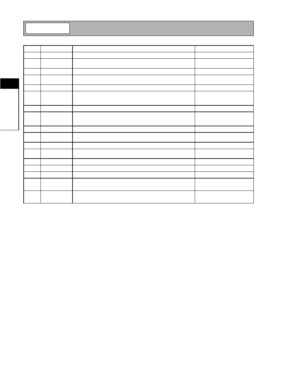
Absolute Maximum Ratings
Parameter
Rating
Unit
Supply Voltage
-0.5 to +5.0
V
DC
Power Control Voltage (V
APC1,2
)
-0.5 to +3.0
V
DC Supply Current
2400
mA
Input RF Power
+15
dBm
Duty Cycle at Max Power
50
%
Output Load VSWR
6:1
Operating Case Temperature
-30 to +85
∞C
Storage Temperature
-30 to +85
∞C
Parameter
Specification
Unit
Condition
Min.
Typ.
Max.
Overall (GSM Mode)
Temp= +25∞C, V
CC
= 3.2V, V
APC GSM
= 1.9V,
P
IN
=6dBm, Freq= 880MHz to 915MHz,
25% Duty Cycle, Pulse Width= 1154
µ
s
Operating Frequency Range
880 to 915
MHz
Maximum Output Power
34.5
35.0
dBm
Temp = 25∞C, V
CC
= 3.2V, V
APCGSM
=1.9V
PAE Efficiency
50
55
%
At P
OUT
,
MAX
, V
CC
= 3.2V
Input Power for Max Output
+6
+8
+10
dBm
Output Noise Power
-72
dBm
RBW= 100kHz, 925MHz to 935MHz,
P
OUT
>34.5dBm
-84
dBm
RBW= 100kHz, 935MHz to 960MHz,
P
OUT
>34.5dBm
Forward Isolation
-40
dBm
V
APCGSM
=0.1V, P
IN
=-5dBm
Cross-Band Isolation
-15
dBm
P
OUT
>34.5dBm
Second Harmonic
-7
dBm
5dBm < P
OUT
<34.5dBm
Third Harmonic
-7
dBm
All Other Non-Harmonic
Spurious
-7
dBm
Input Impedance
50
Input VSWR
3:1
Output Load VSWR (Stability)
6:1
Spurious<-36dBm, V
APCGSM
= 0.1V to 1.9V,
RBW= 3MHz
Output Load VSWR (Rugged-
ness)
10:1
P
IN
=6dBm, P
OUT
<34.5dBm,
V
CC
= 4.6V, Z
S
= 50
Output Load Impedance
50
Load impedance presented at RF OUT pad
Power Control V
APC1
Power Control "ON"
1.8
1.9
V
Max. P
OUT
Power Control "OFF"
0.1
0.5
V
Min. P
OUT
Power Control Range
60
dB
V
APC1,2
= 0.1V to 1.9V
Gain Control Slope
100
dB/V
P
OUT
=-10dBm to 34.5dBm
APC Input Capacitance
10
pF
DC to 2MHz
APC Input Current
1
mA
V
APC
= 1.9V
10
µ
A
V
APC
=0V
Turn On/Off Time
2
µ
S
V
APC
=0V to 1.9V
Band Select
0
0.5
V
GSM
2
2.8
V
DCS
Overall Power Supply
Power Supply Voltage
2.8
3.2
5.0
V
Specifications
2.9
4.7
V
Nominal operating limits, P
OUT
<+34.5dBm
Power Supply Current
2
A
DC Current at P
OUT,MAX
30
µ
A
V
APC1,2
=0.1V. No RF input power.
Caution! ESD sensitive device.
RF Micro Devices believes the furnished information is correct and accurate
at the time of this printing. However, RF Micro Devices reserves the right to
make changes to its products without notice. RF Micro Devices does not
assume responsibility for the use of the described product(s).

Preliminary
2-263
RF3160
Rev A4 010420
2
PO
W
E
R
A
M
P
LI
FI
E
R
S
Parameter
Specification
Unit
Condition
Min.
Typ.
Max.
Overall (DCS Mode)
Temp= 25∞C, V
CC
= 3.2V,
V
APCDCS
= 1.9V, P
IN
=6dBm,
Freq= 1710MHz to 1785MHz,
25% Duty Cycle, pulse width= 1154
µ
s
Operating Frequency Range
1710 to 1785
MHz
Maximum Output Power
31.9
32.5
dBm
Temp= 25∞C, V
CC
= 3.2V,
V
APCDCS
= 1.9V, 1710MHz to 1785MHz
PAE Efficiency
42
50
%
At P
OUT,MAX,
V
CC
= 3.2V,
1710MHz to 1785MHz
Recommended Input Power
Range
+6
+8
+10
dBm
Output Noise Power
-80
-76
dBm
RBW =100kHz, 1805MHz to 1880MHz,
P
OUT
> 32.5dBm, V
CC
= 3.2V
Forward Isolation
-48
dBm
V
APCDCS
= 0.1V, P
IN
=-5dBm
Second Harmonic
-7
dBm
0dBm <P
OUT
<32.5dBm
Third Harmonic
-7
dBm
All Other Non-Harmonic
Spurious
-7
dBm
Input Impedance
50
Input VSWR
3:1
Output Load VSWR (Stability)
6:1
Spurious <-36dBm,
V
APCDCS
=0.1V to 1.9V, RBW = 3MHz
Output Load VSWR (Rugged-
ness)
10:1
P
IN
=6dBm, P
OUT
<31.9dBm,
V
CC
= 4.6V, Z
S
= 50
Output Load Impedance
50
Load impedance presented at RF OUT pin
Power Control V
APC 2
Power Control "ON"
1.8
1.9
V
Max. P
OUT
Power Control "OFF"
0.1
0.5
V
Min. P
OUT
Power Control Range
60
dB
V
APC1,2
= 0.1V to 1.9V
Gain Control Slope
100
dB/V
P
OUT
= -10dBm to +32.5dBm
APC Input Capacitance
10
pF
DC to 2MHz
APC Input Current
1
mA
V
APC
= 1.9V
10
µ
A
V
APC
=0V
Turn On/Off TIme
100
ns
V
APC
=0to1.9V
Overall Power Supply
Power Supply Voltage
3.2
V
Specifications
2.9
4.7
V
Nominal operating limits, P
OUT
<+32.5dBm
Power Supply Current
1.3
A
DC Current at P
OUT,MAX
30
µ
A
V
APC1,2
=0.1V. No RF input power.
Preliminary
2-264
RF3160
Rev A4 010420
2
PO
W
E
R
A
M
P
LI
FI
E
R
S
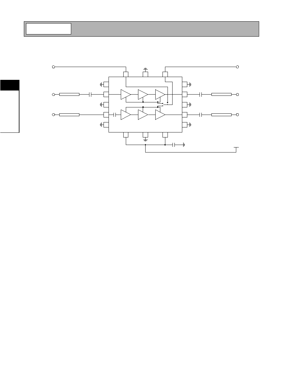
Pin
Function
Description
Interface Schematic
1
GND
Connects to module backside ground.
2
DCS IN
RF input to the DCS band. This is a 50
input, external DC-blocking
capacitor required. See application schematic.
3
GND
Connects to module backside ground.
4
GSM IN
RF input to the GSM band. This is a 50
input. No external DC-block-
ing capacitor required. See application schematic.
5
GND
Connects to module backside ground.
6
VCC
Power supply for stages 1 and 2 of both the GSM and DCS power
amplifiers. External low frequency bypassing capacitor required. See
application schematic.
7
GND
Connects to module backside ground.
8
VCC
Power supply for output stages of both the GSM and DCS power ampli-
fiers. External low frequency bypassing capacitor required. See appli-
cation schematic.
9
GND
Connects to module backside ground.
10
GSM OUT
RF output for the GSM band. This is a 50
output. External DC-block-
ing capacitor required. See application schematic.
11
GND
Connects to module backside ground.
12
DCS OUT
RF output for the DCS band. This is a 50
output. External DC-block-
ing capacitor required. See application schematic.
13
GND
Connects to module backside ground.
14
VAPC
Single input analog power control voltage for the GSM and DCS band.
15
GND
Connects to module backside ground.
16
BAND
SELECT
Logic low (GSM enable) or logic high (DCS enable) provides single IO
band selection.
Pkg
Base
GND
Module backside ground.

Preliminary
2-265
RF3160
Rev A4 010420
2
PO
W
E
R
A
M
P
LI
FI
E
R
S
Pin Out
Top View
GND
DCS IN
GND
GSM IN
GND
GN
D
VC
C
VC
C
GND
GND
GND
GN
D
GSM OUT
DCS OUT
V
AP
C
BA
ND
S
E
L
EC
T
13
12
11
10
9
14
15
16
8
7
6
1
2
3
4
5
Preliminary
2-266
RF3160
Rev A4 010420
2
PO
W
E
R
A
M
P
LI
FI
E
R
S
Application Schematic
50
µ
strip
50
µ
strip
50
µ
strip
50
µ
strip
GSM IN
DCS IN
13
11
12
9
10
1
2
4
3
5
8
7
6
14
15
16
VAPC
BAND SELECT
V
CC
DCS OUT
GSM OUT
10 pF
33 pF
10 pF
3.3 uF

Preliminary
2-267
RF3160
Rev A4 010420
2
PO
W
E
R
A
M
P
LI
FI
E
R
S
Evaluation Board Layout
Board Size 2.0" x 2.0"
Board Thickness 0.032", Board Material FR-4, Multi-Layer
Assembly
Top
Inner 1
Back

Preliminary
2-268
RF3160
Rev A4 010420
2
PO
W
E
R
A
M
P
LI
FI
E
R
S