 | –≠–ª–µ–∫—Ç—Ä–æ–Ω–Ω—ã–π –∫–æ–º–ø–æ–Ω–µ–Ω—Ç: SIW1711 | –°–∫–∞—á–∞—Ç—å:  PDF PDF  ZIP ZIP |
Document Outline
- Description
- Pin Description
- Table 1. SiW1711 Radio Modem Pin List
- System Specifications
- Absolute Maximum Ratings
- Recommended Operating Conditions
- ESD Rating
- Electrical Characteristics
- DC Specification (TOP = +25�C, VDD_IO = 3.0 V)
- AC Characteristics (TOP = +25�C, VDD_IO = 3.0 V, CLOAD = 15 pF)
- Current Consumption (TOP = +25�C, VBATT_ANA, VBATT_DIG = 3.3 V)
- Digital Regulator Specification (TOP = 25�C)
- Internal Analog Voltage Regulator Specification (TOP = +25�C, VBATT_ANA = 3.3 V)
- Radio Specification
- RF Impedances
- Receiver Specification1 (VBATT_ANA, VBATT_DIG = 3.3 V, VCC = int. analog reg. output, and nominal2 Bluetooth test conditions)
- Transmitter Specification1 (VBATT_ANA, VBATT_DIG = 3.3 V, VCC = int. analog reg. output, and nominal Bluetooth test conditions)
- Industrial Temperature Performance1 (VBATT_ANA, VBATT_DIG = 3.3 V and extreme Bluetooth test conditions)
- External Reference Requirements
- Crystal Requirements
- Pin Assignments

1 of 12
RF Micro Devices, Inc.
7628 Thorndike Road
Greensboro, NC 27409, USA
Tel (336) 664 1233
Fax (336) 664 0454
http://www.rfmd.com
Features
Ordering Information
Product Description
Optimum Technology MatchingÆ Applied
Si BJT
Si Bi-CMOS
GaInP/HBT
GaAs HBT
SiGe HBT
GaN HEMT
GaAs MESFET
Si CMOS
SiGe Bi-CMOS
LNA
90
0
ADC
ADC
VCO/
PLL
DRIVER
90
0
DAC
DAC
PWR
CNTL
Serial Programming
Interface (SPI)
Register
File
Clock Generation and
Distribution
RF_IN
IDAC
RF_OUT
XTAL_P/CLK
XTAL_N
BB_CLK
SPI_SS
SPI_TXD
SPI_RXD
SPI_CLK
System
Control
Logic
RX_TX_DATA
CD_TXEN
ENABLE_RM
HOP_STROBE
RESET_N
TX_RX_SWITCH
Voltage Regulator and Power
Distribution
PLL
Control
GFSK
MODEM
Control
VR
EF
M
_
C
A
P
VR
EF
P
_
C
A
P
VT
U
N
E
CHG_P
UM
P
VBA
TT_A
N
A
VB
ATT_
D
I
G
VCC
_
OUT
VBB
_OUT
VDD_I
O
VBB
_RDY
The SiW1711TM Radio Modem is Silicon Wave's third-generation radio modem for
BluetoothÆ wireless communications and is based on 0.18µm CMOS technology. This
highly integrated transceiver was specifically designed to meet the rigorous RF perfor-
mance required for integrating Bluetooth into mobile phone applications.
The SiW1711 Radio Modem combines a 2.4GHz radio transceiver and Gaussian Fre-
quency Shift Keying (GFSK) modem with digital control functions. The IC also incorpo-
rates analog and digital voltage regulators, a reference Phase Lock Loop (PLL) to
enable multiple input frequencies, and a power-on-reset (POR) circuit.
The SiW1711 Radio Modem uses direct conversion (zero-IF) architecture. This allows
digital filtering for excellent interference rejection as compared to low IF solutions, and
also results in fewer spurious responses. The receiver has excellent sensitivity due to a
low noise RF design combined with an advanced modem design. A fast hardware AGC
enables full discovery of any device within the dynamic range of the receiver (solves
near-far issues). The transmitter can maintain a stable output power level up to +4dBm
for class 2 operation, which in combination with the excellent receiver performance
ensures the maximum possible range at the lowest system cost.
The device is available in a 32-pin QFN package with 5 x 5 x 1 mm dimensions. Known
good die with bumps is also available. Operating temperature range is guaranteed from
-40∞C to +85∞C with available extended high temperature range to 105∞C.
∑ Single chip IC with 2.4 GHz
transceiver and GFSK modem with
digital interface to external baseband
processor.
∑ Fully compliant with Bluetooth
specification 1.1 and 1.2.
∑ Supports multiple external reference
clocks or crystal frequencies with on-
chip reference PLL.
∑ Direct-conversion architecture with
no external channel filter or VCO
resonator components.
∑ Single-ended RX/TX pins reduce
system BOM cost by eliminating a
balun. On-chip RX/TX switching
eliminates external RX/TX switch.
∑ Typical -85 dBm receiver sensitivity
with excellent interference rejection
performance.
∑ Class 2 and 3 transmit output power
up to +4 dBm with output power
control loop for accurate power
control.
∑ Hardware AGC dynamically adjusts
receiver performance in changing
environments.
∑ Low out-of-band spurious emissions
prevents interference with mobile
phone frequencies.
∑ Option for Class 1 designs with
RX/TX switch control and multiple
modes of gain control.
∑ On-chip voltage regulation simplifies
voltage input requirement. Regulator
bypass mode enables use of external
regulator.
∑ 1.8 Volt analog and digital core
voltages; 1.63 Volt to 3.63 Volt
external I/O interface voltage.
∑ Low power consumption in active and
standby modes.
SiW1711
BluetoothÆ Radio Modem
0
60 0047 R00Grf SiW1711 Radio Modem IC DS
BLUETOOTHÆ RADIO
MODEM
SiW1711
September 30, 2004

2 of 12
SiW1711
60 0047 R00Grf SiW1711 Radio Modem IC DS
Description
The following figure shows the SiW1711 Radio Modem functional block diagram. During the receive process, the radio sig-
nal is taken from the single ended RF input pin that feeds into the low noise amplifier (LNA). The signal from the LNA is
directly down-converted to I/Q baseband, filtered with an anti-aliasing filter, and converted to digital with a high resolution
analog-to-digital converter. The critical channel filtering is done in the digital domain for stable and repeatable perfor-
mance. The signal is then processed by a high performance GFSK demodulator. The demodulator is programmable to
support baseband ICs from multiple OEMs. Within the demodulator, data detection and timing recovery circuits convert
the data for transfer to an external device. In addition, the IC has multiple internal self-calibration circuits to maintain stable
and repeatable performance from part-to-part as well as over the full temperature range.
The IC has two fully integrated regulators: one for the radio (analog regulator) and one for the digital logic (digital regula-
tor). The digital regulator can be used to supply a Bluetooth baseband controller.
Note: Both regulators can be bypassed if external regulation is desired. When bypassing the analog regulator, the
VBATT_ANA and VCC_OUT pins must be tied together and the external analog voltage (1.8 V) should be applied to the
VBATT_ANA pin. When bypassing the digital regulator, the VBATT_DIG pin should be left unconnected and the external
digital voltage (1.8 V) should be applied to VBB_OUT pin.
The IC also provides power on reset and glitch-free clock start-up. A reference PLL can be enabled to support a number of
different reference frequencies.
Digital control functions and a programming interface provide radio modem control and a flexible interface to external Blue-
tooth link controllers.
Radio Interface
The RF_IN and RF_OUT signals are combined using a simple matching circuit and then connected to a filter and the
antenna. The signals are single-ended to save the cost and space of a balun.
An internal power control loop maintains a very stable RF_OUT signal level over the full temperature range and from part
to part. This means predictable and repeatable range at any temperature.
For class 1 operation, the TX_RX_SWITCH and IDAC signals can be used to control a RX/TX switch and the gain of an
external PA. This interface is programmable. Features include control of signal polarity, 3 modes of gain control and full
programmability to linearize the PA gain control curve.
Modem Interface
The modem interface transfers the Bluetooth data between the SiW1711 Radio Modem and an external controller. For ref-
erence purposes, the pin description table provides a brief description of typical interface modes.
Clock Signals
Multiple reference clock frequencies (using either a crystal or an external reference source) can be used as a reference for
the RF circuits, to synthesize clocks for most of the internal digital circuits, and to supply external processors with timing
signals.
Serial Programming Interface (SPI)
The serial programming interface (SPI) is used to access the internal registers of the SiW1711 Radio Modem. The SPI is
a synchronous serial interface that can be clocked to speeds up to 8 MHz.
Host I/F
SPI
Modem I/F
& Data
Ext Power
Single-ended LNA
and Downconverter
Single-ended Driver
and Upconverter
ADC
DAC
Radio
Programming
and Control
GFSK
Demodulator
GFSK
Modulator
Reference
PLL
Modem
Clock
Generator
XTAL
Circuit
Analog
Regulator
Digital
Regulator
SiW1711 Radio Modem
SiW1750 or SiW1760
(or any compatible
Bluetooth controller)
Baseband
Bluetooth Subsystem Using the SiW1711 Radio Modem
Reference Clock
or
Crystal Input

3 of 12
SiW1711
60 0047 R00Grf SiW1711 Radio Modem IC DS
Power
The SiW1711 Radio Modem includes both analog and digital voltage regulators. Input options are based on factors such
as voltage source, where internal regulators are used, and I/O voltage.
Pin Description
The SiW1711 Radio Modem's radio and modem interface, the serial programming interface (SPI), and a single clock input
and supply voltage are required for proper operation. The following table provides detailed listings of pin descriptions
arranged by functional groupings.
Table 1. SiW1711 Radio Modem Pin List
Name
Pad Type
Description
Radio Interface Signal Description
RF_IN
Analog
RF signal input into the receiver.
RF_OUT
Analog
RF signal output from the transmitter.
IDAC
Analog
Power control to external power amplifier. This output provides a variable current source that
can be used to control the external power amp. Leave unconnected if not used.
TX_RX_SWITCH
CMOS output
Output signal to indicate the current state of the radio. The polarity is programmable with the
default set as:
Low=Transmit mode.
High=Non-transmit mode.
Modem Interface Description
RX_TX_DATA
CMOS
bi-directional
Received data from radio; or transmit data to radio.
CD_TXEN
CMOS
bi-directional
Dual function carrier detect and transmit enable. This bi-directional signal can be enabled
through internal registers. During transmit, this pin can be used as an INPUT to indicate valid
transmit data (TXEN). During receive, this pin can be used as an OUTPUT to indicate carrier
detect (CD). Input only, output, or bi-directional.
ENABLE_RM
CMOS input
Sleep/Wake control signal from baseband controller. Used to command the SiW1711 Radio
Modem from IDLE to SLEEP Mode, and to awaken the SiW1711 Radio Modem from SLEEP
mode.
HOP_STROBE
CMOS input
Signal generated by the baseband to indicate the start of TX or RX ramp-up.
RESET_N
CMOS input
Reset for digital circuits only. State machines and internal registers reset to their default state.
This signal is an asynchronous input with a minimum pulse width requirement of 10 µs.
Clock Signals Description
XTAL_P/CLK
Analog
System clock crystal positive input or reference clock input. For additional information see the
"Crystal Requirements" and "External Reference Requirements" sections.
XTAL_N
Analog
System clock crystal negative input. If a reference clock frequency is used, this pin should be
left unconnected.
BB_CLK
CMOS output
Selectable clock output to external baseband controller. Five frequencies are supported (in
MHz): 12, 13, 16, 32, and 48. BB_CLK stops oscillating when ENABLE_RM is de-asserted
(low).
Serial Programming Interface Description
SPI_TXD
CMOS output
SPI data output port.
SPI_RXD
CMOS input
SPI data input port.
SPI_CLK
CMOS input
Clock input used for synchronous data transfer on the SPI bus.
SPI_SS
CMOS input
SPI slave select that enables the SiW1711 Radio Modem as the target.
Power Signals Description
VBATT_ANA
Power
Supply voltage to internal analog voltage regulator.
VBATT_DIG
Power
Supply voltage to internal digital voltage regulator.
VCC_OUT
Power
Regulated output from internal analog regulator.
VBB_OUT
Power
Regulated output from internal digital regulator.
VCC
Power
Supply voltage to on-chip analog circuits.
VDD_IO
Power
Supply voltage to on-chip I/O interface.
I/O pins: BB_CLK, CD_TXEN, ENABLE_RM, HOP_STROBE, RESET_N, RX_TX_DATA,
SPI_CLK, SPI_RXD, SPI_SS, SPI_TXD, TX_RX_SWITCH
VBB_RDY
CMOS output
This signal is used to indicate that the internal digital regulator is stable (VBB_OUT).
Other I/O Description
VREFP_CAP
Analog
Decoupling capacitor for voltage reference for the internal A/D converter.
VREFN_CAP
Analog
Decoupling capacitor for voltage reference for the internal A/D converter.
VTUNE
Analog
Pin for reference PLL loop filter.
CHG_PUMP
Analog
Pin for RF PLL loop filter.
4 of 12
SiW1711
60 0047 R00Grf SiW1711 Radio Modem IC DS
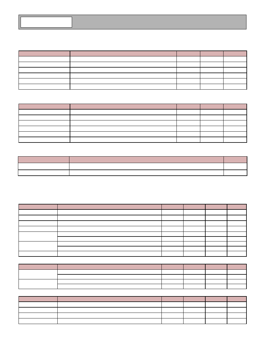
System Specifications
Absolute Maximum Ratings
Recommended Operating Conditions
ESD Rating
Electrical Characteristics
DC Specification
(T
OP
=+25∞C, V
DD_IO
=3.0V)
AC Characteristics (T
OP
=+25∞C, V
DD_IO
=3.0V, C
LOAD
=15pF)
Current Consumption
(T
OP
=+25∞C, V
BATT_ANA
, V
BATT_DIG
= 3.3 V)
Parameter
Description
Min
Max
Unit
V
CC
Analog circuit supply voltage
-0.3
3.63
V
V
DD_IO
I/O supply voltage
-0.3
3.63
V
V
BATT_ANA
Analog regulator supply voltage
-0.3
3.63
V
V
BATT_DIG
Digital regulator supply voltage
-0.3
3.63
V
T
ST
Storage temperature
-55
+125
∞C
RF
MAX
Maximum RF input level
≠
+5
dBm
Absolute maximum ratings indicate limits beyond which the useful life of the device may be impaired or damage may occur.
Parameter
Description
Min
Max
Unit
T
OP
Operating temperature (industrial grade)
-40
+85
∞C
T
EOP
Extended operating temperature
-40
+105
∞C
V
BATT_ANA
Supply for internal analog voltage regulator
2.3
3.63
V
V
BATT_DIG
Supply for internal digital voltage regulator
2.3
3.63
V
V
CC
Analog supply voltage
1.71
1.89
V
V
DD_IO
Digital interface I/O supply voltage
1.62
3.63
V
Symbol
Description
Rating
ESD
ESD protection - all pins
1
, human body model
2000 V
ESD
ESD protection - all pins, machine model
200 V
1
This device is a high performance RF integrated circuit with an ESD rating of 2,000 volts (HBM conditions per Mil-Std-883, Method
3015). Handling and assembly of this device should only be done using appropriate ESD controlled processes.
Symbol
Description
Min.
Typ.
Max.
Unit
V
IL
Input low voltage
GND-0.1
≠
0.3*V
DD_IO
V
V
IH
Input high voltage
0.7*V
DD_IO
≠
V
DD_IO
V
V
OL
Output low voltage
GND
≠
0.2*V
DD_IO
V
V
OH
Output high voltage
0.8*V
DD_IO
≠
V
DD_IO
V
I
OH
Output high current
≠
500
≠
µA
Output high current (pins 16, 19)
≠
4
≠
mA
I
OL
Output low current
≠
500
≠
µA
Output low current (pins 16, 19)
≠
4
≠
mA
I
ILI
Input leakage current
≠
<1
1
µA
Symbol
Description
Min.
Typ.
Max.
Unit
t
r
Rise time
≠
≠
30
ns
Rise time (pins 16, 19)
≠
≠
16
ns
t
f
Fall time
≠
≠
24
ns
Fall time (pins 16, 19)
≠
≠
13
ns
Symbol
Description
Min.
Typ.
Max.
Unit
I
DD_SLEEP
Current during sleep mode
≠
8
30
µA
I
DD_IDLE
Current during idle, synthesizer not running
≠
3
5
mA
I
DD_TRANSMIT
Current during continuous transmit
≠
55
65
mA
I
DD_RECEIVE
Current during continuous receive
≠
68
75
mA
5 of 12
SiW1711
60 0047 R00Grf SiW1711 Radio Modem IC DS
Digital Regulator Specification
(T
OP
= 25∞C)
Internal Analog Voltage Regulator Specification
(T
OP
=+25∞C, V
BATT_ANA
= 3.3 V
)
Radio Specification
RF Impedances
Receiver Specification
1
(V
BATT_ANA
, V
BATT_DIG
=3.3V, V
CC
=int. analog reg. output, and nominal
2
Bluetooth test conditions)
Parameter
Description
Min
Typ
Max
Unit
Output voltage
(I
OUT
= 10 mA)
1.55
1.85
2.16
V
Line regulation
(I
OUT
= 0 mA, V
BATT_DIG
= 2.3 V to 3.63 V)
≠
8.0
≠
mV
Load regulation
(I
OUT
= 3 mA to 80 mA)
≠
9.0
≠
mV
Dropout voltage
(I
OUT
= 10 mA)
≠
≠
250
mV
Output maximum current
≠
≠
≠
80
mA
Quiescent current
≠
≠
10
≠
µA
Ripple rejection
f
RIPPLE
= 400 Hz
≠
40
≠
dB
Parameter
Description
Min
Typ
Max
Unit
Output voltage (40 mA load)
≠
1.71
1.80
1.89
V
Ripple rejection
≠
≠
20
≠
dB
Parameter
Description
Min
Typ
Max
Unit
VCO operating range
Frequency
2402
≠
2480
MHz
PLL lock time
≠
≠
55
100
µs
Parameter
1
Description
Min
Typ
Max
Unit
RF impedance
TX On
≠
448//0.6
≠
/pF
TX Off
≠
53.1//2.2
≠
/pF
RX On
≠
267//1.1
≠
/pF
RX Off
≠
23.4//0
≠
/pF
1
The impedance values are for typical samples in 32-pin QFN package.
Parameter
Description
Min
Typ
Max
Unit
Receiver
sensitivity
BER<0.1%
≠
-85.0
-80.0
dBm
Maximum usable signal
BER<0.1%
-10
0
≠
dBm
C/I co-channel
(0.1% BER)
Co-channel selectivity
≠
8.0
11.0
dB
C/I 1MHz
(0.1% BER)
Adjacent channel selectivity
≠
-4.0
0
dB
C/I 2MHz
(0.1% BER)
2nd adjacent channel selectivity
≠
-38.0
-35.0
dB
C/I
3MHz
(0.1% BER)
3rd adjacent channel selectivity
≠
-43
-40
dB
Out-of-band
blocking
3
30MHz to 2000MHz
-10
≠
≠
dBm
2000MHz to 2399MHz
-27
≠
≠
dBm
2498MHz to 3000MHz
-27
≠
≠
dBm
3000MHz to 12.75GHz
-10
≠
≠
dBm
Intermodulation
Max interferer level to maintain 0.1% BER,
interference signals at 3 MHz and 6 MHz offset.
-39
-36
≠
dBm
Receiver spurious
emission
30MHz to 1GHz
≠
≠
-57
dBm
1 GHz to 12.75 GHz
≠
≠
-47
dBm
1
Measured with a proper matching circuit without bandpass filter.
2
Nominal and extreme Bluetooth test conditions as defined by the Bluetooth Test and Interoperability Working Group published RF Test
Specification 1.1.
3
Out-of-band blocking guaranteed by design.

6 of 12
SiW1711
60 0047 R00Grf SiW1711 Radio Modem IC DS
Transmitter Specification
1
(V
BATT_ANA
, V
BATT_DIG
= 3.3 V, V
CC
= int. analog reg. output, and nominal Bluetooth test conditions)
Industrial Temperature Performance
1
(V
BATT_ANA
, V
BATT_DIG
=3.3V and extreme Bluetooth test conditions)
Parameter
Description
Min
Typ
Max
Units
Output RF
transmit power
At maximum power output level
-2.0
+2.0
+6.0
dBm
Modulation
Characteristics
2
f1
avg
140.0
-155.0
-175.0
kHz
f2
max
(For at least 99.9% of all f2
max
)
-115.0
≠
≠
kHz
f1
avg
/f2
avg
-0.8
≠
≠
kHz
Initial carrier
frequency
accuracy
≠
-75.0
≠
+75.0
kHz
Carrier frequency drift
One slot packet
-25.0
≠
+25.0
kHz
Two slot packet
-40.0
≠
+40.0
kHz
Five slot packet
-40.0
≠
+40.0
kHz
Max drift rate
≠
≠
400
Hz/
µs
20 dB occupied bandwidth
Bluetooth specification
≠
900
1000
kHz
In-band spurious emission
2MHz offset
≠
-74.0
-55.0
dBm
>3MHz offset
≠
-74.0
-55.0
dBm
Out-of-band
spurious
emission
30MHz to 1GHz, operating mode
≠
-70.0
-55.0
dBm
1GHz to 12.75GHz, operating mode
3
≠
-70.0
-50.0
dBm
1.8GHz to 1.9GHz
≠
≠
-62.0
dBm
5.15GHz to 5.3GHz
≠
≠
-47.0
dBm
1
Measured with a proper matching circuit without bandpass filter.
2
The modulation characteristic is measured as per test TRM/CA/07/C defined in the Bluetooth Test Specification.
3
Except transmit harmonics.
Parameter
Description
Min
Typ
Max
Units
Receiver
sensitivity
BER<0.1%
≠
-85.0
-75.0
dBm
Output RF transmit power
At maximum power output level
-4.0
+2.0
+6.0
dBm
Modulation
Characteristics
2
f1
avg
140.0
155.0
175.0
kHz
f2
max
(For at least 99.9% of all f2
max
)
115.0
≠
≠
kHz
f1
avg
/f2
avg
0.8
≠
≠
kHz
Initial carrier frequency
accuracy
≠
-75.0
≠
+75.0
kHz
Carrier frequency drift
One slot packet
-25.0
≠
+25.0
kHz
Two slot packet
-40.0
≠
+40.0
kHz
Five slot packet
-40.0
≠
+40.0
kHz
Max drift rate
≠
≠
+400
Hz/µs
20 dB occupied bandwidth
Bluetooth specification
≠
900
1000
kHz
In-band spurious emission
2MHz offset
≠
-74.0
-40.0
dBm
>3MHz offset
≠
-74.0
-55.0
dBm
Out-of-band
spurious
emission
30MHz to 1GHz, operating mode
≠
-70.0
-55.0
dBm
1GHz to 12.75GHz, operating mode
3
≠
-70.0
-40.0
dBm
1.8GHz to 1.9GHz
≠
≠
-62.0
dBm
5.15GHz to 5.3GHz
≠
≠
-47.0
dBm
1
Measured with a proper matching circuit without bandpass filter.
2
The modulation characteristic is measured as per test TRM/CA/07/C defined in the Bluetooth Test Specification.
3
Except transmit harmonics.

7 of 12
SiW1711
60 0047 R00Grf SiW1711 Radio Modem IC DS
External Reference Requirements
It is possible to provide a number of reference frequencies that are typical on most cellular phones directly into pin 25
(XTAL_P/CLK) of the device. The following reference frequencies (in MHz) can be used: 3.84, 9.6, 12, 12.8, 13, 14.4,
15.36, 16, 16.8, 19.2, 19.68, 19.8, 26, 32, 38.4, and 48 MHz. For other frequencies, please contact applications support.
Crystal Requirements
If using a crystal as the source for the reference frequency, the typical parameters are outlined below. The system clock
crystal should operate in a fundamental, parallel resonant mode.
Parameter
Description
Min
Max
Unit
Phase noise
100 kHz offset
≠
-100
dBc/Hz
1 kHz offset
≠
-120
dBc/Hz
10 kHz offset
≠
-140
dBc/Hz
Drive level
AC coupled amplitude
0.5
V
CC
V
P-P
DC coupled low peak voltage
0
0.3
V
DC coupled high peak voltage
V
CC
- 0.3
V
CC
V
Parameter
Description
Min
Typ
Max
Units
Drive level
≠
0.5
≠
2.0
V
P-P
ESR
Effective serial resistance
1
≠
≠
150
CO
Holder capacitance
2
≠
3.0
5.0
pF
CL
Load capacitance
2
≠
12.0
18.0
pF
CM
Motional capacitance
≠
6.0
≠
fF
1
For 32MHz crystal.
2
The actual values for CO and CL are dependent on the crystal manufacturer and can be compensated for by an internal crystal calibra-
tion capability.

8 of 12
SiW1711
60 0047 R00Grf SiW1711 Radio Modem IC DS
Radio Modem Application Circuit
SP
I
_
SELECT
C1
2
18
pF
R5 47
K
B
B
_C
LK
C2
2
22
pF
C3
8.
2pF
RX_
T
X_D
A
T
A
RESET
_
N
SP
I
_
MI
S
O
U1
S
i
W
171
1
1
2
3
4
5
6
7
8
9
10
11
12
13
14
15
16
17
18
19
20
21
22
23
24
25
26
27
28
29
30
31
32
ID
A
C
VREF
P_C
A
P
VREF
N_
CAP
VCC
_
O
U
T
VB
AT
T
_
ANA
VCC
CH
G
_
P
U
M
P
ENABL
E_
RM
TX_R
X_
SW
IT
C
H
RES
ET
_N
SPI_
RX
D
SPI_
CL
K
SPI_
TX
D
VDD_
IO
BB_
CLK
VB
B_O
U
T
V
B
A
TT_
D
I
G
RX
_
T
X
_
D
A
T
A
VBB
_
RD
Y
CD
_T
XE
N
SP
I
_
S
S
H
O
P_ST
R
O
BE
XTA
L
_
N
XTA
L_P/
CL
K
VCC
VTU
NE
VCC
RF_O
UT
VCC
RF_I
N
VCC
SP
I
_
MO
SI
CD
_T
X_EN
HO
P_
S
T
R
O
B
E
Y1 O
S
C
,
CR
Y
S
T
A
L
3
2
M
Hz
1
3
ENABLE_R
M
SP
I
_
C
L
K
L1
15
nH
V
B
B
_
RDY
C2
0
1u
F
C1
1
.0
1
u
F
C1
3
18
pF
C2
3
18
0pF
No
te
:
T
h
is
typi
ca
l
application ci
r
c
uit
is
suitab
l
e
for the
f
o
ll
owing conditions:
1
)
R
F
matching
circuit based
on
a typical
F
R
-
4
P
C
B
mater
i
a
l
and stand
ard QF
N package.
2
)
P
o
wer sup
p
ly
from
externa
l
sour
c
e
i
n
to inter
nal
v
o
l
t
age re
gulator
s
.
3
)
C
1
6
and
C20 must
have 1
oh
m <
ES
R <
10 o
h
ms.
4
)
L
5
value ma
y
va
ry
de
pending
upon layou
t
.
5
)
S
ee
A
p
p
l
ications fo
r
PC
B layout
requ
i
r
emen
ts.
VCC
L4 3.
3nH
C1 8.
2 pF
L3 3.
3
n
H
C2 2.
2p
F
L5 3.
3nH
C5 1.
5pF
L2 3.
9
n
H
C9
2.
7pF
C1
6
1uF
C8
2.
7p
F
C1
5
0.
1u
F
C1
4
0.
1u
F
L5 18n
H
C1
9
1p
F
VD
D_
A
VDD
_
D
VD
D_
I
O
I
N
OU
T
FL
1
M
u
ra
t
a
F
ilt
e
r
4
2
AN
TE
NNA

9 of 12
SiW1711
60 0047 R00Grf SiW1711 Radio Modem IC DS
Pin Out
(Top View)
Pin Assignments
Pin
Pin Name
Pin
Pin Name
1
IDAC
17
VBB_OUT
2
VREFP_CAP
18
VBATT_DIG
3
VREFN_CAP
19
RX_TX_DATA
4
VCC_OUT
20
VBB_READY
5
VBATT_ANA
21
CD_TXEN
6
VCC
22
SPI_SS
7
VCC
23
HOP_STROBE
8
CHG_PUMP
24
XTAL_N
9
ENABLE_RM
25
XTAL_P/CLK
10
TX_RX_SWITCH
26
VCC
11
RESET_N
27
VTUNE
12
SPI_RXD
28
VCC
13
SPI_CLK
29
RF_OUT
14
SPI_TXD
30
VCC
15
VDD_IO
31
RF_IN
16
BB_CLK
32
VCC
VC
C
RF_IN
VC
C
RF_OUT
XTAL_P/CLK
VC
C
VTUNE
VC
C
VBATT_ANA
IDAC
VCC
VCC
VREFN_CAP
VREFP_CAP
VCC_OUT
CHG_PUMP
E
N
ABLE_RM
TX_RX_SW
IT
CH
RE
SET_N
BB_CLK
VDD_IO
SPI
_TXD
SPI
_CLK
S
P
I_RXD
XTAL_N
HOP_STROBE
SPI_SS
VBB_OUT
VBATT_DIG
RX_TX_DATA
VBB_READY
CD_TXEN
1
2
3
4
5
6
7
8
9
10
11
12
13
14
15
16
17
18
19
20
21
22
23
24
25
26
27
28
29
30
31
32
GROUND PAD
ON BOTTOM

10 of 12
SiW1711
60 0047 R00Grf SiW1711 Radio Modem IC DS
Packaging and Product Marking
Package Drawing
32-Pin, QFN Drawing and Dimensions
Symbol
Min
Nom
Max
Notes:
A
0.8
≠
1.0
1. Coplanarity applies to leads, corner leads, and die attach pads.
A1
0
≠
0.05
2. All dimensions in mm.
A2
0.75
≠
1.0
b
0.18
0.25
0.3
D
5 BSC
E
5 BSC
e
0.5 BSC
J
3.52
3.62
3.72
K
3.52
3.62
3.72
L
0.35
0.4
0.45
C
A
B
0.1 M
32X b
32X L
16
9
25
32
1
8
17
24
K
B
A
C
0.1
e
e/2
N
J
B
A
C
0.1
VIEW M-M
EXPOSED DIE
ATTACH PAD
A1
A2
A
SEATING PLANE C
C
0.08
C
0.1
DETAIL G
VIEW ROTATED 90∞ CLOCKWISE
PIN 1 I.D.
DETAIL N
G
M
M
PIN 1 CORNER
A
D
B
C
0.1

11 of 12
SiW1711
60 0047 R00Grf SiW1711 Radio Modem IC DS
Product Marking
32-Pin, QFN Drawing
Part Number
Operational Temperature Range
1
Package
Ordering Quantity
SiW1711FIF
Industrial
32-pin QFN
490 per tray
SiW1711FIF-T13
Industrial
32-pin QFN
5,000 on 13" reel
SiW1711DIF-B
Industrial
KGD with bumps
100 per waffle pack
SiW1711DIF-T13
Industrial
KGD with bumps
5,000 on 13" reel
1
Industrial temperature range: -40∞C to +85∞C
XXXXXX
LLLLL
Pin 1 Corner
SIW
Pin 1 Bar
Trace Code
Lot Number

12 of 12
SiW1711
60 0047 R00Grf SiW1711 Radio Modem IC DS
RF Micro Devices believes the furnished information is correct and accurate at the time of this printing. RF Micro
Devices reserves the right to make changes to its products without notice and advises customers to verify that
the information being used is current. The described products are not designed, manufactured or intended for
use in equipment for medical, life support, aircraft control or navigation, or any other applications that require
failsafe operation. RF Micro Devices does not assume responsibility for the use of the described products.
RF MICRO DEVICESÆ, RFMDÆ, Providing Communication SolutionsTM, the diamond logo design, Silicon Wave,
and the SiW product name prefix are trademarks of RFMD, LLC. BLUETOOTHÆ is a trademark owned by
Bluetooth SIG, Inc., U.S.A. and licensed for use by RF Micro Devices, Inc. Manufactured under license from ARM
Limited. ARM, ARM7TDMI and the ARM logo are the registered trademarks of ARM Limited in the EU and other
countries. All other product, service, and company names are trademarks, registered trademarks or service
marks of their respective owners.