Document Outline
- Radio Features
- Baseband Features
- Standard Protocol Stack Features
- Additional Protocol Stack Features
- External System Interfaces
- Host HCI Transport (UART)
- Host HCI Transport (3-Wire UART)
- Audio Codec Interface
- Multi-function I/Os (MFPs)
- External Memory Interface
- Auxiliary UART
- External Power Amplifier Interface
- Power Management
- General-Purpose Analog to Digital Converter (ADC)
- External EEPROM Controller and Interface
- General System Requirements
- System Reference Clock
- Low Power Clock
- Power Supply Description
- RF I/O Description
- On-Chip Memory
- Configuration Selection
- Reference Frequency Selection
- Application Software Memory Selection
- The SiW3500 can support application (protocol stack) software execution from internal ROM or external FLASH memory. To run from internal ROM, pins D[9] and D[10] must be connected together as shown in the application circuit section of this d...
- Pin Description
- Table 1. SiW3500 Radio Processor Pin List
- System Specifications
- Absolute Maximum Ratings
- Recommended Operating Conditions
- ESD Rating
- Electrical Characteristics
- DC Specification (TOP = +25�C, VDD_P = 3.0 V)
- AC Characteristics (TOP = +25�C, VDD_P = 3.0 V, CLOAD = 15 pF)
- Current Consumption (TOP = +25�C, VBATT = 3.0 V using internal regulators)
- Digital Regulator Specification (TOP = 25�C)
- Radio Specification
- Receiver Specification1 (VBATT = 3.3 V, VCC = internal analog regulator output, TOP = 25�C)
- Transmitter Specification1 (VBATT = 3.3 V, VCC = internal analog regulator output, TOP = 25�C)
- Industrial Temperature Performance1 (VBATT= 2.3 - 3.63 V, VCC = internal analog regulator output, TOP = -40 to +85�C)
- Analog Voltage Supply Requirements
- External Reference Requirements
- Reference Crystal Requirements
- Application Circuit
- Internal ROM Version
- Application Circuit
- External Flash Version
- Ordering Information
14-37
RF Micro Devices, Inc.
7628 Thorndike Road
Greensboro, NC 27409, USA
Tel (336) 664 1233
Fax (336) 664 0454
http://www.rfmd.com
Product Description
Features
Optimum Technology MatchingÆ Applied
Si BJT
Si Bi-CMOS
GaInP/HBT
GaAs HBT
SiGe HBT
GaN HEMT
GaAs MESFET
Si CMOS
SiGe Bi-CMOS
Ordering Information
LNA
90
0
ADC
PLL
Synthesizer
DRIVER
90
0
Power
Control
RF_I/O
GFSK
Modem
DAC
ADC
DAC
Bluetooth
Link
Controller
ARM7TDMIÆ
Processor
Data SRAM
Firmware ROM
UART
Multi Function
I/Os
Audio CODEC
Interface
VT
UN
E
CH
G
_
P
U
M
P
VBAT
T
_
AN
A
VBAT
T
_
D
I
G
VC
C_
O
U
T
VBB_
O
U
T
VD
D_
P
AD
DR
ESS
BUS
DA
T
A
BU
S
C
S
, OE
a
n
d
W
E
PLL
Control
Voltage Regulators and
Power Distribution
Optional flash interface
C
L
K
_
RE
Q_
OU
T
CL
K_
R
E
Q
_
I
N
XT
AL
_
P
/
C
L
K
XT
AL
_
N
Clock Distribution
Internal
50-Ohm
Match
Network
Aux ADC
Block Diagram
SiW3500
ULTIMATEBLUE
The UltimateBlue SiW3500TM is a RF System On Chip (SoC) that combines
a 2.4 GHz transceiver, baseband processor, and protocol stack software for
BluetoothÆ wireless technology. Due to its low power CMOS process, the
SiW3500 is ideally suited for applications such as mobile phones, audio
headsets, and other embedded products.
The SiW3500 integrates an ARM7TDMI processor for software execution
from either internal ROM or external FLASH memory. The standard
SiW3500 ROM contains the Bluetooth lower layer stack software including
the HCI transport driver.
The SiW3500 is packaged in a 6 x 6 Pb-Free 96-VFBGA that meets RoHS
(Green) requirements. Known Good Die (KGD) is available for special
applications.
∑ RF System on Chip (SoC) for
Bluetooth wireless technology
combining a
2.4 GHz transceiver,
baseband processor, and protocol
stack ROM.
∑ Bluetooth specification V1.2 qualified
including mandatory and optional
functions such as AFH and eSCO.
∑ Manufactured using standard
0.18-micron CMOS process
technology.
∑ UART based Host Control Interface
(HCI) transport layer supports
standard and 3-wire modes.
∑ Direct conversion RF architecture
improves receiver
-blocking
performance.
∑ I/O voltage supply can range from
1.62 V to 3.63 V.
∑ -85 dBm receiver sensitivity and
+2 dBm transmitter power typical
performance specifications
.
∑ Integrated analog and digital voltage
regulators simplify system design.
∑ 50
RF I/O does not need any
additional external impedance
matching components.
∑ Flexible reference clock source
options including crystal or direct
input from the host platform.
∑ Internal temperature compensated
transmitter and receiver circuits
deliver consistent performance from
-40∞ to +85
∞C.
∑ On-chip ROM software storage with
patch capability.
Applications
∑ Mobile phones and smart phones.
∑ Bluetooth audio headset.
∑ Bluetooth hands-free kit.
SiW3500
UltimateBlue
0
60 0066 R00Hrf SiW3500 Radio Processor DS
Preliminary
November 8, 2004

Preliminary
14-38
SiW3500
60 0066 R00Hrf SiW3500 Radio Processor DS
Radio Features
∑ RF System on Chip (SoC) for Bluetooth wireless technology combining a 2.4 GHz transceiver, baseband processor,
and protocol stack ROM.
∑ Bluetooth specification V1.2 qualified including mandatory and optional functions such as AFH and eSCO.
∑ Manufactured using standard 0.18 m CMOS process technology.
∑ UART based Host Control Interface (HCI) transport layer supports standard and 3-wire modes.
∑ Direct conversion RF architecture improves receiver-blocking performance.
∑ I/O voltage supply can range from 1.62 V to 3.63 V.
∑ -85 dBm receiver sensitivity and +2 dBm transmitter power typical performance specifications.
∑ Integrated analog and digital voltage regulators simplify system design.
∑ 50
RF I/O does not need any additional external impedance matching components.
∑ Flexible reference clock source options including crystal or direct input from the host platform.
∑ Internal temperature compensated transmitter and receiver circuits deliver consistent performance from -40∞ to
+85∞C.
∑ On-chip ROM software storage with patch capability.
Baseband Features
∑ Hardware based GFSK MODEM and packet processing contributes to lower system current consumption with
minimal software overhead.
∑ ARM7TDMI processor efficiently executes all protocol stack and application software.
∑ Software execution from either internal ROM or external FLASH memory. The SiW3500 features a ROM patch
mechanism that allows substituting small portions of ROM code with code either downloaded from the host or stored
in external EEPROM.
∑ Extensive multi function I/Os allow flexible product configurations.
∑ Auxiliary analog-to-digital converter (ADC) is available for applications such as battery level detection.
Standard Protocol Stack Features
∑ Full-featured lower layer Bluetooth protocol stack software up to the host interface (HCI).
∑ Bluetooth 1.2 qualified including mandatory and optional features such as AFH, extended SCO, faster connections,
and LMP improvements.
∑ Full Bluetooth connection capabilities with support for piconet and scatternet modes and device scanning during SCO
connection.
∑ Able to establish up to 3 SCO connections simultaneously.
∑ Supports low power connection states such as hold, sniff, and park modes with selectable sniff intervals.
∑ Full support of Bluetooth test modes for use during production.
∑ Verified HCI command level compatibility with multiple upper layer stack software.
Additional Protocol Stack Features
∑ Proprietary channel assessment algorithm provides fast and accurate determination of occupied channel for use in
AFH mode.
∑ In addition to AFH, UltimateBlue Coexistence Technology is part of the baseline protocol stack. UltimateBlue
coexistence minimizes interference to 802.11b/g products.
∑ The Channel Quality Driven Data Rate (CQDDR) feature optimizes data transfer in noisy or weak signal
environments.
∑ Full selection of upper layer protocol stack software and profiles available for license and customization.
Preliminary
14-39
SiW3500
60 0066 R00Hrf SiW3500 Radio Processor DS
[
= Included in SiW3500 ROM
External System Interfaces
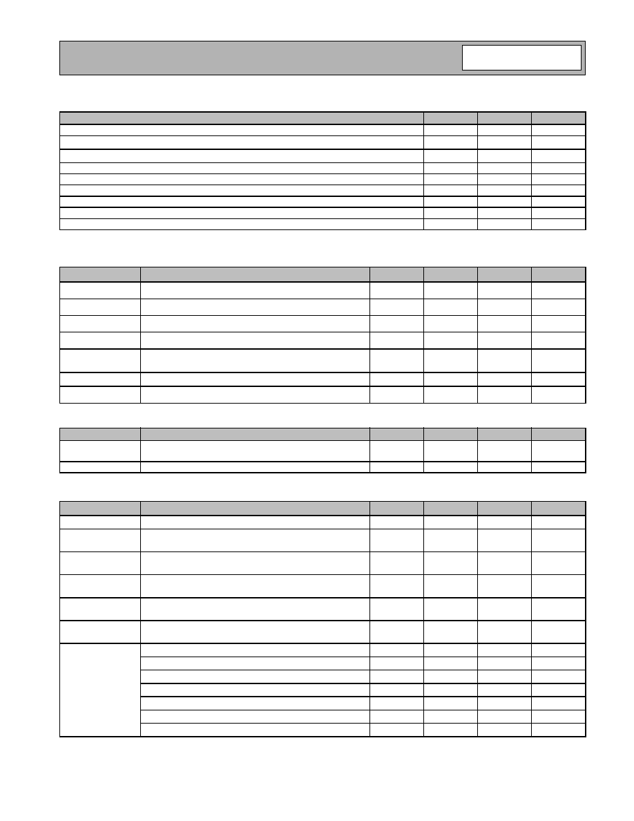
Host HCI Transport (UART)
The high speed UART interface provides the physical transport between the SiW3500 and the application host for the
transfer of Bluetooth data compliant
with the Bluetooth specification. The table below shows the supported configura-
tions. The default baud rate is 115,200 bps and can be set depending on the product.
Host HCI Transport (3-Wire UART)
To reduce the number of signals and to increase the reliability of the HCI UART interface, a 3-wire UART protocol is
available in the SiW3500. The protocol is compliant with the Bluetooth specification H:5 transport and backwards
compatible with the BCSP 3-wire UART protocol. Selection between H:4 UART, H:5 UART, and BCSP UART is done
automatically by the SiW3500.
Audio Codec Interface
The SiW3500 supports direct interface to an external audio CODEC or PCM host device. The interface provides the
following configurations:
∑ Standard PCM clock rates from 64 kHz to 2.048 MHz with multi-slot handshakes and synchronization.
∑ Supports either master or slave mode.
∑ Supports any PCM data size up to 16 bits.
∑ Compatible with Motorola SSI mode.
ROM Features
SiW3500
HCI
SiW3500
Headset
Protocol Stack
Lower stack up to HCI
[
[
UltimateBlue Coexistence
[
[
Upper Stack (L2CAP, SDP, RFCOMM)
≠
[
Programming Interface (API)
≠
[
Profiles
Headset Profile (HSP)
≠
[
Hands Free Profile (HFP)
≠
[
SiW3500 Radio Processor HCI UART Parameters
Required Host Setting
Number of data bits
8
Parity bit
No parity
Stop bit
1 stop bit
Flow control
RTS/CTS
Host flow-off response requirement from the SiW3500
8 bytes
SiW3500 IC flow-off response requirement from host
2 bytes
Supported baud rates
9.6k, 19.2k, 38.4k, 57.6k, 115.2k, 230.4k, 460.8k, 500k, 921.6k,
1M, 1.5M, 2M
SiW3500 Radio Processor HCI 3-Wire UART Parameters
Required Host Setting
Number of data bits
8
Parity bit
Even
Stop bit
1 stop bit
Error detection
SLIP and checksum
Sleep modes
Shallow and deep
Preliminary
14-40
SiW3500
60 0066 R00Hrf SiW3500 Radio Processor DS
∑ Configuration of the CODEC interface is done by the firmware during boot-up by reading non-volatile memory (NVM)
parameters.
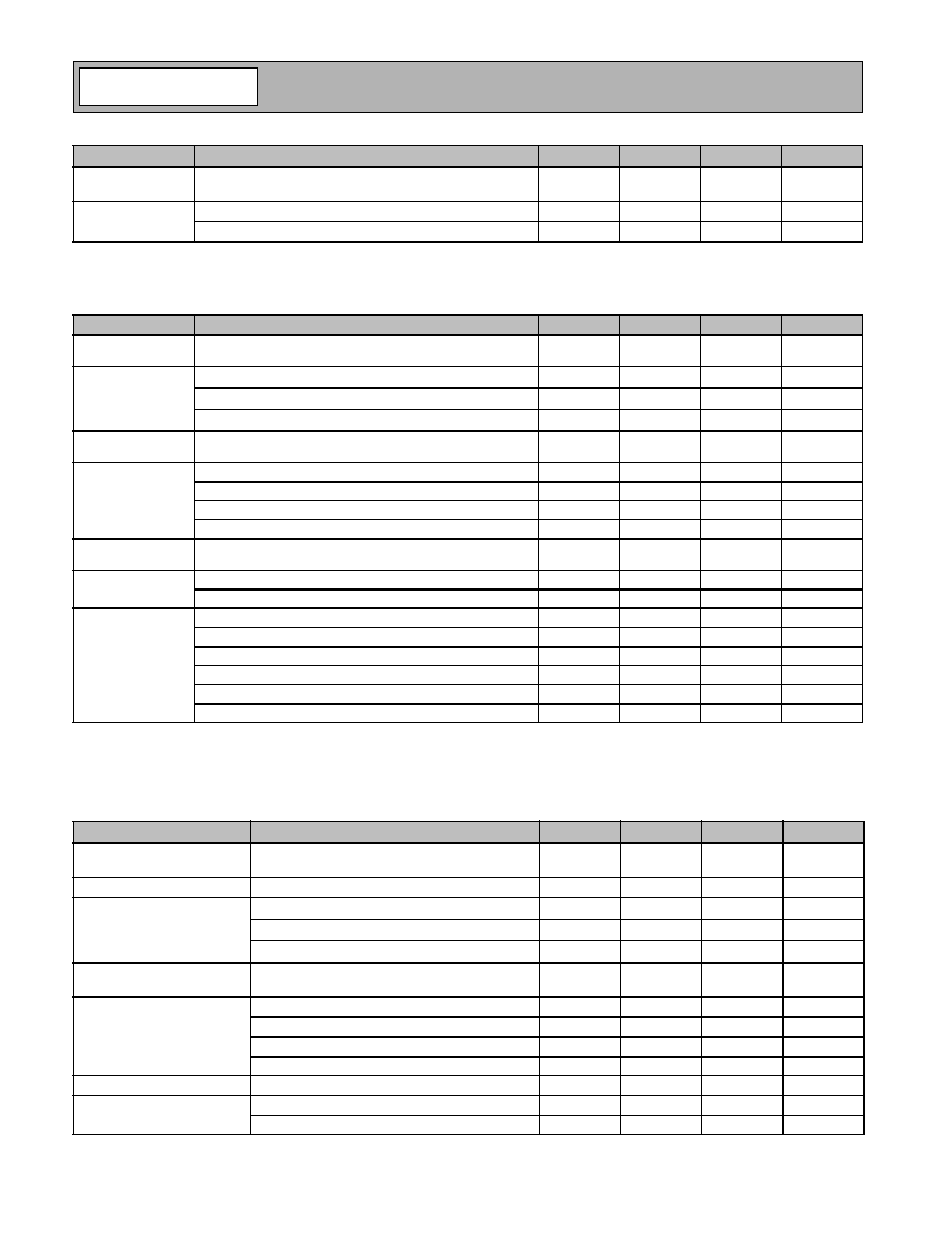
Multi-function I/Os (MFPs)
Up to 8 (eight) multi-function I/O ports are available in the SiW3500. The table below identifies the I/Os and their usage.
External Memory Interface
The SiW3500 does not require additional memory for standard below HCI protocol functions. An external memory
interface is available for execution of protocol stack software from FLASH memory if desired. If external FLASH memory
will be used, the read access time of the device must be 100 ns or less.
Auxiliary UART
The SiW3500 can be configured and enabled with an auxiliary UART port. This UART port can be used for debug
depending on the application software.
External Power Amplifier Interface
The SiW3500 supports the use of an external power amplifier for +20 dBm designs. When enabled, these signals
provide an integrated interface for the control of an external PA.
Power Management
The HOST_WAKEUP and EXT_WAKE signals are used for power management control of the SiW3500.
HOST_WAKEUP is an output signal used to indicate Bluetooth activity to the host. EXT_WAKE is an input signal used
by the host to wake up the SiW3500 from sleep mode.
For control of the reference clock source, CLOCK_REQ_IN and CLOCK_REQ_OUT can be made available to turn on/off
an external reference clock source.
General-Purpose Analog to Digital Converter (ADC)
The SiW3500 incorporates a general-purpose ADC
that can be enabled to sample external analog voltage. The ADC
has an 8-bit resolution.
External EEPROM Controller and Interface
This interface is intended for communication to an optional EEPROM when using the SiW3500 in ROM mode. The
Multi Function I/O Number
Possible Usage Configuration
MFP[0]
General purpose.
MFP[1]
CLOCK_REQ_IN, HOST_WAKEUP, General purpose.
MFP[2]
Address A[18], SYNC_CLOCK, AUX_RTS, General purpose.
MFP[3]
FREQ_SEL[3], SYNC_DATA, General purpose.
MFP[4]
FREQ_SEL[1], General purpose.
MFP[5]
FREQ_SEL[2], General purpose.
MFP[6]
AUX_RXD, General purpose.
MFP[7]
AUX_CTS, TX_RX_SWITCH, General purpose.
Signal
Description
AUX_TXD
TX Data
AUX_RXD
RX Data
AUX_CTS
Clear To Send
AUX_RTS
Request To Send
Signal
Description
IDAC
Power control to external PA. This output provides a variable current source
that can be used to control the external PA. Leave unconnected if not used
TX_RX_SWITCH
Output signal used to indicate the state of the radio. This could be used as a
direction control for the PA. The polarity is programmable with the default set
as: Low = Transmit; High = Receive.
Preliminary
14-41
SiW3500
60 0066 R00Hrf SiW3500 Radio Processor DS
EEPROM is not required for configurations with external flash. The EEPROM is the non-volatile memory (NVM) in the
system and contains the system configuration parameters such as the Bluetooth device address, the CODEC type, as
well as other parameters. These default parameters are set at the factory, and some parameters will change depending
on the system configuration. Optionally, the memory parameters can be downloaded from the host processor at boot up
eliminating the need for EEPROM. Please consult the Application Support team for details. The EEPROMs should have
a serial I
2
C interface with a minimum size of 2 Kbits and 16-byte page write buffer capabilities.
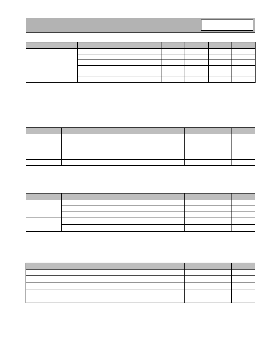
General System Requirements
System Reference Clock
The SiW3500 chip can use either an external crystal or a reference clock as the system clock input. A partial list of
supported frequencies (in MHz) includes: 9.6, 12, 12.8, 13, 14.4, 15.36, 16, 16.8, 19.2, 19.68, 19.8, 26, 32, 38.4, and 48.
For other frequencies, please contact Applications Support. The system reference crystal/clock must have an accuracy
of ±20 PPM or better to meet the Bluetooth specification.
Low Power Clock
For the Bluetooth low power clock, a 32.768 kHz crystal can be used to drive the SiW3500 oscillator circuit, or alterna-
tively, a 32.768 kHz reference clock signal can be used instead of a crystal. If the lowest power consumption is not
required during low-power modes such as sniff, hold, park, and idle modes, the 32.768 kHz crystal may be omitted in the
design.
If the 32.768 kHz clock source is used, the clock source should be connected to the CLK32_IN pin and must meet the
following requirements:
∑ For AC-coupled via 100 pF or greater (peak-to-peak voltage):
400 mV
P-P
< CLK32_IN < V
DD_C
∑ For DC-coupled:
CLK32_IN minimum peak voltage < V
IL
CLK32_IN maximum peak voltage > V
IH
Where V
IL
= 0.3 * V
DD_C
Where V
IH
= 0.7 * V
DD_C
∑ For both cases, the signal is not to exceed:
-0.3 V < CLK32_IN < V
DD_C
+ 0.3 V
Power Supply Description
The SiW3500 operates at 1.8 V core voltage for internal analog and digital circuits. The chip has internal analog and
digital voltage regulators simplifying power supply requirements to the chip. The internal voltage regulators can be
supplied directly from a battery or from other system voltage sources. Optionally, the internal regulators can be by-
passed if 1.8 V regulated source is available on the system.
Note: Both regulators can be bypassed if external regulation is desired. When bypassing the analog regulator, the VBATT_ANA and VCC_OUT pins
must be tied together and the external analog voltage (1.8 V) should be applied to the VBATT_ANA pin. When bypassing the digital regulator, the
VBATT_DIG pin should be left unconnected and the external digital voltage (1.8 V) should be applied to VBB_OUT pin.
The power for the I/Os is taken from two separate sources (V
DD_P
and
V
DD_P_ALT
). They can range from 1.62 to 3.63
Function
Internal Analog Regulator
Internal Digital Regulator
Regulator input pin
V
BATT_ANA
= 2.3 to 3.63 V
V
BATT_DIG
= 2.3 to 3.63 V
Regulator output pin
V
CC_OUT
= 1.8 V
V
DD_C
= 1.8 V
I
nternal Regulator Used
Function
Analog Core Circuits
Digital Core Circuits
Circuit voltage supply pin
V
CC
= 1.8 V
V
DD_C
= 1.8 V
Internal Regulator Bypassed
Preliminary
14-42
SiW3500
60 0066 R00Hrf SiW3500 Radio Processor DS
Volts to maintain compatibility with a wide range of peripheral devices. Please check the pin list for the exact pins that are
powered from the V
DD_P
and V
DD_P_ALT
sources.
RF I/O Description
The SiW3500 employs single-ended RF input and output pins for reduced external components. In typical Class 2 (0
dBm nominal) applications, no external matching components are necessary.
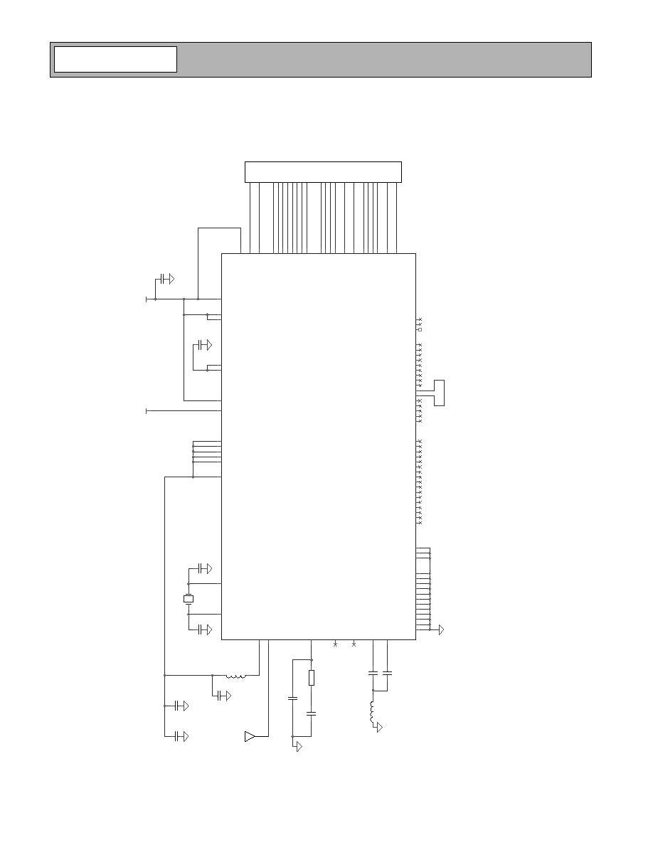
On-Chip Memory
The SiW3500 Radio Processor integrates both SRAM and ROM. The ROM is pre-programmed with Bluetooth protocol
stack software (HCI software) and boot code that executes automatically upon reset. The boot code serves to control the
boot sequence as well as to direct the execution to the appropriate memory for continued operation.
Configuration Selection
Reference Frequency Selection
The SiW3500 is designed to operate with multiple reference frequencies. During boot, specific frequency select I/O pins
are sampled to determine the default reference frequency. The reference frequency setting will be set according to the
following table:
Application Software Memory Selection
The SiW3500 can support application (protocol stack) software execution from internal ROM or external FLASH
memory. To run from internal ROM, pins D[9] and D[10] must be connected together as shown in the application circuit
section of this document (Application Circuit). To run from external flash memory, the flash must be connected as shown
in the application circuit diagram and contain valid application code. If the external memory does not have valid program
data, the device enters a download mode in which a valid program may be loaded into the external memory through a
sequence of commands over the HCI transport layer.
FREQ_SEL3
(MFP[3])
FREQ_SEL2
(MFP[5])
FREQ_SEL1
(MFP[4])
FREQ_SEL0
(ADC_IN)
Frequency
0
0
0
0
15.36 MHz
0
0
0
1
19.2 MHz
0
0
1
0
19.44 MHz
0
0
1
1
19.68 MHz
0
1
0
0
19.8 MHz
0
1
0
1
26 MHz
0
1
1
0
38.4 MHz
0
1
1
1
Do not program frequency (leave as ref/2 and set
according to system parameters).
1
0
X
X
32 MHz
1
1
0
0
32 MHz
1
1
0
1
12 MHz
1
1
1
0
13 MHz
1
1
1
1
14.4 MHz
Preliminary
14-43
SiW3500
60 0066 R00Hrf SiW3500 Radio Processor DS
Pin Description
The following table provides detailed listings of pin descriptions arranged by functional groupings.
Name
Pad Type
Ball
Description
Radio (Power from VCC)
RF_IO
Analog
A2
RF signal. Input and output.
TX_BIAS
Analog
A4
Internal transmitter driver bias.
VTUNE
Analog
A6
Pin for reference PLL loop filter, only used if reference frequency is not
integer multiples of 4 MHz.
CHG_PUMP
Analog
F1
Pin for RF loop filter.
XTAL_N
Analog
B7
System clock crystal negative input. If a reference clock is used, this pin
should be left unconnected.
XTAL_P/CLK
Analog
A7
System clock crystal positive input or reference clock input.
IDAC
Analog
B1
Power control to external power amplifier. This output provides a variable
current source that can be used to control the external power amp. Leave
unconnected if not used.
ADC_IN
Analog
J2
Analog to digital converter input or FREQ_SEL_(0)
.
VREFN_CAP
Analog
C2
Decoupling capacitor for internal A/D converter voltage reference.
VREFP_CAP
Analog
C1
Decoupling capacitor for internal A/D converter voltage reference.
Low Power Oscillator and Reset (Power from VDD_P_ALT)
CLK32K_IN
Analog
L1
For crystal or external clock input (32.768 kHz).
CLK32K_OUT
Analog
K1
Drive for crystal.
RESET_N
CMOS input
G1
System level reset (active low).
Power Control Interface (Power from VDD_P)
PWR_REG_EN
CMOS bi-directional
G2
CLOCK_REQ_OUT control line for external TCXO by default, or can be
used as enable for an external voltage regulator. Programmable active
high or active low.
AUX_TXD
CMOS bi-directional
G9
Auxiliary UART serial port output.
Multi-function (MFP) I/O (Power from VDD_P)
MFP [0]
CMOS bi-directional
F3
Multi-function I/O port.
MFP [1]
CMOS bi-directional
J1
Multi-function I/O port.
MFP [2]
CMOS bi-directional
L6
Multi-function I/O port.
MFP [3]
CMOS bi-directional
F10
Multi-function I/O port.
MFP [4]
CMOS bi-directional
B9
Multi-function I/O port.
MFP [5]
CMOS bi-directional
C8
Multi-function I/O port.
MFP [6]
CMOS bi-directional
C7
Multi-function I/O port.
MFP [7]
CMOS bi-directional
C6
Multi-function I/O port.
PCM Interface (Power from VDD_P_ALT)
PCM_IN
CMOS bi-directional
H3
PCM data output from SiW3500.
PCM_OUT
CMOS bi-directional
L2
PCM data input to SiW3500.
PCM_CLK
CMOS bi-directional
K3
PCM synchronous data clock to the remote device. Normally an output.
Input for slave mode.
PCM_SYNC
CMOS bi-directional
K2
PCM synchronization data strobe to the remote device. Normally an out-
put. Input for slave mode.
Table 1. SiW3500 Radio Processor Pin List
Preliminary
14-44
SiW3500
60 0066 R00Hrf SiW3500 Radio Processor DS
UART Interface (Power from VDD_P_ALT)
UART_RXD
CMOS input
G3
UART receive data.
UART_TXD
CMOS output
L4
UART transmit data.
UART_CTS
CMOS input
H2
UART flow control clear to send.
UART_RTS
CMOS output
H1
UART flow control ready to send.
EXT_WAKE
CMOS input
C5
Wake up signal from host.
External Memory Interface (power from VDD_P)
A[17]
A[16]
A[15]
A[14]
A[13]
A[12]
A[11]
A[10]
A[9]
A[8]
A[7]
A[6]
A[5]
A[4]
A[3]
A[2]
A[1]
CMOS output
E11
J11
L5
F11
B8
K6
L7
A10
H11
A11
B11
K9
K7
C10
K10
D10
L11
Address lines.
Note: A[17] and A[16] can be used to support an optional external serial
EEPROM when using the internal ROM in place of the external Flash
memory.
D[15]
D[14]
D[13]
D[12]
D[11]
D[10]
D[9]
D[8]
D[7]
D[6]
D[5]
D[4]
D[3]
D[2]
D[1]
D[0]
CMOS bi-directional
A9
C9
B10
E10
K5
G11
G10
H9
K4
J9
K8
J6
J5
F9
J4
H10
Data lines.
Note: Connect D[9] to D[10] to use internal ROM.
OE_N
CMOS output
L10
Output enable for external memory (active low).
WE_N/EEPROM_WP
CMOS output
A8
Write enable for external memory (active low).
FCS_N
CMOS output
J10
Chip select for external memory (active low).
Power and Ground
VBATT_ANA
Power
D3
Positive supply to internal analog voltage regulator.
VBATT_DIG
Power
L9
Positive supply to internal digital voltage regulator.
VCC_OUT
Power
D1
Regulated output from internal analog voltage regulator.
VDD_P
Power
D11
K11
Positive supply for external memory interface and some digital I/Os.
VDD_C
Power
C11
L8
Positive supply for digital circuitry or output of internal digital voltage.
Name
Pad Type
Ball
Description
Table 1. SiW3500 Radio Processor Pin List (Continued)

Preliminary
14-45
SiW3500
60 0066 R00Hrf SiW3500 Radio Processor DS
VCC
Power
A1
B6
C4
E1
E3
Positive supply for RF and analog circuitry.
VSS_P
GND
J8
E9
Ground connections for VDD_P.
VDD_P_ALT
Power
L3
Positive supply for UART, CODEC, and other digital I/Os.
VSS_P_ALT
Ground
J3
Ground connection for VDD_P_ALT.
GND
GND
A3
A5
B2
B3
B4
B5
C3
D2
E2
F2
D9
J7
Ground connections for RF and analog circuitry.
Name
Pad Type
Ball
Description
Table 1. SiW3500 Radio Processor Pin List (Continued)
Preliminary
14-46
SiW3500
60 0066 R00Hrf SiW3500 Radio Processor DS
System Specifications
Absolute Maximum Ratings
Recommended Operating Conditions
ESD Rating
Electrical Characteristics
DC Specification
(T
OP
=+25∞C, V
DD_P
=3.0V)
AC Characteristics
(T
OP
=+25∞C, V
DD_P
=3.0V, C
LOAD
=15pF)
Parameter
Description
Min
Max
Unit
V
DD_C
Digital circuit supply voltage
-0.3
3.63
V
V
CC
Analog circuit supply voltage
-0.3
3.63
V
V
DD_P,
V
DD_P_ALT
I/O supply voltage
-0.3
3.63
V
V
BATT_ANA
Analog regulator supply voltage
-0.3
3.63
V
V
BATT_DIG
Digital regulator supply voltage
-0.3
3.63
V
T
ST
Storage temperature
-55
+125
∞C
RF
MAX
Maximum RF input level
≠
+5
dBm
Note: Absolute maximum ratings indicate limits beyond which the useful life of the device may be impaired or damage may occur.
Parameter
Description
Min
Max
Unit
T
OP
Operating temperature (industrial grade)
-40
+85
∞C
T
EOP
Extended operating temperature
1
-40
+105
∞C
V
BATT_ANA
Unregulated supply voltage into internal analog regulator
2.3
3.63
V
V
BATT_DIG
Unregulated supply voltage into internal digital regulator
2.3
3.63
V
V
CC
Regulated supply voltage directly into analog circuits
1.71
1.89
V
V
DD_C
Regulated supply voltage directly into digital circuits
1.62
1.98
V
V
DD_P ,
V
DD_P_ALT
Digital interface I/O supply voltage
1.62
3.63
V
1.The extended operating temperature range applies to special order devices qualified for extended operating range. Please contact factory for details.
Symbol
Description
Rating
ESD
ESD protection - all pins
2000 V
Note: This device is a high performance RF integrated circuit with an ESD rating of 2,000 volts (HBM conditions per Mil-Std-883, Method 3015).
Handling and assembly of this device should only be done using appropriate ESD controlled processes.
Symbol
Description
Min.
Typ
Max.
Unit
V
IL
Input low voltage
GND-0.1
≠
0.3
.
V
DD_P
V
V
IH
Input high voltage
0.7
.
V
DD_P
≠
V
DD_P
V
V
OL
Output low voltage
GND
≠
0.2
.
V
DD_P
V
V
OH
Output high voltage
0.8
.
V
DD_P
≠
V
DD_P
V
I
OH
Output high current
≠
1
≠
mA
I
OL
Output low current
≠
1
≠
mA
I
ILI
Input leakage current
≠
1
≠
µA
Symbol
Description
Typ
Max.
Unit
t
r
Rise time
5
11
ns
t
f
Fall time
5
8
ns
Preliminary
14-47
SiW3500
60 0066 R00Hrf SiW3500 Radio Processor DS
Current Consumption
(T
OP
=+25∞C, V
BATT
=3.0V using internal regulators)
*
Note: Continuous transmit and receive currents are measured in operating modes where there is no activity in baseband digital circuits.
Digital Regulator Specification
(T
OP
= 25∞C)
Radio Specification
Receiver Specification
1
(V
BATT
=3.3V, V
CC
=internal analog regulator output, T
OP
= 25∞C)
Operating Mode
Average
Max
Unit
Standby
40
80
µA
Continuous transmit
*
48
55
mA
Continuous receive
*
54
60
mA
Parked slave, 1.28 sec. interval
90
≠
µA
Inquiry scan, 1.28 sec interval
440
≠
µA
Page scan, 1.28 sec. interval
560
≠
µA
ACL connection, sniff mode, 40 ms interval
1.3
≠
mA
ACL data transfer 723 kbps TX, 57 kbps RX
42
≠
mA
SCO connection, HV3 packets
22
≠
mA
Parameter
Description
Min
Typ
Max
Unit
Output voltage
(I
OUT
= 10 mA)
1.62
1.80
1.98
V
Line regulation
(I
OUT
= 0 mA, V
BATT_DIG
= 2.3 V to 3.63 V)
≠
8.0
≠
mV
Load regulation
(I
OUT
= 3 mA to 80 mA)
≠
9.0
≠
mV
Dropout voltage
(I
OUT
= 10 mA)
≠
≠
250
mV
Output maximum
current
Maximum supplied current while maintaining regulation
≠
≠
80
mA
Quiescent current
Off current
≠
10
≠
µA
Ripple rejection
f
RIPPLE
= 400 Hz
≠
40
≠
dB
Parameter
Description
Min
Typ
Max
Unit
VCO Operating
Range
Frequency
2402
≠
2480
MHz
PLL lock time
Average tune time
≠
60
100
µs
Parameter
Description
Min
Typ
Max
Unit
Receiver sensitivity
BER < 0.1%
≠
-85
-78
dBm
Maximum
usable signal
BER < 0.1%
-10
0
≠
dBm
C/I co-channel
(0.1% BER)
Co-channel selectivity
≠
+8.0
+10.0
dB
C/I 1 MHz
(0.1% BER)
Adjacent channel selectivity
≠
-4.0
-3.0
dB
C/I 2 MHz
(0.1% BER)
2nd adjacent channel selectivity
≠
-38.0
-35.0
dB
C/I
3 MHz
(0.1% BER)
3rd adjacent channel selectivity
≠
-43.0
-40.0
dB
Out-of-band
blocking
2
Fc/3
-23
≠
≠
dBm
Fc/2
-25
≠
≠
dBm
2 * Fc/3
-45
≠
≠
dBm
30 MHz - 2000 MHz
-10
≠
≠
dBm
2000 MHz - 2399 MHz
-27
≠
≠
dBm
2498 MHz - 3000 MHz
-27
≠
≠
dBm
3000 MHz - 12.75 GHz
-10
≠
≠
dBm
Preliminary
14-48
SiW3500
60 0066 R00Hrf SiW3500 Radio Processor DS
1. Measured into the chip with 50
source and no bandpass filter.
2. Out-of-band blocking guaranteed by design.
Transmitter Specification
1
(V
BATT
=3.3V, V
CC
=internal analog regulator output, T
OP
= 25∞C)
1. Measured into the chip with 50
source and no bandpass filter.
2. Modulation characteristics as measured per test TRM/CA/07/C as defined in the Bluetooth test specification.
Industrial Temperature Performance
1
(V
BATT
=2.3
≠
3.63V, V
CC
=internal analog regulator output,
T
OP
= -40 to +85∞C)
Intermodulation
Max interferer level to maintain 0.1% BER, interference sig-
nals at 3 and 6 MHz offset.
-39
-36
≠
dBm
Receiver spurious
emission
30 MHz to 1 GHz
≠
≠
-57
dBm
1 GHz to 12.75 GHz
≠
≠
-47
dBm
Parameter
Description
Min
Typ
Max
Unit
Output RF transmit
power
At maximum power output level
-2
+2
+5
dBm
Modulation
Characteristics
2
f1
avg
140
155
175
kHz
f2
max
(For at least 99.9% of all f2
max
)
115
≠
≠
kHz
f1
avg
/ f2
avg
0.8
≠
≠
kHz
Initial carrier
frequency accuracy ≠
-75
≠
+75
kHz
Carrier frequency
drift
One slot packet
-25
≠
+25
kHz
Two slot packet
-40
≠
+40
kHz
Five slot packet
-40
≠
+40
kHz
Max drift rate
≠
≠
20
kHz/50 µs
20 dB occupied
bandwidth
Test per Bluetooth specification
≠
≠
1000
kHz
In-band spurious
emission
2 MHz offset
≠
≠
-40
dBm
>3 MHz offset
≠
≠
-60
dBm
Out-of-band
spurious
emission
30 MHz to 1 GHz, operating mode
≠
≠
-55
dBm
30 MHz to 1 GHz, idle mode
≠
≠
-57
dBm
1 GHz to 12.75 GHz, operating mode
≠
≠
-50
dBm
1 GHz to 12.75 GHz, idle mode
≠
≠
-47
dBm
1.8 GHz to 1.9 GHz
≠
≠
-62
dBm
5.15 GHz to 5.3 GHz
≠
≠
-47
dBm
Parameter
Description
Min
Typ
Max
Unit
Receiver
sensitivity
BER<0.1%
≠
-85
-75
dBm
Output RF transmit power
At maximum power output level
-4
+2
+6
dBm
Modulation
Characteristics
2
f1
avg
140
155
175
kHz
f2
max
(For at least 99.9% of all f2
max
)
115
≠
≠
kHz
f1
avg
/ f2
avg
0.8
≠
≠
kHz
Initial carrier frequency
accuracy
≠
-75
≠
+75
kHz
Carrier frequency drift
One slot packet
-25
≠
+25
kHz
Two slot packet
-40
≠
+40
kHz
Five slot packet
-40
≠
+40
kHz
Max drift rate
≠
≠
20
kHz/50 µs
20 dB occupied bandwidth
Bluetooth specification
≠
≠
1000
kHz
In-band spurious emission
2 MHz offset
≠
≠
-40
dBm
>3 MHz offset
≠
≠
-60
dBm
Parameter
Description
Min
Typ
Max
Unit
Preliminary
14-49
SiW3500
60 0066 R00Hrf SiW3500 Radio Processor DS
Analog Voltage Supply Requirements
The SiW3500 processor is designed for use with its own internal low noise analog voltage regulator. This configuration is
recommended for all applications. When necessary, the internal analog regulator can be bypassed. In situations where
bypassing the internal analog regulator is required, the supply voltage to the analog circuit must satisfy the following
requirements to preserve the RF performance characteristics.
External Reference Requirements
It is possible to provide a number of reference frequencies that are typical in most cellular phones directly into ball B7
(XTAL_P/CLK) of the device. Refer to "System Reference Clock" on page 41 for a list of supported reference
frequencies.
Reference Crystal Requirements
Many reference frequencies are supported by the device. If a crystal is used as the reference frequency source, the
typical required parameters are listed below:
1. For 32 MHz crystal.
2. If DC-coupled, the external reference signal voltage must stay within this range at all times.
3. The actual values for C
O
and C
L
are dependent on the crystal manufacturer and can be compensated for by an internal crystal calibration
capability.
Out-of-band
spurious
emission
30 MHz to 1GHz, operating mode
≠
≠
-55
dBm
30 MHz to 1GHz, idle mode
≠
≠
-57
dBm
1 GHz to 12.75 GHz, operating mode
≠
-70
-50
dBm
1 GHz to 12.75 GHz, idle mode
≠
≠
-47
dBm
1.8 GHz to 1.9 GHz
≠
≠
-62
dBm
5.15 GHz to 5.3 GHz
≠
≠
-47
dBm
1.
Measured into the chip with 50
impedance and no bandpass filter. Industrial temperature performance guaranteed by design.
2.
The modulation characteristic is measured as per test TRM/CA/07/C defined in the Bluetooth Test Specification.
Parameter
Description
Min
Max
Unit
VCC
Analog supply voltage to all VCC input pins
1.71
1.89
V
Minimum
load current
External regulator current
80
≠
mA
Minimum
ripple rejection
At 400Hz
40
≠
dB
Output noise
Integrated 10 Hz to 80 kHz noise
≠
22
mV RMS
Parameter
Description
Min
Max
Unit
Phase noise
100 Hz offset
≠
-100
dBc/Hz
1 kHz offset
≠
-120
dBc/Hz
10 kHz offset
≠
-140
dBc/Hz
Drive level
AC amplitude
0.5
V
CC
V
P-P
DC level
a
a.If DC-coupled, the external reference signal voltage must stay within this range at all times.
0.3
V
CC
V
Parameter
Description
Min
Typ
Max
Unit
Drive level
≠
≠
≠
0.3
mW
ESR
Effective serial resistance
1
≠
≠
150
C
O
Holder capacitance
2
≠
3
5
pF
C
L
Load capacitance
3
≠
12
18
pF
C
M
Motional capacitance
≠
6
≠
fF
Parameter
Description
Min
Typ
Max
Unit
Preliminary
14-50
SiW3500
60 0066 R00Hrf SiW3500 Radio Processor DS
Application Circuit
Internal ROM Version
HOST I
NTERFACE
C4
1
8pF
U1
C4
B1
C2
C1
D1
D3
E3
F1
G2
E11
J11
F11
L7
H9
H10
J4
J6
F9
L4
K8
J5
A10
A11
K6
F3
C11
H2
C5
K9
H11
G3
L9
J3
L3
J2
K1
L1
A8
G10
L6
K4
G11
K2
K3
K5
D11
L2
K7
C10
H3
H1
D10
K10
J9
B10
L11
C9
A9
B11
E10
B8
L10
K11
J10
L8
J1
L5
G1
B7
A7
B6
A6
E1
A4
A1
A2
J8
E9
A3
A5
B2
B3
B4
B5
C3
D9
D2
E2
F2
J7
F10 B9 C8 C7 C6
G9
VCC
ID
A
C
V
R
EF
P_C
A
P
V
R
E
F
N_
CA
P
VCC_OUT
VBATT_
ANA
VCC
CHG_
P
U
M
P
PW
R
_
R
E
G
_
E
N
A[17
]/EEP
RO
M_SCL
A[16
]/EEP
RO
M_SDA
A[14
]
A[11
]
D[8]/P
IO[3
]
D[0]
D[1]
D[4]/P
IO[4
]
D[2]
UART_TX
D
D[5]/P
IO[5
]
D[3]
A[10
]
A[8]
A[12
]
MFP
[
0
]
VDD_C
UART_C
T
S
EX
T_WAK
E
A[6]
A[9]
UA
R
T
_R
X
D
VBATT
_DIG
VSS
_P_A
LT
VDD_P_
ALT
AD
C
_
IN
CL
K
3
2
K
_O
U
T
CL
K
32K_I
N
WE_N/E
EPROM_W
P
D[9]
MFP
[
2
]
D[7]/P
IO[7
]
D[10]
P
C
M
_
SYN
C
PCM_CLK
D[11]
VDD_
P
PC
M_
O
U
T
A[5]
A[4]
PCM_I
N
UART_R
T
S
A[2]
A[3]
D[6]/P
IO[6
]
D[13]
A[1]
D[14]
D[15]
A[7]
D[12]
A[13
]
OE_N
VDD_
P
FCS_N
VDD_C
MP
F[
1
]
A[15
]
R
E
SET
_
N
XTAL_N
XTAL
_P/
CLK
VCC
VT
U
N
E
VCC
TX
_
B
I
A
S
VCC
RF
_I
O
VSS_P
VSS_P
GND
GND
GND
GND
GND
GND
GND
GND
GND
GND
GND
GND
MFP
[
3
]
MFP
[
4
]
MFP
[
5
]
MFP
[
6
]
MFP
[
7
]
AU
X_
T
X
D
SiW3
500
VBA
T
T
C5 18pF
C3 1
.
5pF
C1
0
0
.
1
u
F
Co
nn
ec
t D[
9]
to
D[
10
] to
s
e
l
ect
in
te
rn
al
R
O
M
mo
de
.
VDD
_
P
An
te
nn
a
R1 47K
C1
1
0
.
1
u
F
C6 1u
F
C
9
180pF
Y1
D
S
X321SL
1
3
C8
2
2pF
C7
8.2pF
C2 1u
F
C1 0.1uF
(IN
TERNAL
ROM C
ONFIG
URATIO
N)
L1 2.
2n
H
L2 18nH
Preliminary
14-51
SiW3500
60 0066 R00Hrf SiW3500 Radio Processor DS
Application Circuit
External Flash Version
C1 0.
1
u
F
U2
2
M
or
4M
F
L
A
S
H
E1
D1
C1
A1
B1
D2
C2
A2
B5
A5
C5
D5
B6
A6
C6
D6
E6
B2
G1
A4
F1
A3
B3
C3
D3
B4
C4
D4
F6
E2
H2
E3
H3
H4
E4
H5
E5
F2
G2
F3
G3
F4
G5
F5
G6
G4
H1
H6
A0
A1
A2
A3
A4
A5
A6
A7
A8
A9
A10
A11
A12
A13
A14
A15
A16
A17
OE
WE
CE
R
Y
/
BY#
NC
NC
NC
RE
SE
T#
NC
NC
BY
TE
#
DQ0
DQ1
DQ2
DQ3
DQ4
DQ5
DQ6
DQ7
DQ8
DQ9
DQ10
DQ11
DQ12
DQ13
DQ14
DQ15
VCC
GND
GND
C1
1
0
.
1
u
F
(
EXTERN
AL FL
ASH CO
NFIGUR
ATION)
C
9
180pF
R1
47K
VBA
T
T
Y1
1
3
HOST INTERFACE
SiW3
500
C8
2
2pF
C7
8.2pF
C1
2
0.1uF
C6 1u
F
MF
P[
2]
VD
D
_
P
No
te
: Fo
r 4M
Fl
as
h,
u
s
e
M
PF[
2]
fo
r A1
7 pi
n
C2 1uF
An
te
nn
a
C1
0
0
.
1
u
F
VDD
_
P
C5 18pF
U1
C4
B1
C2
C1
D1
D3
E3
F1
G2
E11
J11
F11
L7
H9
H10
J4
J6
F9
L4
K8
J5
A10
A11
K6
F3
C11
H2
C5
K9
H11
G3
L9
J3
L3
J2
K1
L1
A8
G10
L6
K4
G11
K2
K3
K5
D11
L2
K7
C10
H3
H1
D10
K10
J9
B10
L11
C9
A9
B11
E10
B8
L10
K11
J10
L8
J1
L5
G1
B7
A7
B6
A6
E1
A4
A1
A2
J8
E9
A3
A5
B2
B3
B4
B5
C3
D9
D2
E2
F2
J7
F10 B9 C8 C7 C6
G9
VCC
ID
A
C
V
R
EF
P_C
A
P
V
R
E
F
N_
CA
P
VCC
_O
UT
VBA
TT_ANA
VCC
CHG_
P
U
M
P
PW
R
_
R
E
G
_
E
N
A[17
]/E
EP
RO
M_SC
L
A[16
]/E
EP
RO
M_SD
A
A[14]
A[11]
D[8
]/P
IO[3
]
D[0]
D[1]
D[4
]/P
IO[4
]
D[2]
UART_TX
D
D[5
]/P
IO[5
]
D[3]
A[10]
A[8]
A[12]
MFP
[
0
]
VDD_
C
UART_C
T
S
EX
T_WAK
E
A[6]
A[9]
UA
R
T
_R
X
D
VBAT
T_D
IG
VSS_
P_AL
T
VDD
_P_
ALT
AD
C
_
IN
CL
K
3
2
K
_O
U
T
CL
K
32K_I
N
WE
_N
/EEP
RO
M_W
P
D[9]
MFP
[
2
]
D[7
]/P
IO[7
]
D[10]
P
C
M
_
SYN
C
PCM_CLK
D[11]
VDD_
P
PC
M_
O
U
T
A[5]
A[4]
PCM_I
N
UART_R
T
S
A[2]
A[3]
D[6
]/P
IO[6
]
D[13]
A[1]
D[14]
D[15]
A[7]
D[12]
A[13]
OE_N
VDD_
P
FCS_N
VDD_
C
MP
F[
1
]
A[15]
R
E
SET
_
N
XTAL
_N
XT
AL_P/C
LK
VCC
VT
U
N
E
VCC
TX
_
B
I
A
S
VCC
RF
_I
O
VSS_
P
VSS_
P
GND
GND
GND
GND
GND
GND
GND
GND
GND
GND
GND
GND
MFP
[
3
]
MFP
[
4
]
MFP
[
5
]
MFP
[
6
]
MFP
[
7
]
AU
X_
T
X
D
C3 1.
5
p
F
C4
1
8pF
L1 2.
2n
H
L2 18
nH
DSX
321
S
L
Preliminary
14-52
SiW3500
60 0066 R00Hrf SiW3500 Radio Processor DS
VFBGA I/O Configuration (Top View)
1
2
3
4
5
6
7
8
9
10
11
A
B
C
D
E
F
G
H
J
K
L
VCC
RF_IO
GND
VREF
P_CAP
GND
GND
GND
VREF
N_CAP
VCC_
OUT
GND
VCC
GND
IDAC
GND
VCC
VTUNE
EXT_
WAKE
GND
TX_
BIAS
VCC
VBATT_
ANA
MFP[7]
GND
A[9]
D[4]
D[9]
D[7]
MFP[5]
D[3]
A[11]
D[11]
A[13]
XTAL_
P/CLK
MFP[3]
GND
VDD_P
D[2]
UART_
CTS
MFP[1]
CLK_
32K_
OUT
CHG_
PUMP
CLK_
32K_
IN
GND
A[1]
D[13]
A[3]
A[15]
FCS_N
VDD_C
A[8]
PCM_
CLK
VCC
PCM_
OUT
AUX_
XTD
MFP[6]
UART_
RTS
MFP[0]
RESET_
N
MFP[2]
A[17]
A[12]
A[16]
OE_N
GND
A[14]
MFP[4]
D[12]
D[10]
VDD_P
WE_N
XTAL_N
A[5]
A[4]
D[14]
A[7]
UART_
TXD
UART_
RXD
VDD_
P_ALT
PCM_IN
PWR_
REG_
EN
PCM_
SYNC
D[6]
ADC_IN
A[6]
VSS_P
D[15]
VDD_C
D[8]
D[1]
D[0]
D[5]
A[2]
VBATT_
DIG
A[10]
VSS_P_
ALT
1
2
3
4
5
6
7
8
9
10
11
VSS_P
Preliminary
14-53
SiW3500
60 0066 R00Hrf SiW3500 Radio Processor DS
Packaging and Product Marking
Package Drawing
Green package, 96-Pin, 6 mm x6 mm, VFBGA Drawing and Dimensions
Symbol
Min
Max
Notes:
A
0.8
1.0
1. Dimension b is measured at the maximum solder ball diameter, parallel to datum plane Z.
A1
0.2
0.3
A2
0.22 REF
2. Datum Z is defined by the spherical crowns of the solder balls.
A3
0.45 REF
b
0.25
0.35
3. Parallelism measurement shall exclude any effect of mark on top surface of package.
D
6 BSC
E
6 BSC
4. All dimensions are in millimeters.
e
0.5 BSC
D1
5 BSC
5. VFBGA green package solder ball material: 95.5% Sn, 4% Ag, 0.5% Cu.
E1
5 BSC
Preliminary
14-54 of 54
SiW3500
60 0066 R00Hrf SiW3500 Radio Processor DS
The information in this publication is believed to be accurate and reliable. However, no responsibility
is assumed by RF Micro Devices for its use, nor for any infringement of patents, or other rights of
third parties, resulting from its use. No license is granted by implication or otherwise under any
patent or patent rights of RF Micro Devices, Inc. RF Micro Devices reserves the right to change
component circuitry, recommended application circuitry and specifications at any time without prior
notice.
RF MICRO DEVICESÆ, RFMDÆ, Optimum Technology MatchingÆ, Enabling Wireless ConnectivityTM,
UltimateBlueTM, and the SiW product name prefix are trademarks of RFMD, LLC. BLUETOOTH is a trademark
owned by Bluetooth SIG, Inc., U.S.A. and licensed for use by RF Micro Devices, Inc. Manufactured under license
from ARM Limited. ARM, ARM7TDMI and the ARM logo are the registered trademarks of ARM Limited in the EU
and other countries. All other trade names, trademarks and registered trademarks are the property of their
respective owners.
Product Marking
96-Pin, VFBGA Drawing
Ordering Information
Part Number
Operational
Temperature Range
1
Package
Ordering
Quantity
SIW3500GIG1
Industrial
96-pin VFBGA,
green package
429 pcs. per tray
SIW3500GIG1-T13
Industrial
96-pin VFBGA,
green package
2500 on 13" reel
SiW3500DIF1
Industrial
Known good die
2
,
green package
Waffle pack
SiW3500DIF1-T13
Industrial
Known good die
2
,
green package
2,500 on 13" reel
1
Industrial temperature range: -40∞C to +85∞C.
2
For additional technical details about known good die, please refer to RF Micro Devices document 60
0071 SiW3500DIF Bumped Die Manufacturing Notes.
XXXXXXXX
LLLLL
YYWW ARM
Pin 1 Corner
SIW
Pin 1 Bar
4 Digit
Date Code
Trace Code