 | –≠–ª–µ–∫—Ç—Ä–æ–Ω–Ω—ã–π –∫–æ–º–ø–æ–Ω–µ–Ω—Ç: RB5C634A | –°–∫–∞—á–∞—Ç—å:  PDF PDF  ZIP ZIP |

RB5C634A Technical Specification
Ver. 1.1.6 (Outline)
2005/03/07
1
RB5C634A
Technical Specification
Outline
(JPEG2000 Coder)
¶ The information contained in this document is subject to change without prior notice.
¶ The data sheet may not be copied or otherwise reproduced, in whole or in part, without prior written
consent of RICOH.

RB5C634A Technical Specification
Ver. 1.1.6 (Outline)
2005/03/07
2
1.
Outline...................................................................................................................................................................3
2.
Features ................................................................................................................................................................3
3.
Block Diagram and System Configuration Example................................................................................................5
3.1.
Block Diagram................................................................................................................................................5
3.2.
System Configuration Example.......................................................................................................................5
4.
Pin Functions.........................................................................................................................................................7
4.1.
Pin List............................................................................................................................................................7
4.2.
Pin Assignment...............................................................................................................................................9
4.3.
Pin Assignment Table...................................................................................................................................10
4.4.
Processing Speed .........................................................................................................................................11
5.
Electrical Characteristics......................................................................................................................................12
5.1.
Absolute Maximum Rating.............................................................................................................................12
5.2.
Recommended Operating Conditions............................................................................................................12
5.3.
DC Characteristics........................................................................................................................................12

RB5C634A Technical Specification
Ver. 1.1.6 (Outline)
2005/03/07
3
1.
Outline
The RB5C634A is a one-chip coder equipped with image compression function of generating JPEG2000-compliant
codes and decompression function of decoding images from the JPEG2000-compliant codes. Because of its superior
capability of creating the whole codestream including a main header, the RB5C634A is able to provide powerful encoding
and decoding functionality that is attained simply by setting up parameters in the internal registers. Using this coder, an
image of up to 1024 x 1024 pixels can be processed within one tile, which presents you with the ideal solution for
reducing the degradation in image quality to a large extent, even at the high compression level.
In addition, so-called rate control is supported; thus promising the flexible capability of controlling compressed codes to
any size.
With all these capabilities, the RB5C634A enables accurate and thorough control over the images, on a frame-basis, to
be stored without fail in predetermined storage devices. The RB5C634A will be one of the best solutions to users seeking
out precise image control, both in number and quality.
2.
Features
[I/O image data]
Precision:
8 bits/color/pixel when using IR9-7; 8, 10, 12 bits/color/pixel when using R5-3.
Sampling format:
1) YCbCr 4:2:2 (H2V1)
2) YCbCr 4:0:0 (Grayscale)
Image size:
Processes images of any size up to 1024 x 1024 pixels, in one-tile.
[Wavelet filter]
Selectable between R5-3 filter and IR9-7 filter
[Codestream]
- Rate control function that enables generation of a specific amount of codes
- Code recompression function (Code input
Code compression
Code output)
The Ricoh-proprietary algorithms allows automatic truncation so that the optimum image quality can be
obtained and generation of codes of the specified amount.
[Header processing]
Automatically generates a main header, a tile part header, and a packet header during compression, and
interprets them during decompression, internally.
[Decompression of reduced images]
Using the same code, a reduced image can be decompressed to the size of 1/1, 1/4, 1/16, 1/64, 1/128, and
1/256 of the original image.
[Processing speed]
- With truncation:
maximum of about 31M pixels/sec
For an image of 720 x 480 pixels (4:2:2), 90 frames can be compressed or decompressed per second. (In
such case, compression rate should be set to about 1/30.)
- Without truncation: maximum of about 27M pixels/sec
(Lossless when using R5-3 filter.)

RB5C634A Technical Specification
Ver. 1.1.6 (Outline)
2005/03/07
4
[Interface]
1) Image data interface is selectable from the following two:
- VSYNC Image Interface based on VSYNC, HSYNC, and FIELD input
Use this mode when connecting with a general-purpose video coder or encoder
- Image Frame Interface that transfers image data on a frame basis using handshake method
2) Code data interface is selectable from the following two:
- 16-bit Code Interface in the clock-based handshake method
- Access via PCI bus (target access)
3) Local data interface
8-bit wide local bus is used to enable data read/write from/to the internal registers
However, if the PCI bus is selected as the code data interface, access is enabled through the PCI.
4) SDRAM interface
32-bit wide SDRAM interface. SDRAM is used as storage of image data and as a work field during
processing. Connect SDRAM of 64M bits or more.
[Miscellaneous]
- Clock for Image data interface:
VSYNC Image mode:
Max. 33 MHz
Image Frame mode: Max. 45 MHz
- Clock for internal operations and SDRAM interfaces: Max. 90 MHz, Min. 40 MHz
(The minimum value is specified according to the lock range of the incorporated PLL for SDRAM clock
phase focusing)
- Clock for the PCI/local bus and Code Interface:
Max. 33 MHz
- I/O voltage: 3.3 V, Internal power supply voltage:
1.8 V
- PLL incorporated for SDRAM clock frequency synthesis
- Package: 272-pin BGA (size= 27 mm x 27 mm, pitch= 1.27 mm)

RB5C634A Technical Specification
Ver. 1.1.6 (Outline)
2005/03/07
5
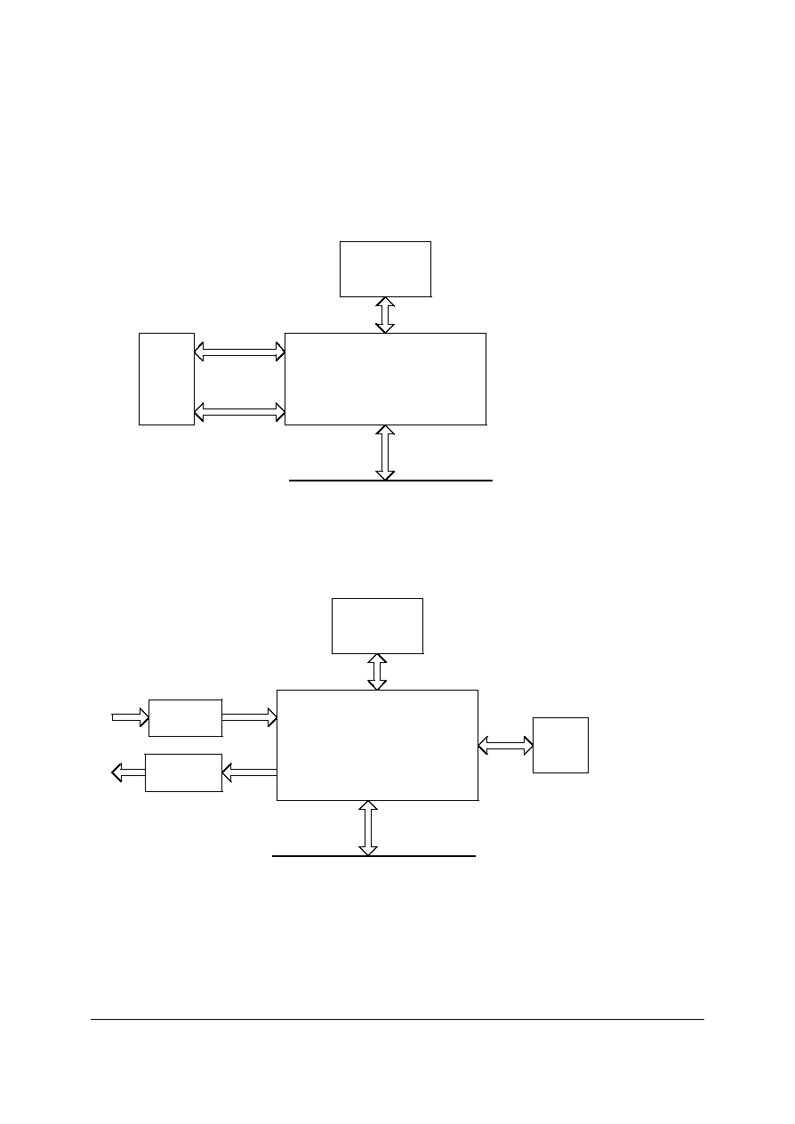
3.
Block Diagram and System Configuration Example
3.1. Block Diagram
SDRAM
Image
I/F
Wavelet
transform
R5:3
IR9:7
SDRAM
I/F
&
ARB
MQ
Coder
Packet
generater
Packet
decoder
CODE
I/F
REG
&
ctrl
Image
Data
I/F
Code
Data
I/F
HostI/F
(Without PCI)
3.2. System Configuration Example
1) Case 1
Image data: VSYNC Image Interface
Code data, Internal register access: PCI
RB5C634A
SDRAM
Video
Decoder
Video
Encoder
Image IN
Image
OUT
NTSC/
PAL
Code Data and
Command data I/F
PCI
RB5C634A Technical Specification
Ver. 1.1.6 (Outline)
2005/03/07
6
2) Case 2
Image data: Image Frame Interface
Code data: Code Interface
Internal register access: Local bus
3) Case 3
Image data: VSYNC Image mode
Code data: Code Interface
Internal register access: Local bus
RB5C634A
SDRAM
Image IN/OUT
Code IN/OUT
Internal Data Access
Image
and
Code
handle
LSI
Local BUS
RB5C634A
SDRAM
Video
Decoder
Video
Encoder
Image IN
Image OUT
NTSC/
PAL
Internal Data Access
Local BUS
Code
IN/OUT
Code
Handle
LSI

RB5C634A Technical Specification
Ver. 1.1.6 (Outline)
2005/03/07
7
4.
Pin Functions
4.1. Pin List
Block
Pin Name
Count I/O
Function
Up/
Down
Note *
OUTPUT
Drive
Note *
TTL
/CMOS
Note **
3-state
Clock
RESET_N
1
I System reset
CMOS
Reset
VCLK0
1
I
Video input/Pixel clock for
synchronous image bus
CMOS
VCLK1
1
I Pixel clock for video output
CMOS
PCLK
1
I
PCI/Local I/F, Clock input for
synchronous code bus
CMOS
MCLKI
1
I Clock input for internal operation and
SDRAM
CMOS
MCLKO
1
O Clock output for test purpose
8mA
CMOS
Analog
CPOUT
1
O PLL comparator output
Image
Data I/O
HSYNC0_N
(IMDFRM_N)
1
I/O
Video input HSYNC signal or SYNC
image bus ready input
U
8mA
CMOS
VSYNC0_N
(IMDRDYI_N)
1
I
Video input VSYNC signal or SYNC
image bus frame signal
U
CMOS
FIELD_ID0
(IMDRDYO_N)
1
I/O
Video input field recognition signal or
SYNC image bus ready output
U
8mA
CMOS
HSYNC1_N
1
I Video output HSYNC signal
U
CMOS
VSYNC1_N
1
I Video output VSYNC signal
U
CMOS
FIELD_ID1
1
I Video output field recognition signal
U
CMOS
VD
0-VDI7
8
I/O
Video input data bus 0-7,
Synchronous image I/O 0-7
U
8mA
CMOS
VDO0-VDO7
8
I/O Video output data bus 0-7,
Synchronous image I/O bus 8-15
U
8mA
CMOS
External CS0_N-CS3_N
4
O SDRAM chip select 0-3
12mA
CMOS
?
Memory WE_N
1
O SDRAM write strobe
12mA
CMOS
?
I/F1
DQM0-DQM3
4
O SDRAM data mask 0-3
12mA
CMOS
?
MA0-MA11
12
O SDRAM address bus 0-11
8mA
CMOS
?
BA0-BA1
2
O SDRAM bank address 0-1
8mA
CMOS
?
RAS_N
1
O SDRAM low address strobe
8mA
CMOS
?
CAS_N
1
O SDRAM column address strobe
8mA
CMOS
?
CKE0-CKE3
4
O SDRAM clock enable 0-3
12mA
CMOS
?
DQ0-DQ31
32
I/O SDRAM data bus 0-31
D
12mA
CMOS
PCI
PCI_FRAME_N
1
I/O PCI frame
PCI
PCI
PCI_IRDY_N
1
I/O PCI initiator ready
PCI
PCI
PCI_TRDY_N
(CODRDYI_N)
1
I/O PCI target ready
PCI
PCI
PCI_STOP_N
1
I/O PCI stop
PCI
PCI
PCI_IDSEL
1
I PCIID select
PCI
PCI_DEVSEL_N
(CODFRM_N)
1
I/O PCI device select
PCI
PCI
PCI_PERR_N
(CODRDYO_N)
1
I/O PCI parity error
PCI
PCI
PCI_AD0-PCI_AD31
32
I/O
PCI address, data bus 0-31
Local bus I/O signal
PCI
PCI
PCI_CB0-PCI_CB3
4
I/O PCI command bus 0-3
PCI
PCI
PCI_PAR
1
I/O PCI parity
PCI
PCI
Bus
switching
PCIF_SEL
1
I
Local bus ≠ PCI Switching
0: Local bus I/F
1: PCI
U
CMOS
Interrupt INT_N
1
O Interrupt output
4mA
N-ch
open drain
?
GIO0
1
I/O General purpose port 0
8mA
CMOS
General-
purpose
port
GIO1
1
I/O General purpose port 1
8mA
CMOS

RB5C634A Technical Specification
Ver. 1.1.6 (Outline)
2005/03/07
8
Block
Pin Name
Count I/O
Function
Up/
Down
Note *
OUTPUT
Drive
Note *
TTL
/CMOS
Note **
3-state
Test
TEST0-TEST2
3
I Test 0-2
CMOS
TESTOT
1
O Test output
12mA
CMOS
?
ATPGEN
1
I ATPG
CMOS
TRST
1
I JTAG reset
U
CMOS
TCK
1
I JTAG clock
CMOS
TMS
1
I JTAG mode select
U
CMOS
TDI
1
I JTAG data input
U
CMOS
TDO
1
O JTAG data output
4mA
CMOS
?
Total number of
signal lines
148
Power
VSSA1
1
G For PLL use
supply/
VDDA1
1
V For PLL use
GND
GND
55
G GND
VCC
41
V 1.8V
VCC2
26
V 3.3V
Total number of
power supplies,
GND
124
Total number of pins 272
Note *: PCI represents PCI compliance
Note **: ? represents JTAG only, whereas ? represents Normal operation.
Note (1): Some pin names have a suffix of `N,' which indicates that the corresponding signal is of negative logic. One
exception is TRST (JTAG reset), which is negative logic without this `N'. All the remaining signals without `N' are positive
logic.
Note (2): In normal operations, fix input of test pins as follows:
TEST0
=L
TEST1
=L
TEST2
=L
ATPGEN =L
TRST
=L
TCK
=L
TMS
=L
TDI
=H

RB5C634A Technical Specification
Ver. 1.1.6 (Outline)
2005/03/07
9
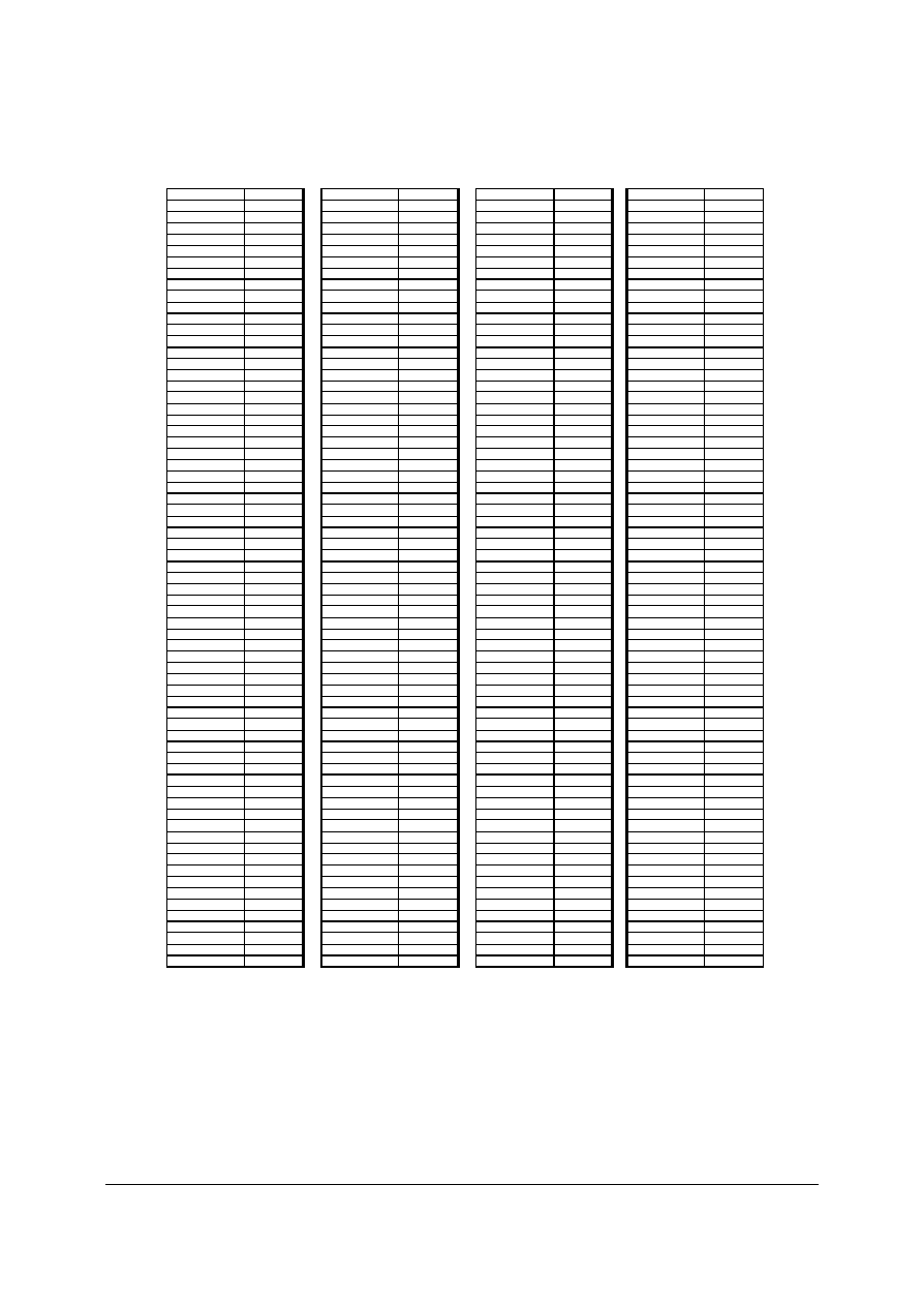
4.2. Pin Assignment
CKE2
CKE3
BA0
MA11
MA9
MA7
MA5
MA3
MA0
MCLKO
CPOUT
VSSA1
RESET_N
TCK
TMS
TEST0
VCLK1
VSYNC1_N
VDO07
VDO06
1
CS2_N
DQM3
BA1
MA10
MA8
MA6
MA4
MA2
MA1
TDO
VDDA1
TEST2
MCLKI
TRST
TDI
TEST1
FIELD_ID1 HSYNC1_N
VDO05
VDO04
2
CS3_N
DQM2
VCC2
VCC
VCC2
VCC
VCC
VCC2
VCC
VCC
GND
GND
GND
TESTOT
ATPGEN
VCC
VCC2
VCC
VDO03
VDO02
3
DQ30
DQ31
GND
GND
GND
GND
GND
GND
GND
VCC2
VCC
VCC2
VCC
VCC2
GND
GND
GND
GND
VDO01
VDO00
4
DQ28
DQ29
GND
VCC
VCC2
GIO0
VCLK0
FIELD_ID0
5
DQ26
DQ27
GND
VCC2
VCC
VCC
HSYNC0_N VSYNC0_N
6
DQ24
DQ25
GND
VCC
VCC2
GIO
VDI07
VDI06
7
DQ22
DQ23
GND
VCC
VCC
VCC
VDI05
VDI04
8
DQ20
DQ21
GND
VCC2
GND
GND
GND
GND
VCC2
PCIF_SEL
VDI03
VDI02
9
DQ18
DQ19
GND
VCC
GND
GND
GND
GND
VCC
VCC
VDI01
VDI00
10
CS1_N
DQ17
VCC
VCC2
GND
GND
GND
GND
VCC2
INT_N
PCI_AD31
PCLK
11
CS0_N
DQ16
VCC
VCC
GND
GND
GND
GND
VCC
GND
PCI_AD29
PCI_AD30
12
DQM0
DQM1
VCC2
VCC
VCC
GND
PCI_AD27
PCI_AD28
13
CKE1
CKE0
VCC
VCC2
VCC2
GND
PCI_AD25
PCI_AD26
14
DQ14
DQ15
GND
VCC
VCC
GND
PCI_CB3
PCI_AD24
15
DQ12
DQ13
GND
VCC2
VCC
GND
PCI_AD23 PCI_IDSEL
16
DQ10
DQ11
GND
VCC2
VCC2
GND
GND
GND
GND
GND
GND
GND
VCC
GND
GND
VCC
VCC
VCC2
PCI_AD21
PCI_AD22
17
DQ08
DQ09
VCC
VCC
VCC
VCC
VCC2
VCC
VCC2
VCC
VCC
VCC2
VCC
VCC2
VCC
VCC2
GND
GND
PCI_AD19
PCI_AD20
18
DQ07
DQ05
DQ03
DQ01
RAS_N
WE_N
PCI_AD1
PCI_AD3
PCI_AD5
PCI_AD7
PCI_AD8
PCI_AD10 PCI_AD12 PCI_AD14
PCI_CB1
PCI_PERR_
N
PCI_DEVSE
L_N
PCI_IRDY_
N
PCI_CB2
PCI_AD18
19
DQ06
DQ04
DQ02
DQ00
CAS_N
PCI_AD0
PCI_AD2
PCI_AD4
PCI_AD6
PCI_CB0
PCI_AD9
PCI_AD11 PCI_AD13 PCI_AD15
PCI_PAR
PCI_STOP_
N
PCI_TRDY_
N
PCI_FRAME
_N
PCI_AD16
PCI_AD17
20
A
B
C
D
E
F
G
H
J
K
L
M
N
P
R
T
U
V
W
Y
Bottom View 272pin
RB5C634A Technical Specification
Ver. 1.1.6 (Outline)
2005/03/07
10
4.3. Pin Assignment Table
Pin Name
BGA No.
Pin Name
BGA No.
Pin Name
BGA No.
Pin Name
BGA No.
CKE2
A1
VDO06
Y1
VCC
U17
VCC
C18
GND
D4
GND
V4
GND
U18
DQ06
A20
DOM3
B2
VCC2
U5
PCI_AD17
Y20
GND
C17
CKE3
B1
VDO05
W2
PCI_CB2
W19
DQ05
B19
VCC
D3
VDO04
Y2
VCC
T17
DQ07
A19
BA1
C2
VCC
U6
VCC2
T18
VCC2
D16
BA0
C1
VDO03
W3
PCI_AD16
W20
DQ09
B18
GND
E4
VDO02
Y3
PCI_IRDY_N
V19
DQ08
A18
VCC2
E3
GND
M9
PCI_FRAME_N
V20
GND
C16
MA10
D2
VDO01
W4
GND
R17
VCC
D15
MA11
D1
VDO00
Y4
VCC
R18
DQ11
B17
GND
F4
VCC
V6
PCI_DEVSEL_N
U19
DQ10
A17
VCC
F3
GIO0
V5
PCI_TRDY_N
U20
GND
C15
MA8
E2
VCLK0
W5
GND
P17
VCC2
D14
MA9
E1
FIELD_ID0
Y5
VCC2
P18
DQ13
B16
GND
G4
VCC2
U7
PCI_PERR_N
T19
DQ12
A16
VCC
G3
GND
L10
PCI_STOP_N
T20
VCC
C14
MA6
F2
HSYNC0_N
W6
VCC
N17
GND
K11
MA7
F1
VSYNC0_N
Y6
GND
M12
DQ15
B15
GND
H4
VCC
U8
PCI_CB1
R19
DQ14
A15
VCC2
H3
GIO
V7
PCI_PAR
R20
VCC
D13
MA4
G2
VDI07
W7
VCC
N18
GND
J11
MA5
G1
VDI06
Y7
GND
M17
CKE0
B14
GND
J4
GND
M10
PCI_AD14
P19
CKE1
A14
VCC
J3
VCC
V8
PCI_AD15
P20
VCC2
C13
MA2
H2
VDI05
W8
VCC2
M18
VCC
D12
MA3
H1
VDI04
Y8
GND
L17
DOM1
B13
GND
J9
VCC2
U9
PCI_AD12
N19
DOM0
A13
VCC
K3
PCIF_SEL
V9
PCI_AD13
N20
GND
K10
MA1
J2
VDI03
W9
VCC
L18
VCC
C12
MA0
J1
VDI02
Y9
GND
L12
DQ16
B12
GND
K9
VCC
U10
PCI_AD10
M19
CS0_N
A12
VCC2
K4
GND
L11
PCI_AD11
M20
VCC2
D11
TDO
K2
VDI01
W10
VCC
K18
GND
J10
MCLKO
K1
VDI00
Y10
GND
K17
DQ17
B11
GND
L3
VCC
V10
PCI_AD8
L19
CS1_N
A11
VCC
L4
INT_N
V11
PCI_AD9
L20
VCC
C11
VDDA1
L2
PCLK
Y11
VCC2
J18
GND
C10
CPOUT
L1
PCI_AD31
W11
GND
J17
DQ19
B10
VSSA1
M1
VCC2
U11
PCI_AD7
K19
DQ18
A10
GND
M3
GND
V12
PCI_CB0
K20
VCC
D10
TEST2
M2
PCI_AD30
Y12
VCC
H18
GND
C9
VCC2
M4
PCI_AD29
W12
GND
H17
DQ21
B9
GND
L9
VCC
U12
PCI_AD5
J19
DQ20
A9
MCLKI
N2
GND
V13
PCI_AD6
J20
VCC2
D9
GND
N3
PCI_AD28
Y13
VCC2
G18
GND
C8
RESET_N
N1
PCI_AD27
W13
GND
G17
DQ23
B8
VCC
N4
VCC
U13
PCI_AD3
H19
DQ22
A8
TESTOT
P3
GND
V14
PCI_AD4
H20
VCC
D8
TRST
P2
PCI_AD26
Y14
VCC
F18
GND
C7
TCK
P1
PCI_AD25
W14
GND
F17
DQ25
B7
VCC2
P4
VCC2
U14
PCI_AD1
G19
DQ24
A7
ATPGEN
R3
GND
V15
PCI_AD2
G20
VCC
D7
TDI
R2
PCI_AD24
Y15
VCC
E18
GND
C6
TMS
R1
PCI_CB3
W15
GND
K12
DQ27
B6
GND
R4
VCC
U15
WE_N
F19
DQ26
A6
VCC
T3
GND
V16
PCI_AD0
F20
VCC2
D6
TEST1
T2
PCI_IDSEL
Y16
VCC2
E17
GND
C5
TEST0
T1
PCI_AD23
W16
VCC
D18
DQ29
B5
GND
T4
GND
M11
RAS_N
E19
DQ28
A5
VCC2
U3
VCC
U16
CAS_N
E20
VCC
D5
FIELD_ID1
U2
PCI_AD22
Y17
DQ01
D19
DQ31
B4
VCLK1
U1
PCI_AD21
W17
GND
J12
DQ30
A4
GND
U4
VCC2
V17
DQ00
D20
GND
C4
HSYNC1_N
V2
GND
V18
DQ03
C19
DOM2
B3
VSYNC1_N
V1
PCI_AD20
Y18
VCC2
D17
CS3_N
A3
VCC
V3
PCI_AD19
W18
DQ02
C20
VCC2
C3
VDO07
W1
PCI_AD18
Y19
DQ04
B20
CS2_N
A2

RB5C634A Technical Specification
Ver. 1.1.6 (Outline)
2005/03/07
11
4.4. Processing Speed
When processing SD size images at the speed of 90 frames/sec, the following conditions should be met.
1. Image Interface Frame Interface - Parallel mode, Clock (VCLK0): 45MHz
2. Internal processing SDRAM Interface, Clock (MCLK): 90MHz
3. Code Interface: Clock (PCLK): 33MHz
4. For encoding, Non-coding pass setting (compressing to about 1/30)
5. No rate control

RB5C634A Technical Specification
Ver. 1.1.6 (Outline)
2005/03/07
12
5.
Electrical Characteristics
5.1. Absolute Maximum Rating
Symbol
Item
Rated Value
Unit
VCC
1.8V Supply Voltage
-0.3~2.5
V
VCC2
3.3V Supply Voltage
-0.3~4.6
V
VDDA
PLL Analog Supply Voltage
-0.3~2.5
V
VI
Tolerant Input Voltage (Output Hi-Z)
-0.3~5.8V
V
VO
Output Voltage
-0.3~VCC2+0.3
V
Topr
Operating Temperature
-40~85
∞C
Tstg
Storage Temperature
-40~125
∞C
[IMPORTANT NOTICE] The absolute maximum ratings refer to the limits that should not be exceeded at any moment
and under any circumstances, and to the conditions that should not be fulfilled, combined with another (i.e., more than
one rated value should not be reached at one time). Be sure that stresses greater than those indicated in the above table
may cause unexpected damage to the device. Functional operations are not guaranteed at or beyond these values .
5.2. Recommended Operating Conditions
Specifications
Symbol
Item
MIN
TYP
MAX
Unit
VCC
1.8V Supply Voltage
1.62
1.8
1.98
V
VCC2
3.3V Supply Voltage
3.0
3.3
3.6
V
VDDA
PLL Analog Supply Voltage
1.62
1.8
1.98
V
Ta
Operating Ambient Temperature
0
25
70
∞C
5.3. DC Characteristics
Ta = 0~70∞C
Specifications
Symbol
Item
Measurement
Condition
MIN
TYP
MAX
Unit
VIH1
"High" Input Voltage
VCC2*0.7
V
VIL1
"Low " Input Voltage
VCC2*0.3
V
ILI
Input Leakage Current
VI=0V,VCC2
-10
10
µA
IIH1
"High" Input Leakage Current
(Pull-up Input Pin)
VI=VCC2
-10
10
µA
IIL1
"Low " Input Current (Pull-up Input Pin)
VI=0V
-160
-80
-20
µA
IIH2
"High" Input Current (Pull-down Input
Pin)
VI=VCC2
20
80
160
µA
IIL2
"Low " Input Leakage Current
(Pull-down Input Pin)
VI=0V
-10
10
µA
VIHp
"High" Input Voltage (PCI)
VCC2*0.5
See Note
below
VCC2+0.3
V
Input
VILp
"Low " Input Voltage (PCI)
-
0.3
See Note
below
VCC2*0.3
V
VOH
"High" Output Voltage
IOH=-4/8/12/14m
A
2.4
V
VOL
"Low " Output Voltage
IOL=
4/8/12/14mA
0.4
V
IOHp
"High" Output Current (PCI)
VOH=2.4V
See Note
below
-10.3
mA
IOLp
"Low " Output Current (PCI)
VOL=0.4V
10.7
See Note
below
mA
IOZ
Off-status Output Leakage Current
VO=0V,VCC2
-10
10
µA
Output
IOZ-cp
Off-status Leakage Current (CPOUT)
CPO1,2=Hiz
-1
0
1
µA
Supply
Current IDDA
Operating Supply Current
(VDDA 1,VDDA2)
MCLK=90MHz
PCLK=VCLK=
33MHz
40(I/O)
800(Core)
76
880
mA
Note: PCI cell is compliant with the PCI standard (3.3 V Signaling Rev.2).
The current injected into the LSI is defined as positive