RT9161/A
DS9161/A-20 November 2002
www.richtek.com
1
300/500mA Low Dropout Linear Voltage Regulator
General Description
The RT9161/A is a 300/500mA fixed output voltage
low dropout linear regulator. Typical ground current
is approximately 110
µA, from zero to maximum
loading conditions. Wide range of available output
voltage fits most of applications. Built-in output
current-limiting most thermal-limiting provide
maximal protection against any fault conditions.
For ease of application, the RT9161/A comes in the
popular 3-pin SOT-89 (300mA), SOT-223 (500mA),
or TO-92 packages.
Applications
Voltage Regulator for LAN Card, CD-ROM, and
DVD
Wireless Communication Systems
Battery Powered Systems
Ordering Information
RT9161/A-
Marking Information
For marking information, contact our sales
representative directly or through a RichTek
distributor located in your area, otherwise visit our
website for detail.
Features
Low Dropout Voltage of 200mV at Output
Current 100mA, 450mV at Output Current
300mA, and 750mV at 500mA Output Current
Guaranteed 300/500mA Output Current
Internal 1.5
P-MOSFET Draws No Base
Current
Low Ground Current 110
µA
2% Accuracy Output Voltage
Input Voltage Range up to 12V
Extremely Tight Load Regulation
Fast Transient Response
Current-limiting and Thermal-limiting
Pin Configurations
Part Number
Pin Configurations
TOP VIEW
RT9161/A-
CZL/T
(Plastic TO-92)
ZL
1. VIN
2. GND
3. VOUT
ZT
1. GND
2. VIN
3. VOUT
RT9161-
CV
(Plastic SOT-23)
TOP VIEW
1. GND
2. VOUT
3. VIN
RT9161/A-
CX
(Plastic SOT-89)
TOP VIEW
1. GND
2. VIN (TAB)
3.VOUT
RT9161A-
CG
(Plastic SOT-223)
TOP VIEW
1. GND
2. VIN (TAB)
3. VOUT
Typical Application Circuit
Output voltage
15 : 1.5V
16 : 1.6V
:
Operating temperature range
C: Commercial standard
Package type
ZL : TO-92
ZT : TO-92
X : SOT-89
G : SOT-223
V : SOT-23
500mA output current
300mA output current
VIN
VOUT
GND
V
OUT
V
IN
10
µF
C
OUT
RT9161/A
1
µF
C
IN
Electrolytic
+
_
+
_
1
3
2
1
2
3
1 2 3
1
2
3

RT9161/A
www.richtek.com
DS9161/A-20 November 2002
2
Absolute Maximum Ratings
∑ Input Voltage
-0.3 ~ 14V
∑ Operating Junction Temperature Range
-40
∞C ~ 125∞C
∑ Storage Temperature Range
-65
∞C ~ 150∞C
∑ Power Dissipation, P
D
@ T
A
= 25
∞C
SOT-89
0.5W
TO-92
0.6W
SOT-23
0.15W
∑ Package Thermal Resistance
SOT-89,
JC
100
∞C /W
SOT-89,
JA
300
∞C/W
SOT-223,
JC
15
∞C/W
SOT-223,
JA
60
∞C/W
TO-92,
JA
160
∞C/W
SOT-23,
JA
250
∞C/W
Electrical Characteristics
(T
A
= 25
∞C, C
IN
= 1
µF, C
OUT
= 10
µF, unless otherwise specified.)
Parameter Symbol Test
Conditions Min
Typ
Max
Units
Output Voltage Accuracy
V
OUT
I
L
= 1mA, V
IN
= 5V
-2 -- +2 %
Output Voltage Temperature
Coefficient
-- 50 150
PPM/
∞C
Line Regulation
V
LINE
I
L
= 1mA, V
IN
= 4.5 ~ 12V
-- 2 3
%V
OUT
Load Regulation (2)
V
LOAD
I
L
= 1mA ~ 300/500mA, V
IN
= 5V
-- 1
30/50
mV
RT9161
350 580 --
Current Limit (3)
RT9161A
I
LIMIT
V
IN
= 5V, V
OUT
= 0V
500 900 --
mA
Dropout Voltage (4) (5)
V
DROP
I
L
= 300/500mA
-- 450/750
600/1000
mV
Standby Current
I
STANDBY
I
L
= 0, V
IN
= 12V
-- 110 180
µA
Note:
(1) Guaranteed by design.
(2) Regulation is measured at constant junction temperature, using pulsed ON time.
(3) Current Limit is measured at constant junction temperature, using pulsed ON time.
(4) Dropout is measured at constant junction temperature, using pulsed ON time, and the criterion is VOUT inside
target value
± 2%.
(5) Dropout test is skipped at the condition of V
IN
< 3V.

RT9161/A
www.richtek.com
DS9161/A-20 November 2002
4
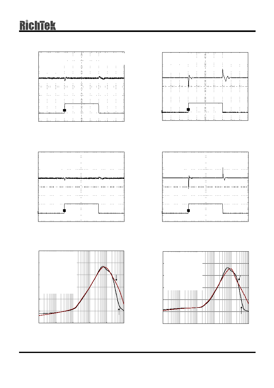
Typical Operating Charateristics
Short Circuit Current
0
0.2
0.4
0.6
0.8
1
1.2
1.4
0
2
4
6
8
10
Input/Output Differential (V)
S
h
o
r
t
C
i
rc
u
i
t
C
u
rre
n
t
(A
)
125
∞C
25
∞C
Temperature Stability
2.4
2.6
2.8
3
3.2
3.4
-50
-25
0
25
50
75
100
125
Temperature ()
O
u
t
p
u
t
V
o
l
t
ag
e (V
)
V
OUT
= 2.5V
V
OUT
= 3.3V
(
∞C)
Dropout Voltage (Vin-Vout)
0
0.2
0.4
0.6
0.8
1
0
100
200
300
400
500
ILoad(mA)
Dr
op
ou
t
V
o
l
t
ag
e (
V
)
V
OUT
= 3.3V
125
∞C
25
∞C
T
T
T
1 >
2 >
100
0
-100
-200
7
6
5
4
Line Transient Response
Time (100
µS/Div)
Out
put
V
o
l
t
age
Devi
at
i
on (
m
V
)
I
nput
V
o
l
t
age
Devi
at
i
on
(
V
)
C
OUT
= 10
µF Electrolytic
I
OUT
= 0.1A
V
OUT
= 3.3V
T
A
= 25
∞C
T
T
T
1 >
2 >
100
0
-100
-200
7
6
5
4
Line Transient Response
Time (100
µS/Div)
Out
put
V
o
l
t
age
Devi
at
i
on (
m
V
)
I
nput
V
o
l
t
age
Devi
at
i
on
(
V
)
C
OUT
= 10
µF Electrolytic
I
OUT
= 0.1A
V
OUT
= 2.5V
T
A
= 25
∞C
∞
Quiescient Current
0.00
0.02
0.04
0.06
0.08
0.10
0.12
0.14
-30
0
30
60
90
120
Temperature ( C)
I (
m
A
)
V
IN
= 5V