
RT9164
DS9164-13 September 2002
www.richtek.com
1
1A Fixed and Adjustable Low Dropout
Positive Voltage Regulators
General Description
The RT9164 series of high performance positive
voltage regulators is designed for applications
requiring low dropout performance at fully rated
current. Additionally, the RT9164 series provides
excellent regulation over variations in line and load.
Outstanding features include low dropout
performance at rated current, fast transient
response, internal current-limiting, and thermal-
shutdown protection of the output device. The
RT9164 series of three terminal regulators offers
fixed and adjustable voltage options available in
space-saving SOT-223, TO-252, and TO-263
packages.
Ordering Information
RT9164-
Features
Low Dropout Performance, 1.4V Max.
Full Current Rating Over Line and Temperature
Fast Transient Response
±
2% Output Voltage Accuracy
1.5V, 1.8V, 2.5V, 2.85V, 3.3V, and 3.5V
Fixed/Adjustable Output Voltage
SOT-223, TO-252, and TO-263 Packages
Applications
Active SCSI Termination
Low Voltage Microcontrollers
Switching Power Supply Post-Regulator
Pin Configurations
Part Number
Pin Configurations
RT9164-
CG
(Plastic SOT-223)
TOP VIEW
1. ADJ/GND
2. VOUT (TAB)
3. VIN
RT9164-
CL
(Plastic TO-252)
TOP VIEW
1. ADJ/GND
2. VOUT (TAB)
3. VIN
RT9164-
CLR
(Plastic TO-252)
TOP VIEW
1. VIN
2. GND (TAB)
3. VOUT
RT9164-
CM
(Plastic TO-263)
TOP VIEW
1. ADJ/GND
2. VOUT (TAB)
3. VIN
Operating temperature range
C: Commercial standard
Package type
G : SOT-223
L : TO-252 (DPAK)
LR : TO-252
M : TO-263
Output voltage
Default : Adjustable
15 : 1.5V
18 : 1.8V
25 : 2.5V
28 : 2.85V
33 : 3.3V
35 : 3.5V
1
2
3
1
2
3
1
2
3
1
2
3

RT9164
www.richtek.com
DS9164-13 September 2002
2
Absolute Maximum Ratings
Input Voltage
12V
Package Thermal Resistance
SOT-223,
JC
15
∞
C/W
SOT-223,
JA
(1)
60
∞
C/W
TO-252,
JC
15
∞
C/W
TO-252,
JA
(1)
56
∞
C/W
TO-263,
JC
8
∞
C/W
TO-263,
JA
(1)
19.4
∞
C/W
Operating Junction Temperature Range
0
∞
C to 125
∞
C
Storage Temperature Range
-
65
∞
C to 150
∞
C
Lead Temperature (Soldering, 10 sec.)
260
∞
C
Note: (1) Minimum pad size of 0.038 IN
2
Electrical Characteristics
(T
A
= 25
∞
C, unless otherwise specified)
Parameter
Symbol
Test Conditions
Min
Typ
Max Units
I
OUT
= 10mA, (V
IN
-V
OUT
) = 2V,
T
A
= 25
∞
C
1.231 1.256 1.281
V
Reference Voltage
(1)
RT9164
V
REF
10mA
<
I
OUT
<
1A,
1.4V
<
V
IN
-V
OUT
<
10V
1.218 1.256 1.294
V
I
OUT
= 10mA, V
IN
= 3.3V, T
J
= 25
∞
C
1.47
1.5
1.53
RT9164-15
0
<
I
OUT
<
1A, 3.3V
<
V
IN
<
10V
1.45
1.5
1.55
I
OUT
= 10mA, V
IN
= 3.3V, T
J
= 25
∞
C
1.78 1.815 1.85
RT9164-18
0
<
I
OUT
<
1A, 3.3V
<
V
IN
<
10V
1.76 1.815 1.87
I
OUT
= 10mA, V
IN
= 4.0V, T
J
= 25
∞
C
2.450 2.500 2.550
RT9164-25
0
<
I
OUT
<
1A, 4.0V
<
V
IN
<
10V
2.425 2.500 2.575
I
OUT
= 10mA, V
IN
= 4.25V, T
J
= 25
∞
C 2.790 2.850 2.910
RT9164-28
0
<
I
OUT
<
1A, 4.25V
<
V
IN
<
10V
2.765 2.850 2.936
I
OUT
= 10mA, V
IN
= 4.75V, T
J
= 25
∞
C 3.235 3.300 3.365
RT9164-33
0
<
I
OUT
<
1A, 4.75V
<
V
IN
<
10V
3.200 3.300 3.400
I
OUT
= 10mA, V
IN
= 5V, T
J
= 25
∞
C
3.430 3.500 3.570
Output Voltage
(1)
RT9164-35
V
OUT
0
<
I
OUT
<
1A, 5.0V
<
V
IN
<
10V
3.395 3.500 3.605
V
RT9164
I
OUT
= 10mA,
1.5V
V
IN
-V
OUT
10V
--
0.1
0.3
%
RT9164-15
I
OUT
= 0mA, 3.3V
V
IN
12V
--
1
6
mV
RT9164-18
I
OUT
= 0mA, 3.3V
V
IN
12V
--
1
6
mV
RT9164-25
I
OUT
= 0mA, 4.0V
V
IN
12V
--
1
6
mV
RT9164-28
I
OUT
= 0mA, 4.25V
V
IN
12V
--
1
6
mV
RT9164-33
I
OUT
= 0mA, 4.75V
V
IN
12V
--
1
6
mV
Line Regulation
(1)
RT9164-35
V
LINE
I
OUT
= 0mA, 5.0V
V
IN
12V
--
1
6
mV
To be continued
RT9164
DS9164-13 September 2002
www.richtek.com
3
Parameter
Symbol
Test Conditions
Min
Typ
Max Units
RT9164
(V
IN
-V
OUT
) = 3V, 0mA
I
OUT
1A
--
0.2
0.4
%
RT9164-15
V
IN
= 3.3V, 0
I
OUT
1A
--
1
10
mV
RT9164-18
V
IN
= 3.3V, 0
I
OUT
1A
--
1
10
mV
RT9164-25
V
IN
= 4.0V, 0
I
OUT
1A
--
1
10
mV
RT9164-28
V
IN
= 4.25V, 0
I
OUT
1A
--
1
10
mV
RT9164-33
V
IN
= 4.75V, 0
I
OUT
1A
--
1
10
mV
Load Regulation
(1)
RT9164-35
V
LOAD
V
IN
= 5.0V, 0
I
OUT
1A
--
1
15
mV
I
OUT
= 100mA
--
1.1
1.2
V
I
OUT
= 500mA
--
1.15
1.25
V
I
OUT
= 800mA
--
1.2
1.3
V
Dropout Voltage
(2)
V
DROP
I
OUT
= 1000mA
--
1.3
1.4
V
Current Limit
I
LIMIT
V
IN
= 5V
1000
--
2000
mA
Minimum Load Current RT9164
(V
IN
-V
OUT
) = 2V
--
5
10
mA
Quiescent Current
RT9164-XX I
Q
V
IN
= 5V
--
5
10
mA
Ripple Rejection
PSRR
f
RIPPLE
= 120Hz
,
(V
IN
- V
OUT
) = 2V, V
RIPPLE
= 1V
P-P
--
72
--
dB
Adjust Pin Current
I
ADJ
--
65
120
µ
A
Adjust Pin Current Change
I
ADJ
10mA
I
OUT
1A, V
IN
= 5V
--
0.2
5
µ
A
Notes:
(1) Low duty cycle pulse testing with Kelvin connections.
(2)
V
OUT
and
V
REF
= 2%.
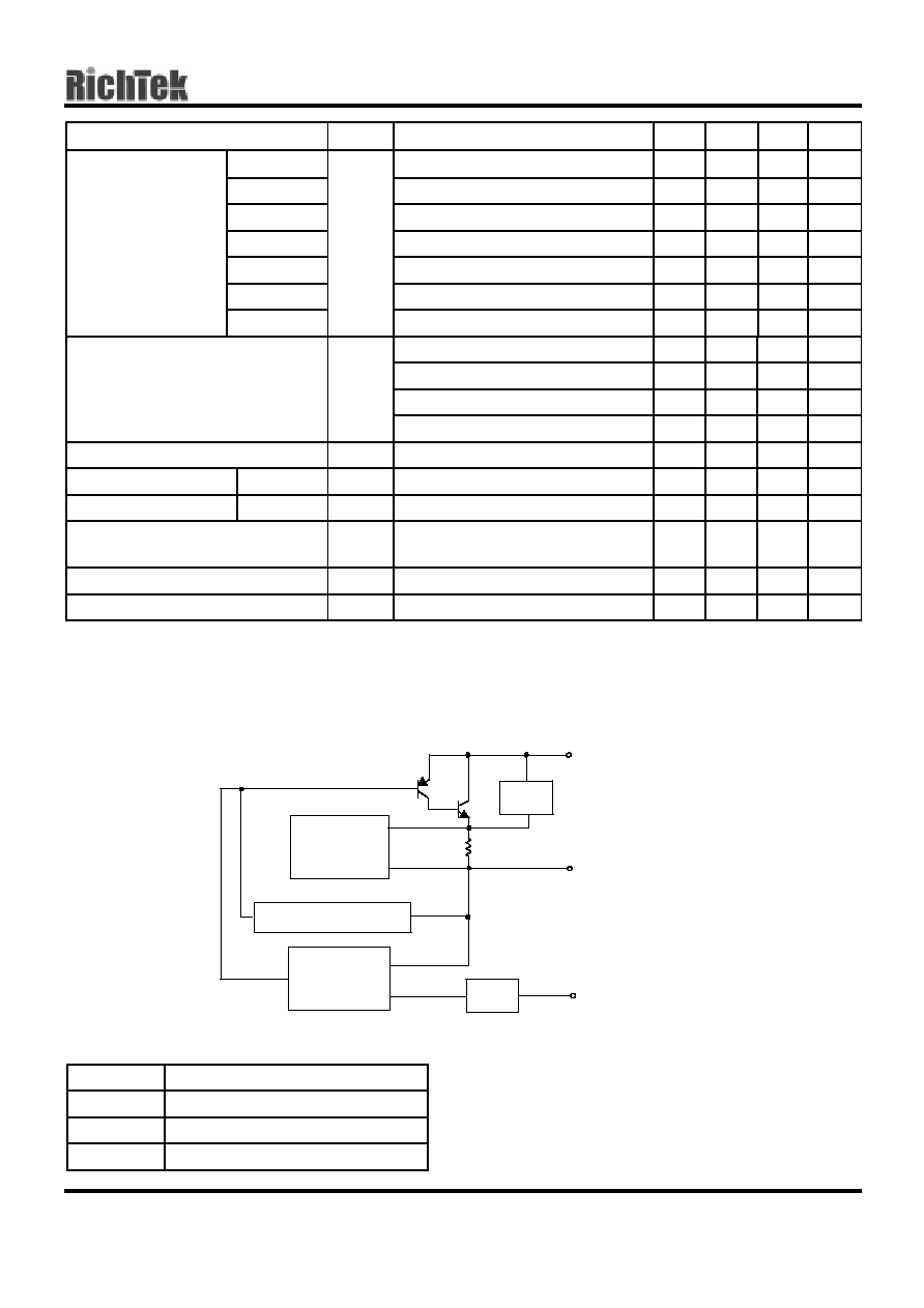
Function Block Diagram
Pin Description
Pin Name
Pin Function
ADJ/GND
Adjust Output or Ground
VOUT
Output Voltage
VIN
Power Input
S.O.A.
CURRENT
LIMITING
AMPLIFIER
THERMAL OVERLOAD
VOLTAGE
REGULATION
AMPLIFIER
V
REF
LIMIT
SENSE
VIN
VOUT
ADJ/GND

RT9164
www.richtek.com
DS9164-13 September 2002
4
Typical Application Circuit
Fig. 1 Adjustable Voltage Regulator
Fig. 2 Active SCSI Bus Terminator
Fig. 3 Fixed Voltage Regulator
RT9164
ADJ
VOUT
V
REF
R1
133
1%
R2
232
1%
V
OUT
= 3.45V
I
ADJ
V
IN
= 5V
+ C2
10
µ
F
Tantalum
+
C1
10
µ
F
(1) C1 needed if device is far from filter capacitors.
(2) C2 required for stability.
VIN
V
OUT
= V
REF
(1+ ) + I
ADJ
R
2
1
2
R
R
RT9164-28
+
22
µ
F
+
10
µ
F
VOUT
VIN
18 -27 Lines
GND
RT9164-33
+ C2
10
µ
F
Tantalum
+ C1
10
µ
F
I
Q
VOUT
VIN
V
IN
= 5V
V
OUT
3.3V
(1) C1 needed if device is far from filter capacitors.
(2) C2 required for stability.
GND

RT9164
DS9164-13 September 2002
www.richtek.com
5
Typical Operating Characteristics
Load Regulation
-0.35
-0.3
-0.25
-0.2
-0.15
-0.1
-0.05
0
-50
-25
0
25
50
75
100
125
Temperature (
C)
O
u
tput
V
o
l
t
age D
e
v
i
ati
on (
%
)
Load = 1A
∞
Adjust Pin Current
0
10
20
30
40
50
60
70
80
90
100
-50
-25
0
25
50
75
100
125
Temperature (
C)
A
d
j
u
s
t
P
i
n C
u
r
r
ent (
A
)
µ
∞
Dropout Voltage (V
IN
-V
OUT
)
0.0
0.2
0.4
0.6
0.8
1.0
1.2
0
200
400
600
800
Output Current (mA)
D
r
opout V
o
l
t
age (
V
)
T
J
= 25
∞
C
T
J
= 125
∞
C
Short-Circuit Current
0.0
0.5
1.0
1.5
2.0
2.5
0
2.5
5
7.5
10
Input/Output Differential (V)
S
hor
t
C
i
r
c
ui
t C
u
r
r
ent (
A
)
T
J
= 125
∞
C
T
J
= 25
∞
C
RT9164-ADJ Ripple Rejection
-100
-80
-60
-40
-20
0
Frequency (Hz)
R
i
pp
l
e
R
e
j
e
c
t
i
o
n(
dB
)
C
OUT
= 20
µ
F Tantalum
C
ADJ
= 22
µ
F Electrolytic
I
OUT
= 0.5A
10
100
1K
10K
100K
Ripple Rejection & Current
-100
-90
-80
-70
-60
-50
-40
-30
-20
I
LOAD
(mA)
R
i
pp
l
e
R
e
j
e
c
t
i
o
n(
dB
)
f
RIPPLE
= 20KHz
f
RIPPLE
= 120Hz
C
OUT
= 20
µ
F Tantalum
C
ADJ
= 22
µ
F Electrolytic
0 200 400 600 800