RT9169
DS9169-04 July 2002
www.richtek.com
1
100mA, 4
µ
A Quiescent Current CMOS LDO Regulator
General Description
The RT9169 series are 100mA ultra-low quiescent
current CMOS low dropout (LDO) regulator designed
for battery-powered equipments. The output voltages
range from 1.2V to 5V with 0.1V per step.
The other features include 4
µ
A ultra-low quiescent,
low dropout voltage, high output accuracy, current
limiting protection, and high ripple rejection ratio.
Ordering Information
RT9169-
Typical Application Circuit
Marking Information
For marking information, contact our sales
representative directly or through a RichTek
distributor located in your area, otherwise visit our
website for detail.
Features
Ultra-Low Quiescent Current: 4
µ
A
Low Dropout: 450mV at 100mA
Wide Operating Voltage Ranges: 2V~6V
Current Limiting Protection
Only 1
µ
F Output Capacitor Required for Stability
High Power Supply Rejection Ratio
Applications
Battery-Powered Equipment
Palmtops, Notebook Computers
Hand-held Instruments
PCMCIA Cards
Pin Configurations
Part Number
Pin Configurations
RT9169-
CZL
(Plastic TO-92)
TOP VIEW
1. VIN
2. GND
3.
VOUT
RT9169-
CZT
(Plastic TO-92)
TOP VIEW
1. VOUT
2. VIN
3.
GND
RT9169-
CX
(Plastic SOT-89)
TOP VIEW
1. GND
2. VIN (TAB)
3.
VOUT
RT9169-
CV
(Plastic SOT-23)
TOP VIEW
1. VOUT
2. GND
3.
VIN
RT9169-
CB
(Plastic SOT-25)
TOP VIEW
1. VIN
2. GND
3. EN
4. NC
5.
VOUT
Operating temperature range
C: Commercial standard
Package type
ZL : TO-92 L Type
ZT : TO-92 T Type
X : SOT-89
V : SOT-23
CB : SOT-25
Output voltage
12 : 1.2V
13 : 1.3V
:
49 : 4.9V
50 : 5.0V
V
OUT
RT9169
VOUT
C
OUT
1
µ
F
VIN
V
IN
C
IN
1
µ
F
GND
1
2
3
1
3
2
5
4
3
2
1
1 2 3
1 2 3

RT9169
www.richtek.com
DS9169-04 July 2002
2
Pin Description
Pin Name
Pin Function
VIN
Power Input
VOUT
Output Voltage
GND
Ground
EN
Chip Enable Control Input
Function Block Diagram
Absolute Maximum Ratings
Input Voltage
7V
Power Dissipation, P
D
@ T
A
= 25
∞
C
TO-92
0.6W
SOT-89
0.5W
SOT-23
0.25W
SOT-25
0.25W
Operating Junction Temperature Range
-40
∞
C to 125
∞
C
Storage Range
-65
∞
C to 150
∞
C
Package Thermal Resistance
TO-92,
JA
160
∞
C/W
SOT-89,
JC
100
∞
C/W
SOT-89,
JA
180
∞
C/W
SOT-23,
JA
250
∞
C/W
SOT-25,
JA
250
∞
C/W
Current
Limit
VIN
VOUT
GND
+
_
EN
RT9169
DS9169-04 July 2002
www.richtek.com
3
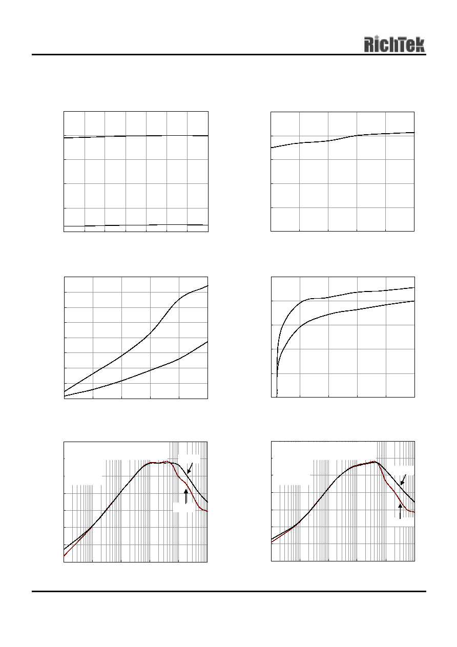
Electrical Characteristics
(V
IN
= 5.5V, C
IN
= 1
µ
F, C
OUT
= 1
µ
F, T
A
= 25
∞
C, unless otherwise specified)
Parameter
Symbol
Test Conditions
Min
Typ
Max
Units
Input Voltage Range
V
IN
2
--
6
V
Output Voltage Accuracy
V
OUT
I
L
= 1mA
-2
--
+2
%
Maximum Output Current
I
MAX
V
IN
= V
OUT
+ 0.6V, V
IN
3.6V
100
--
--
mA
Current Limit
I
LIMIT
I
L
= 100mA
150
250
--
mA
No Load
--
4
7
µ
A
GND Pin Current
I
G
I
OUT
= 100mA
4
10
µ
A
I
OUT
= 1mA, V
IN
3.6V
--
4
10
I
OUT
= 50mA, V
IN
3.6V
--
200
300
Dropout Voltage
V
DROP
I
OUT
= 100mA, V
IN
3.6V
--
450
600
mV
Line Regulation
V
LINE
V
IN
= (V
OUT
+ 0.3V) to 6V,
V
IN
3.6V, I
OUT
= 1mA
-0.2
--
+0.2
%/V
Load Regulation
V
LOAD
I
LOUT
= 0mA to 100mA
--
0.01
0.04
%/mA
Output Noise
e
NO
BW = 100Hz to 50KHz
C
OUT
= 10
µ
F
--
250
--
µ
V
Ripple Rejection
PSRR
F = 1KHz, C
OUT
= 1
µ
F
--
30
--
dB
Standby Current
RT9169-CB
EN = V
IN
--
0.1
1
µ
A
EN Threshold
0.6
1
2
V
Thermal Shutdown Protection
125
--
--
∞
C
Application Information
A 1
µ
F (or larger) capacitor is recommended between
VOUT and GND for stability. The part may oscillate
without the capacitor. Any type of capacitor can be
used, but not Aluminum electrolytes when operating
below ≠25
∞
C. The capacitance may be increased
without limit.
A 1
µ
F capacitor (or larger) should be placed between
VIN to GND.