 | –≠–ª–µ–∫—Ç—Ä–æ–Ω–Ω—ã–π –∫–æ–º–ø–æ–Ω–µ–Ω—Ç: R2061K | –°–∫–∞—á–∞—Ç—å:  PDF PDF  ZIP ZIP |

'03.07.15
12345
3 wire interface Real-Time Clock ICs
with Battery Backup switch-over Function
R2061 Series
12345
Rev.1.03 - 1 -
s
OUTLINE
The R2061 is a CMOS real-time clock IC connected to the CPU by three signal lines, CE, SCLK, and SIO, and
configured to perform serial transmission of time and calendar data to the CPU. Further, battery backup
switchover circuit and a voltage detector. The periodic interrupt circuit is configured to generate interrupt signals
with six selectable interrupts ranging from 0.5 seconds to 1 month. The 2 alarm interrupt circuits generate
interrupt signals at preset times. As the oscillation circuit is driven under constant voltage, fluctuation of the
oscillator frequency due to supply voltage is small, and the time keeping current is small (TYP. 0.4
µ
A at 3V). The
oscillation halt sensing circuit can be used to judge the validity of internal data in such events as power-on; The
supply voltage monitoring circuit is configured to record a drop in supply voltage below two selectable supply
voltage monitoring threshold settings. The oscillation adjustment circuit is intended to adjust time counts with high
precision by correcting deviations in the oscillation frequency of the crystal oscillator. Battery backup switchover
function is the automatic switchover circuit between a main power supply and a backup battery of primary or
secondary battery. Switchover is executed by monitoring the voltage of a main power supply, therefore the voltage
of a backup battery voltage is not relevant. This model comes in an ultra-compact FFP12 (Height 1.00mm,
2.0mm
◊
2.0mm).
s
FEATURES
q
Minimum Timekeeping supply voltage Typ. 0.75V (Max. 1.00V); VDD pin
q
Low power consumption
0.4
µ
A TYP (1.0
µ
A MAX.)
at VDD=3V
q
Built-in Backup switchover circuit (can be used for a primary battery, a secondary battery, or an electric double
layer capacitor)
q
Three signal lines (CE, SCLK, and SIO) required for connection to the CPU.
(Maximum clock frequency of 1MHz (with VCC = 3V) )
q
Time counters (counting hours, minutes, and seconds) and calendar counters (counting years, months, days,
and weeks) (in BCD format)
q
Interrupt circuit configured to generate interrupt signals (with interrupts ranging from 0.5 seconds to 1 month) to
the CPU and provided with an interrupt flag and an interrupt halt
q
2 alarm interrupt circuits (Alarm_W for week, hour, and minute alarm settings and Alarm_D for hour and minute
alarm settings)
q
Built-in voltage detector with delay
q
With Power-on flag to prove that the power supply starts from 0V
q
Supply voltage monitoring circuit with two supply voltage monitoring threshold settings
q
Automatic identification of leap years up to the year 2099
q
Selectable 12-hour and 24-hour mode settings
q
Built-in oscillation stabilization capacitors (CG and CD)
q
High precision oscillation adjustment circuit
q
CMOS process
q
Ultra-compact FFP12
s
PIN CONFIGURATION
VDD
VCC
SIO
VSS
10
11
12
1
2
3
4
TOP VIEW
R2061K(FFP12)
7
VSB
CE
SCL
K
/V
DCC
CIN
5
6
9
8
OS
CIN
OS
COUT
/INT
R

R2061 Series
12345
Rev.1.03 - 2 -
s
BLOCK DIAGRAM
OSCOUT
VSS
VDD
/INTR
CPU POWER
SUPPLY
OSCIN
VCC
VSB
CPU
REAL
TIME
CLOCK
SCLK
CE
C3
BATTERY
VOLTAGE
MONITOR
/VDCC
VOLTAGE
DETECTOR
SW1
SW2
SIO
C2
R1
LE
V
E
L
SH
IF
TER
DELAY
CIN
VOLTAGE
REFERENCE
C1
s
SELECTION GUIDE
In the R2061xxx Series, output voltage and options can be designated.
Part Number is designated as follows:
R2061K01-E2
Part Number
R2061abb-cc
Code Description
a
Designation of the package.
K: FFP12
S: SSOP16
bb
Serial number of Voltage detector setting etc.
cc
Designation of the taping type. Only E2 is available.

R2061 Series
12345
Rev.1.03 - 3 -
s
PIN DESCRIPTION
Symbol Item
Description
CE Chip
enable
Input
The CE pin is used for interfacing with the CPU. Should be held high to
allow access to the CPU. Incorporates a pull-down resistor. Should be
held low or open when the CPU is powered off. Allows a maximum input
voltage of 5.5 volts regardless of supply voltage.
SCLK Serial
Clock Input
The SCLK pin is used to input clock pulses synchronizing the input and
output of data to and from the SIO pin. Allows a maximum input voltage of
5.5 volts regardless of supply voltage.
SIO Serial
Input / Output
The SIO pin is used to input or output data intended for writing or reading in
synchronization with the SCLK pin.
/INTR Interrupt
Output
The /INTR pin is used to output alarm interrupt (Alarm_W) and alarm
interrupt (Alarm_D) and output periodic interrupt signals to the CPU signals.
Disabled at power-on from 0V. Nch. open drain output.
VCC Main
Battery
input
Supply power to the IC.
VSB Power
Supply
Input for Backup
Battery
Connect a primary battery for backup. Normally, power is supplied from VCC
to the IC. If VCC level is equal or less than ≠VDET1, power is supplied from
this pin.
OSCIN
OSCOUT
Oscillation
Circuit
Input / Output
The OSCIN and OSCOUT pins are used to connect the 32.768-kHz crystal
oscillator (with all other oscillation circuit components built into the R2061K
series).
VDD
Positive Power
Supply Input
The VDD pin is connected to the power supply. Connect a capacitor as much
as 0.1
µ
F between VDD and VSS. In the case of using a secondary battery,
connecting the secondary battery to this pin is possible.
/VDCC VCC
Power
Supply Monitoring
Result Output
While monitoring VCC Power supply, if the voltage is equal or lower than
≠VDET1, this output level is "L". When /VDCC becomes "L", SW1 turns off
and SW2 turns on. As a result, power is supplied from VSB pin to the
internal real time clock. When VCC is equal to +VDET1 or more, SW1 turns
on and SW2 turns off. After t DELAY passed, /VDCC output becomes off, or
"H".
Nch Open-drain output.
CIN
Noise Bypass Pin
To stabilize the internal reference, connect a capacitor as much as 0.1uF
between this pin and VSS.
VSS Negative
Power
Sup Supply Input
The VSS pin is grounded.

R2061 Series
12345
Rev.1.03 - 4 -
s
ABSOLUTE MAXIMUM RATINGS
(VSS=0V)
Symbol Item
Pin
Name
Description
Unit
VCC
Supply Voltage 1
VCC
-0.3 to +6.5
V
VDD
Supply Voltage 2
VDD
-0.3 to +6.5
V
VSB
Supply Voltage 3
VSB
-0.3 to +6.5
V
Input Voltage 1
CE, SCLK
-0.3 to +6.5
V
Input Voltage 2
SIO
-0.3 to VCC+0.3
V
VI
Input Voltage 3
CIN
-0.3 to VDD+0.3
V
Output Voltage 1
/INTR, /VDCC
-0.3 to +6.5
V
VO
Output Voltage 2
SIO
-0.3 to VCC+0.3
V
IOUT
Maximum Output Current
VDD
10
mA
PD Power
Dissipation Topt = 25
∞
C
300 mW
Topt
Operating Temperature
-40 to +85
∞
C
Tstg
Storage Temperature
-55 to +125
∞
C
s
RECOMMENDED OPERATING CONDITIONS
(VSS=0V,
Topt=-40
to
+85
∞
C)
Symbol Item
Pin
Name
Min,
Typ. Max. Unit
Vaccess Supply
Voltage
VCC power supply
voltage for interfacing
with CPU
-VDET1
5.5 V
VCLK Minimum
Timekeeping
Voltage
CGout,CDout=0pF
*2), *3)
0.75
1.00
V
fXT Oscillation
Frequency
32.768
kHz
VPUP
Pull-up Voltage
/INTR, /VDCC
5.5
V
*1) -VDET1 in Vaccess specification is guaranteed by design.
*2) CGout is connected between OSCIN and VSS, CDout is connected between OSCOUT and VSS.
R2061 series incorporates the capacitors between OSCIN and VSS, between OSCOUT and VSS.
Then normally, CGout and CDout are not necessary.
*3) Crystal oscillator: CL=6-8pF, R1=30K
R2061 Series
12345
Rev.1.03 - 5 -
s
DC ELECTRICAL CHARACTERISTICS (PRELIMINARY)
q
R2061K01
(Unless otherwise specified: VSS=0V,VSB=3.0V, VCC=2.0V, 0.1uF between VDD and VSS, CIN and VSS,
Topt=-40 to +85
∞
C)
Symbol Item
Pin
Name Conditions
Min. Typ. Max. Unit
VIH1
"H" Input Voltage 1
CE, SCLK
0.8x
VCC
5.5
VIH2
"H" Input Voltage 2
SIO
0.8x
VCC
VCC+
0.3
VIL
"L" Input Voltage
CE, SCLK
SIO
-0.3
0.2x
VCC
V
IOH "H"
Output
Current
SIO VOH=VCC-0.5V -0.5
mA
IOL1
"L" Output Current 1
SIO
0.5
IOL2
"L" Output Current 2
/INTR
VOL=0.4V
2.0
IOL3
"L" Output Current 3
/VDCC
VDD,VSB,VCC=1.4V
VOL=0.4V
0.2
mA
IIL Input
Leakage
Current
SCLK
VI=5.5V or VSS
-1.0
1.0
µ
A
RDNCE Pull-down
Input
register
CE
40
120
400
k
IOZ1 Output
Off-state
Current 1
SIO
VO=5.5V or VSS
-1.0
1.0
µ
A
IOZ2 Output
Off-state
Current 2
/INTR,
/VDCC
VO=5.5V or VSS
-1.0
1.0
µ
A
ISB
Time Keeping Current
at Backup mode
VSB VCC=0V,
VSB=3.0V,
VDD, Output=OPEN
0.4
1.0
µ
A
ISBL
Leakage Current of
Backup pin at
VCC_on
VSB VCC=3.0V,
VSB=5.5V or 0V,
VDD, Output=OPEN
-1.0
1.0
µ
A
VDETH Supply
Voltage
Monitoring Voltage "H"
VSB
Topt=25
∞
C
1.90 2.10 2.30 V
VDETL Supply
Voltage
Monitoring Voltage "L"
VDD
Topt=25
∞
C
1.20 1.35 1.50 V
-VDET1 Detector
Threshold
Voltage
(falling edge of VCC)
VCC
Topt=25
∞
C
1.657 1.700 1.743 V
+VDET1 Detector
Released
Voltage (rising edge of
VCC)
VCC
Topt=25
∞
C
1.731 1.785 1.839 V
VDET
Topt
Detector Threshold
and Released Voltage
Temperature
coefficient
VCC,
VSB
Topt=-40 to 85
∞
C
*1)
±
100
ppm
/
∞
C
VDD
OUT1
VDD Output
Voltage 1
VDD
Topt=25
∞
C, VCC=2.0V,
Iout=0.5mA
VCC-
0.12
VCC-
0.04
V
VDD
OUT2
VDD Output
Voltage 2
VDD
Topt=25
∞
C, VCC=1.4V,
VSB=3.0V, Iout=0.1mA
VSB-
0.08
VSB-
0.02
V
CG Internal
Oscillation
Capacitance 1
OSCIN
10
CD Internal
Oscillation
Capacitance 2
OSCOUT
10
pF
*1) Guaranteed by design.
R2061 Series
12345
Rev.1.03 - 6 -
s
AC ELECTRICAL CHARACTERISTICS
Unless otherwise specified: VSS=0V,Topt=-40 to +85
∞
C
Input and Output Conditions: VIH=0.8
◊
VCC,VIL=0.2
◊
VCC,VOH=0.8
◊
VCC,VOL=0.2
◊
VCC,CL=50pF
VDD
1.7V *1)
Sym
-bol
Item
Condi-
Tions
Min. Typ. Max.
Unit
t
CES
CE
Set-up
Time
400
ns
t
CEH
CE
Hold
Time
400
ns
t
CR
CE
Recovery
Time
62
µ
s
f
SCLK
SCLK Clock Frequency
1.0
MHz
t
CKH
SCLK Clock "H" Time
400
ns
t
CKL
SCLK Clock "L" Time
400
ns
t
CKS
SCLK
Set-up
Time 200
ns
t
RD
Data Output Delay
Time
300
ns
t
RZ
Data
Output
Floating
Time
300
ns
t
CEZ
Data Output Delay
Time After Falling of CE
300
ns
t
DS
Input Data Set-up Time
200
ns
t
DH
Input Data Hold Time
200
ns
t
DELAY
Output Delay Time of
Voltage Detector
Time
Keeping
100 105 110 ms
*1) VCC voltage interfacing with CPU is defined by Vaccess (P.4
s
RECOMMENDED OPERATING
CONDITIONS)
*) For reading/writing timing, see "P.24
s
Interfacing with the CPU
q
Considerations in Reading and Writing Time
Data under special condition".
SCLK
t
CES
SIO(OUT)
SIO(IN)
CE
t
RD
t
CKL
t
CEZ
t
DS
t
DH
t
RD
t
CEH
t
CKH
t
CK
S
t
CR
t
RZ
/VDCC
VCC
t
DELAY
+VDET1

R2061 Series
12345
Rev.1.03 - 7 -
s
PACKAGE DIMENSIONS
q
R2061Kxx
9 7
6
4
3
1
10
12
1PIN INDEX
2.0
±
0.1
0.2
±
0.15
0.35
2.0
±
0.1
2PIN INDEX
0.5
0.3
±
0.15
0.103
0.25
0.35
1.0Max
0.27
±
0.15
(BOTTOM VIEW)
0.5
0.05
0.17
±
0.1
q
TAPING SPECIFICATION
The R2061 Series have one designated taping direction. The product designation for the taping components
is "R2061S/Kxx-E2".

R2061 Series
12345
Rev.1.03 - 8 -
s
GENERAL DESCRIPTION
q
Battery Backup Switchover Function
The R2061 Series have two power supply input, or VCC and VSB. With monitoring VCC pin input voltage, which
voltage between the two is supplied to the internal power supply is decided.
Refer to the next table to see the state of the backup battery and internal power supply's state of the IC by each
condition.
VCC
VDET1 VCC
<
VDET1
VCC
RTC, VDD
/VDCC=OFF(H)
VSB
RTC, VDD
/VDCC=L
As a backup battery, not only a primary battery such as CR2025, LR44, or a secondary battery such as ML614,
TC616, but also an electric double layered capacitor or an aluminum capacitor can be used. Switchover point is
judged with the voltage of the main power (VCC), therefore, if the backup voltage is higher than main supply
voltage, switchover can be realized without extra load to the backup power supply.
VDD
VSB
VCC
VSS
0.1
µ
F
CPU Power
Supply
The case of back-up by
primary battery
CR2025
etc.
VSB
VDD
VCC
VSS
0.1
µ
F
CPU power
supply
ML614
etc.
The case of back-up by
capacitor or secondary battery
(Charging voltage is equal to CPU
power supply voltage)
VSB
VDD
VCC
VSS
0.1
µ
F
CPU power
supply
(3V)
5V
Double layer
capacitor
etc.
The case of back-up by
capacitor or secondary battery
(Charging voltage is not equal to
CPU power supply voltage)
q
Interface with CPU
The R2061 is connected to the CPU by three signal lines CE (Chip Enable), SCLK (Serial Clock), and SIO (Serial
Input / Output), through which it reads and writes data from and to the CPU. The CPU can be accessed when
the CE pin is held high. Access clock pulses have a maximum frequency of 1 MHz, allowing high-speed data
transfer to the CPU. VCC falls down under -VDET1, the R2061 stops accessing with CPU.
q
Clock and Calendar Function
The R2061 reads and writes time data from and to the CPU in units ranging from seconds to the last two digits of
the calendar year. The calendar year will automatically be identified as a leap year when its last two digits are a
multiple of 4. Consequently, leap years up to the year 2099 can automatically be identified as such.
*) The year 2000 is a leap year while the year 2100 is not a leap year.

R2061 Series
12345
Rev.1.03 - 9 -
q
Alarm Function
The R2061 incorporates the alarm interrupt circuit configured to generate interrupt signals to the CPU at preset
times. The alarm interrupt circuit allows two types of alarm settings specified by the Alarm_W registers and the
Alarm_D registers. The Alarm_W registers allow week, hour, and minute alarm settings including combinations of
multiple day-of-week settings such as "Monday, Wednesday, and Friday" and "Saturday and Sunday". The
Alarm_D registers allow hour and minute alarm settings. The Alarm_W outputs from /INTR pin, and the Alarm_D
outputs also from /INTR pin. Each alarm function can be checked from the CPU by using a polling function.
q
High-precision Oscillation Adjustment Function
The R2061 has built-in oscillation stabilization capacitors (CG and CD), that can be connected to an external
crystal oscillator to configure an oscillation circuit. Two kinds of accuracy for this function are alternatives. To
correct deviations in the oscillator frequency of the crystal, the oscillation adjustment circuit is configured to allow
correction of a time count gain or loss (up to
±
1.5ppm or
±
0.5ppm at 25
∞
C) from the CPU. The maximum range is
approximately
±
189ppm (or
±
63ppm) in increments of approximately 3ppm (or 1ppm). Such oscillation
frequency adjustment in each system has the following advantages:
* Allows timekeeping with much higher precision than conventional RTCs while using a crystal oscillator with
a wide range of precision variations.
* Corrects seasonal frequency deviations through seasonal oscillation adjustment.
* Allows timekeeping with higher precision particularly with a temperature sensing function out of RTC, through
oscillation adjustment in tune with temperature fluctuations.
q
Power-on Reset, Oscillation Halt Sensing Function and Supply Voltage Monitoring Function
The R2061 has 3 power supply pins (VCC, VSB, VDD), among them, VCC pin and VDD pin have monitoring
function of supply voltage. VCC power supply monitoring circuit makes /VDCC pin "L" when VCC power supply
pin becomes equal or lower than ≠VDET1. At the power-on of VDD, this circuit makes /VDCC pin turn off, or "H"
after the delay time, tDELAY from when the VCC power supply pin becomes equal or more than +VDET1.
The R2061 incorporates an oscillation halt sensing circuit equipped with internal registers configured to record
any past oscillation halt, the oscillation halt sensing circuit, VDD monitoring flag, and power-on reset flag are
useful for judging the validity of time data.
Power on reset function reset the control resisters when the system is powered on from 0V. At the same time, the
fact is memorized to the resister as a flag, thereby identifying whether they are powered on from 0V or battery
backed-up.
The R2061 also incorporates a supply voltage monitoring circuit equipped with internal registers configured to
record any drop in supply voltage below a certain threshold value. Supply voltage monitoring threshold settings
can be selected between 2.1V and 1.35V through internal register settings. The sampling rate is normally 1s. The
oscillation halt sensing circuit is configured to confirm the established invalidation of time data in contrast to the
supply voltage monitoring circuit intended to confirm the potential invalidation of time data. Further, the supply
voltage monitoring circuit can be applied to battery supply voltage monitoring.
q
Periodic Interrupt Function
The R2061 incorporates the periodic interrupt circuit configured to generate periodic interrupt signals aside from
interrupt signals generated by the periodic interrupt circuit for output from the /INTR pin. Periodic interrupt signals
have five selectable frequency settings of 2 Hz (once per 0.5 seconds), 1 Hz (once per 1 second), 1/60 Hz (once
per 1 minute), 1/3600 Hz (once per 1 hour), and monthly (the first day of every month). Further, periodic
interrupt signals also have two selectable waveforms, a normal pulse form (with a frequency of 2 Hz or 1 Hz) and
special form adapted to interruption from the CPU in the level mode (with second, minute, hour, and month
interrupts). The condition of periodic interrupt signals can be monitored with using a polling function.

R2061 Series
12345
Rev.1.03 - 10 -
s
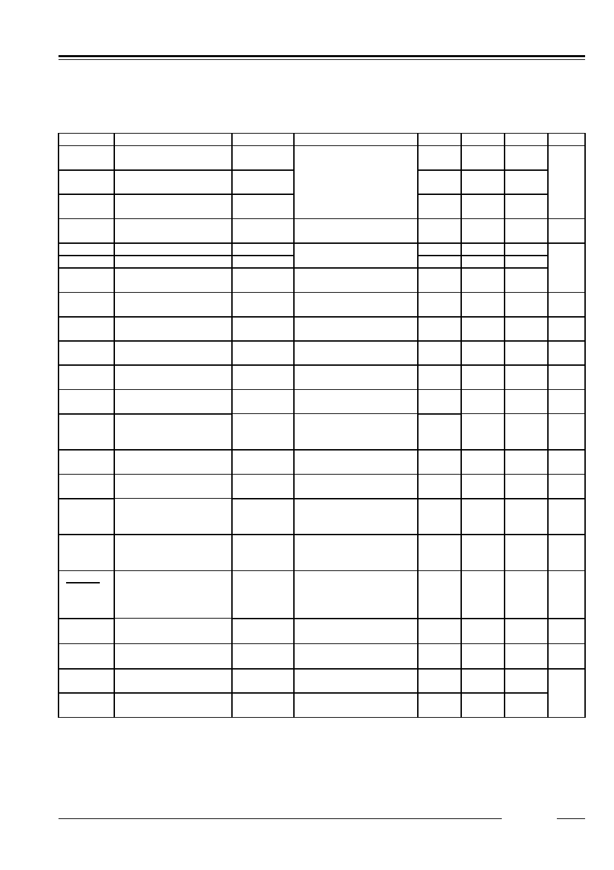
Address Mapping
Address
Register Name
D a t a
A3A2A1A0
D7 D6 D5 D4 D3 D2
D1 D0
0 0 0 0 0
Second Counter
-
*2)
S40 S20 S10 S8 S4 S2 S1
1 0 0 0 1
Minute Counter
-
M40
M20
M10
M8
M4
M2
M1
2 0 0 1 0
Hour Counter
-
-
H20
P
/A
H10 H8 H4
H2 H1
3
0
0
1
1 Day-of-week
Counter
- - - - - W4
W2
W1
4 0 1 0 0
Day-of-month Counter
-
-
D20
D10
D8
D4
D2
D1
5 0 1 0 1
Month Counter and
Century Bit
/19
20
- - MO10
MO8
MO4
MO2
MO1
6 0 1 1 0
Year Counter
Y80
Y40
Y20
Y10
Y8
Y4
Y2
Y1
7 0 1 1 1
Oscillation Adjustment
Register *3)
DEV
*4)
F6 F5 F4 F3 F2
F1 F0
8 1 0 0 0
Alarm_W
(Minute Register)
-
WM40
WM20
WM10
WM8
WM4
WM2 WM1
9 1 0 0 1
Alarm_W
(Hour Register)
- -
WH20
WP
/ A
WH1
0
WH8 WH
4
WH2 WH
1
A 1 0 1 0
Alarm_W
(Day-of-week
Register)
-
WW6 WW5 WW4 WW3 WW2 WW1 WW0
B 1 0 1 1
Alarm_D
(Minute Register)
-
DM40
DM20
DM10
DM8 DM4
DM2 DM1
C 1 1 0 0
Alarm_D
(Hour Register)
- - DH20
DP
/A
DH10 DH8 DH4
DH2 DH1
D
1
1
0
1
- - - - - -
- -
E 1 1 1 0
Control Register 1 *3) WALE
DALE
/12
24
SCRA
TCH2
TEST CT2 CT1 CT0
F 1 1 1 1
Control Register 2 *3)
VDSL
VDET
/XST
PON
*5)
SCRA
TCH1
CTFG WAFG DAF
G
Notes:
* 1) All the data listed above accept both reading and writing.
* 2) The data marked with "-" is invalid for writing and reset to 0 for reading.
* 3) When the PON bit is set to 1 in Control Register 2, all the bits are reset to 0 in Oscillation Adjustment
Register, Control Register 1 and Control Register 2 excluding the /XST bit.
* 4) When DEV=0, the oscillation adjustment circuit is configured to allow correction of a time count gain or
loss up to
±
1.5ppm.
When DEV=1, the oscillation adjustment circuit is configured to allow correction of a time count gain or
loss up to or
±
0.5ppm.
* 5) PON is a power-on-reset flag.

R2061 Series
12345
Rev.1.03 - 11 -
s
Register Settings
q
Control Register 1 (ADDRESS Eh)
D7 D6 D5 D4 D3 D2 D1 D0
WALE DALE /12
24
SCRA
TCH2
TEST
CT2 CT1 CT0 (For
Writing)
WALE DALE /12
24
SCRA
TCH2
TEST
CT2 CT1 CT0 (For
Reading)
0 0 0 0 0 0 0 0 Default
Settings
*)
*) Default settings: Default value means read / written values when the PON bit is set to "1" due to VDD
power-on from 0 volts.
(1) WALE, DALE Alarm_W Enable Bit, Alarm_D Enable Bit
WALE,DALE Description
0
Disabling the alarm interrupt circuit (under the control of the settings
of the Alarm_W registers and the Alarm_D registers).
(Default)
1
Enabling the alarm interrupt circuit (under the control of the settings
of the Alarm_W registers and the Alarm_D registers)
(2) /12
24
/12-24-hour Mode Selection Bit
/12
24
Description
0
Selecting the 12-hour mode with a.m. and p.m. indications.
(Default)
1
Selecting the 24-hour mode
Setting the /12
24 bit to 0 and 1 specifies the 12-hour mode and the 24-hour mode, respectively.
24-hour mode
12-hour mode
24-hour mode
12-hour mode
00 12
(AM12)
12 32
(PM12)
01
01 (AM 1)
13
21 (PM 1)
02
02 (AM 2)
14
22 (PM 2)
03
03 (AM 3)
15
23 (PM 3)
04
04 (AM 4)
16
24 (PM 4)
05
05 (AM 5)
17
25 (PM 5)
06
06 (AM 6)
18
26 (PM 6)
07
07 (AM 7)
19
27 (PM 7)
08
08 (AM 8)
20
28 (PM 8)
09
09 (AM 9)
21
29 (PM 9)
10 10
(AM10)
22 30
(PM10)
11
11 (AM11)
23
31 (PM11)
Setting the /12
24 bit should precede writing time data
(3) SCRATCH2
Scratch Bit 2
SCRATCH2 Description
0
(Default)
1
The SCRATCH2 bit is intended for scratching and accepts the reading and writing of 0 and 1.
The SCRATCH2 bit will be set to 0 when the PON bit is set to 1 in the Control Register 1.
(4) TEST
Test Bit
TEST Description
0 Normal
operation
mode.
(Default)
1 Test
mode.
The TEST bit is used only for testing in the factory and should normally be set to 0.
R2061 Series
12345
Rev.1.03 - 12 -
(5) CT2,CT1, and CT0
Periodic Interrupt Selection Bits
Description
CT2 CT1 CT0
Wave form
mode
Interrupt Cycle and Falling Timing
0 0 0 -
OFF(H)
(Default)
0 0 1 -
Fixed
at
"L"
0 1 0 Pulse
Mode
*1)
2Hz(Duty50%)
0 1 1 Pulse
Mode
*1)
1Hz(Duty50%)
1 0 0 Level
Mode
*2)
Once per 1 second (Synchronized with
second counter increment)
1 0 1 Level
Mode
*2)
Once per 1 minute (at 00 seconds of
every minute)
1 1 0 Level
Mode
*2)
Once per hour (at 00 minutes and 00
seconds of every hour)
1 1 1 Level
Mode
*2)
Once per month (at 00 hours, 00
minutes,
and 00 seconds of first day of every
month)
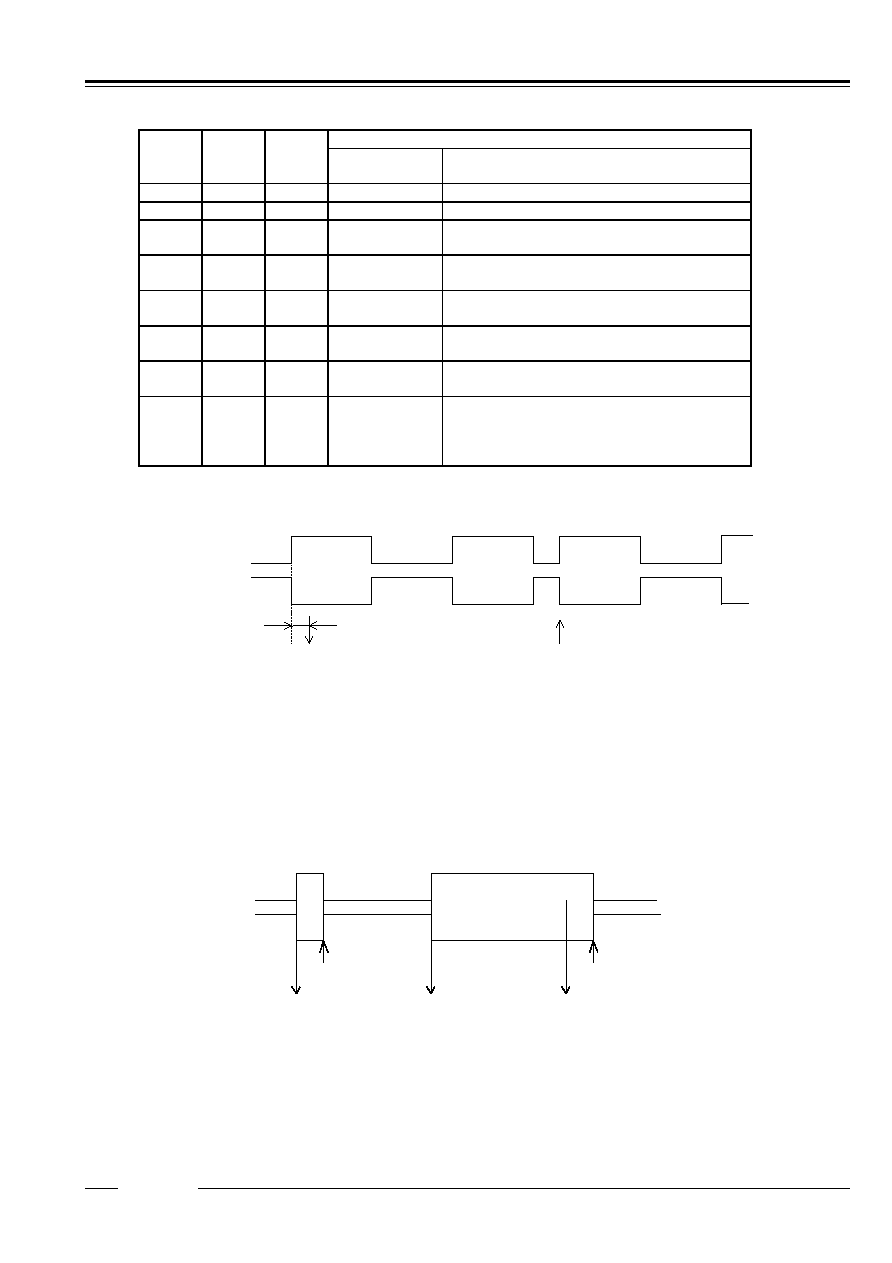
* 1) Pulse Mode: 2-Hz and 1-Hz clock pulses are output in synchronization with the increment of the second
counter as illustrated in the timing chart below.
/INTR Pin
Rewriting of the second counter
CTFG Bit
Approx. 92
µ
s
(Increment of second counter)
In the pulse mode, the increment of the second counter is delayed by approximately 92
µ
s from the
falling edge of clock pulses. Consequently, time readings immediately after the falling edge of clock
pulses may appear to lag behind the time counts of the real-time clocks by approximately 1 second.
Rewriting the second counter will reset the other time counters of less than 1 second, driving the
/INTR pin low.
* 2) Level Mode: Periodic interrupt signals are output with selectable interrupt cycle settings of 1 second, 1
minute, 1 hour, and 1 month. The increment of the second counter is synchronized with the falling
edge of periodic interrupt signals. For example, periodic interrupt signals with an interrupt cycle
setting of 1 second are output in synchronization with the increment of the second counter as
illustrated in the timing chart below.
(Increment of
second counter)
Setting CTFG bit to 0
Setting CTFG bit to 0
(Increment of
second counter)
(Increment of
second counter)
CTFG Bit
/INTR Pin
*1), *2) When the oscillation adjustment circuit is used, the interrupt cycle will fluctuate once per 20sec. or
60sec. as follows:
Pulse Mode: The "L" period of output pulses will increment or decrement by a maximum of
±
3.784 ms. For
example, 1-Hz clock pulses will have a duty cycle of 50
±
0.3784%.
Level Mode: A periodic interrupt cycle of 1 second will increment or decrement by a maximum of
±
3.784 ms.
R2061 Series
12345
Rev.1.03 - 13 -
q
Control Register 2 (Address Fh)
D7 D6 D5 D4 D3 D2 D1 D0
VDSL VDET /XST PON SCRA
TCH1
CTFG WAFG DAFG (For
Writing)
VDSL VDET /XST PON SCRA
TCH1
CTFG WAFG DAFG (For
Reading)
0 0
Indefinite
1 0 0 0 0 Default
Settings
*)
*) Default settings: Default value means read / written values when the PON bit is set to "1" due to VDD
power-on from 0 volts.
(1) VDSL
VDD Supply Voltage Monitoring Threshold Selection Bit
VDSL Description
0
Selecting the VDD supply voltage monitoring threshold setting of 2.1v.
(Default)
1
Selecting the VDD supply voltage monitoring threshold setting of
1.35v.
The VDSL bit is intended to select the VDD supply voltage monitoring threshold settings.
(2) VDET
Supply Voltage Monitoring Result Indication Bit
VDET Description
0
Indicating supply voltage above the supply voltage monitoring
threshold settings.
(Default)
1
Indicating supply voltage below the supply voltage monitoring
threshold settings.
Once the VDET bit is set to 1, the supply voltage monitoring circuit will be disabled while the VDET bit will
hold the setting of 1. The VDET bit accepts only the writing of 0, which restarts the supply voltage
monitoring circuit. Conversely, setting the VDET bit to 1 causes no event.
(3) /XST
Oscillation Halt Sensing Monitor Bit
/XST Description
0
Sensing a halt of oscillation
1
Sensing a normal condition of oscillation
The /XST accepts the reading and writing of 0 and 1. The /XST bit will be set to 0 when the oscillation halt
sensing. The /XST bit will hold 0 even after the restart of oscillation.
(4) PON
Power-on-reset Flag Bit
PON Description
0 Normal
condition
1
Detecting VDD power-on -reset
(Default)
The PON bit is for sensing power-on reset condition.
*
The PON bit will be set to 1 when VDD power-on from 0 volts. The PON bit will hold the setting of 1
even after power-on.
*
When the PON bit is set to 1, all bits will be reset to 0, in the Oscillation Adjustment Register, Control
Register 1, and Control Register 2, except /XST and PON. As a result, /INTR pin stops outputting.
*
The PON bit accepts only the writing of 0. Conversely, setting the PON bit to 1 causes no event.
(5) SCRATCH1
Scratch Bit 1
SCRATCH1 Description
0
(Default)
1
The SCRATCH1 bit is intended for scratching and accepts the reading and writing of 0 and 1. The
SCRATCH1 bit will be set to 0 when the PON bit is set to 1 in the Control Register 2.

R2061 Series
12345
Rev.1.03 - 14 -
(6) CTFG
Periodic Interrupt Flag Bit
CTFG Description
0
Periodic interrupt output = "H"
(Default)
1
Periodic interrupt output = "L"
The CTFG bit is set to 1 when the periodic interrupt signals are output from the /INTR pin ("L"). The CTFG
bit accepts only the writing of 0 in the level mode, which disables ("H") the /INTR pin until it is enabled ("L")
again in the next interrupt cycle. Conversely, setting the CTFG bit to 1 causes no event.
(7) WAFG,DAFG
Alarm_W Flag Bit and Alarm_D Flag Bit
WAFG,DAFG Description
0
Indicating a mismatch between current time and preset alarm time
(Default)
1
Indicating a match between current time and preset alarm time
The WAFG and DAFG bits are valid only when the WALE and DALE have the setting of 1, which is caused
approximately 61
µ
s after any match between current time and preset alarm time specified by the Alarm_W
registers and the Alarm_D registers. The WAFG (DAFG) bit accepts only the writing of 0. /INTR pin
outputs off ("H") when this bit is set to 0. And /INTR pin outputs "L" again at the next preset alarm time.
Conversely, setting the WAFG and DAFG bits to 1 causes no event. The WAFG and DAFG bits will have
the reading of 0 when the alarm interrupt circuit is disabled with the WALE and DALE bits set to 0. The
settings of the WAFG and DAFG bits are synchronized with the output of the /INTR pin as shown in the
timing chart below.
/INTR Pin
Writing of 0 to
WAFG(DAFG) bit
WAFG(DAFG) Bit
(Match between
current time and
preset
alarm
ti
)
Approx. 61
µ
s
Approx. 61
µ
s
Writing of 0 to
WAFG(DAFG) bit
(Match between
current time and
preset
alarm
ti
)
(Match between
current time and
preset
alarm
ti
)
R2061 Series
12345
Rev.1.03 - 15 -
q
Time Counter (Address 0-2h)
Second Counter (Address 0h)
D7 D6 D5 D4 D3 D2 D1 D0
-
S40 S20 S10 S8 S4 S2 S1 (For
Writing)
0
S40 S20 S10 S8 S4 S2 S1 (For
Reading)
0
Indefinite Indefinite Indefinite Indefinite Indefinite Indefinite Indefinite
Default Settings *)
Minute Counter (Address 1h)
D7 D6 D5 D4 D3 D2 D1 D0
-
M40 M20 M10 M8 M4 M2 M1 (For
Writing)
0
M40 M20 M10 M8 M4 M2 M1 (For
Reading)
0
Indefinite Indefinite Indefinite
Indefinite
Indefinite
Indefinite
Indefinite
Default Settings *)
Hour Counter (Address 2h)
D7 D6 D5 D4 D3 D2 D1 D0
- - P
/A
or H20
H10
H8 H4 H2 H1 (For
Writing)
0 0 P
/A
or H20
H10
H8 H4 H2 H1 (For
Reading)
0 0
Indefinite Indefinite
Indefinite
Indefinite
Indefinite
Indefinite
Default Settings *)
*) Default settings: Default value means read / written values when the PON bit is set to "1" due to VDD
power-on from 0 volts.
*
Time digit display (BCD format) as follows:
The second digits range from 00 to 59 and are carried to the minute digit in transition from 59 to 00.
The minute digits range from 00 to 59 and are carried to the hour digits in transition from 59 to 00.
The hour digits range as shown in "P11
q
Control Register 1 (ADDRESS Eh) (2) /12
24: /12-24-hour
Mode Selection Bit" and are carried to the day-of-month and day-of-week digits in transition from
PM11 to AM12 or from 23 to 00.
*
Any writing to the second counter resets divider units of less than 1 second.
*
Any carry from lower digits with the writing of non-existent time may cause the time counters to
malfunction. Therefore, such incorrect writing should be replaced with the writing of existent time
data.
q
Day-of-week Counter (Address 3h)
D7 D6 D5 D4 D3 D2 D1 D0
- - - - - W4
W2
W1
(For
Writing)
0 0 0 0 0 W4
W2
W1
(For
Reading)
0 0 0 0 0
Indefinite
Indefinite
Indefinite
Default Settings *)
*) Default settings: Default value means read / written values when the PON bit is set to "1" due to VDD
power-on from 0 volts.
*
The day-of-week counter is incremented by 1 when the day-of-week digits are carried to the
day-of-month digits.
*
Day-of-week display (incremented in septimal notation):
(W4, W2, W1) = (0, 0, 0)
(0, 0, 1)
...
(1, 1, 0)
(0, 0, 0)
*
Correspondences between days of the week and the day-of-week digits are user-definable
(e.g. Sunday = 0, 0, 0)
*
The writing of (1, 1, 1) to (W4, W2, W1) is prohibited except when days of the week are unused.
R2061 Series
12345
Rev.1.03 - 16 -
q
Calendar Counter (Address 4-6h)
Day-of-month Counter (Address 4h)
D7 D6 D5 D4 D3 D2 D1 D0
- - D20 D10 D8 D4 D2 D1 (For
Writing)
0 0 D20 D10 D8 D4 D2 D1 (For
Reading)
0 0
Indefinite
Indefinite
Indefinite
Indefinite
Indefinite
Indefinite
Default Settings *)
Month Counter + Century Bit (Address 5h)
D7 D6 D5 D4 D3 D2 D1 D0
/19
20
-
-
MO10 MO8 MO4 MO2 MO1 (For
Writing)
/19
20
0
0
MO10 MO8 MO4 MO2 MO1 (For
Reading)
Indefinite
0 0
Indefinite
Indefinite
Indefinite
Indefinite
Indefinite
Default Settings *)
Year Counter (Address 6h)
D7 D6 D5 D4 D3 D2 D1 D0
Y80 Y40 Y20 Y10 Y8 Y4 Y2 Y1 (For
Writing)
Y80 Y40 Y20 Y10 Y8 Y4 Y2 Y1 (For
Reading)
Indefinite
Indefinite
Indefinite
Indefinite
Indefinite
Indefinite
Indefinite
Indefinite
Default Settings *)
*) Default settings: Default value means read / written values when the PON bit is set to "1" due to VDD
power-on from 0 volts.
*
The calendar counters are configured to display the calendar digits in BCD format by using the
automatic calendar function as follows:
The day-of-month digits (D20 to D1) range from 1 to 31 for January, March, May, July, August, October,
and December; from 1 to 30 for April, June, September, and November; from 1 to 29 for February in
leap years; from 1 to 28 for February in ordinary years. The day-of-month digits are carried to the
month digits in reversion from the last day of the month to 1. The month digits (MO10 to MO1) range
from 1 to 12 and are carried to the year digits in reversion from 12 to 1.
The year digits (Y80 to Y1) range from 00 to 99 (00, 04, 08,
...
, 92, and 96 in leap years) and are
carried to the /19
20 digits in reversion from 99 to 00.
The /19
20 digits cycle between 0 and 1 in reversion from 99 to 00 in the year digits.
*
Any carry from lower digits with the writing of non-existent calendar data may cause the calendar
counters to malfunction. Therefore, such incorrect writing should be replaced with the writing of
existent calendar data.
q
Oscillation Adjustment Register (Address 7h)
D7 D6 D5 D4 D3 D2 D1 D0
DEV
F6 F5 F4 F3 F2 F1 F0 (For
Writing)
DEV
F6 F5 F4 F3 F2 F1 F0 (For
Reading)
0 0 0 0 0 0 0 0 Default
Settings
*)
*) Default settings: Default value means read / written values when the PON bit is set to "1" due to VDD
power-on from 0 volts.
DEV bit
When DEV is set to 0, the Oscillation Adjustment Circuit operates 00, 20, 40 seconds.
When DEV is set to 1, the Oscillation Adjustment Circuit operates 00 seconds.
F6 to F0 bits
The Oscillation Adjustment Circuit is configured to change time counts of 1 second on the basis of the
settings of the Oscillation Adjustment Register at the timing set by DEV.

R2061 Series
12345
Rev.1.03 - 17 -
* The Oscillation Adjustment Circuit will not operate with the same timing (00, 20, or 40 seconds)
as the timing of writing to the Oscillation Adjustment Register.
* The F6 bit setting of 0 causes an increment of time counts by ((F5, F4, F3, F2, F1, F0) - 1) x 2.
The F6 bit setting of 1 causes a decrement of time counts by ((/F5, /F4, /F3, /F2, /F1, /F0) + 1) x 2.
The settings of "*, 0, 0, 0, 0, 0, *" ("*" representing either "0" or "1") in the F6, F5, F4, F3, F2, F1, and F0
bits cause neither an increment nor decrement of time counts.
Example:
If (DEV, F6, F5, F4, F3, F2, F1, F0) is set to (0, 0, 0, 0, 0, 1, 1, 1), when the second digits read 00, 20,
or 40, an increment of the current time counts of 32768 + (7 - 1) x 2 to 32780 (a current time count
loss).
If (DEV, F6, F5, F4, F3, F2, F1, F0) is set to (0, 0, 0, 0, 0, 0, 0, 1), when the second digits read 00, 20,
40, neither an increment nor a decrement of the current time counts of 32768.
If (DEV, F6, F5, F4, F3, F2, F1, F0) is set to (1, 1, 1, 1, 1, 1, 1, 0), when the second digits read 00, a
decrement of the current time counts of 32768 + (- 2) x 2 to 32764 (a current time count gain).
An increase of two clock pulses once per 20 seconds causes a time count loss of approximately 3
ppm (2 / (32768 x 20 = 3.051 ppm). Conversely, a decrease of two clock pulses once per 20
seconds causes a time count gain of 3 ppm. Consequently, when DEV is set to "0", deviations in
time counts can be corrected with a precision of
±
1.5 ppm. In the same way, when DEV is set to "1",
deviations in time counts can be corrected with a precision of
±
0.5 ppm. Note that the oscillation
adjustment circuit is configured to correct deviations in time counts and not the oscillation frequency of
the 32.768-kHz clock pulses. For further details, see "P29
s
Configuration of Oscillation Circuit and
Correction of Time Count Deviations
q
Oscillation Adjustment Circuit".
R2061 Series
12345
Rev.1.03 - 18 -
q
Alarm_W Registers (Address 8-Ah)
Alarm_W Minute Register (Address 8h)
D7 D6 D5 D4 D3 D2 D1 D0
-
WM40
WM20 WM10 WM8 WM4 WM2 WM1 (For
Writing)
0
WM40
WM20 WM10 WM8 WM4 WM2 WM1 (For
Reading)
0
Indefinite
Indefinite
Indefinite
Indefinite
Indefinite
Indefinite
Indefinite
Default Settings *)
Alarm_W Hour Register (Address 9h)
D7 D6 D5 D4 D3 D2 D1 D0
- -
WH20
WP
/A
WH10
WH8 WH4 WH2 WH1 (For
Writing)
0 0
WH20
WP
/A
WH10
WH8 WH4 WH2 WH1 (For
Reading)
0 0
Indefinite
Indefinite
Indefinite
Indefinite
Indefinite
Indefinite
Default Settings *)
Alarm_W Day-of-week Register (Address Ah)
D7 D6 D5 D4 D3 D2 D1 D0
-
WW6 WW5 WW4 WW3 WW2 WW1 WW0 (For
Writing)
0
WW6 WW5 WW4 WW3 WW2 WW1 WW0 (For
Reading)
0
Indefinite
Indefinite
Indefinite
Indefinite
Indefinite
Indefinite
Indefinite
Default Settings *)
*) Default settings: Default value means read / written values when the PON bit is set to "1" due to VDD
power-on from 0 volts.
*
The D5 bit of the Alarm_W Hour Register represents WP/A when the 12-hour mode is selected (0 for
a.m. and 1 for p.m.) and WH20 when the 24-hour mode is selected (tens in the hour digits).
*
The Alarm_W Registers should not have any non-existent alarm time settings.
(Note that any mismatch between current time and preset alarm time specified by the Alarm_W registers
may disable the alarm interrupt circuit.)
*
When the 12-hour mode is selected, the hour digits read 12 and 32 for 0 a.m. and 0 p.m., respectively.
(See "P11
q
Control Register 1 (ADDRESS Eh) (2) /12
24: 12-/24-hour Mode Selection Bit")
*
WW0 to WW6 correspond to W4, W2, and W1 of the day-of-week counter with settings ranging from
(0, 0, 0) to (1, 1, 0).
*
WW0 to WW6 with respective settings of 0 disable the outputs of the Alarm_W Registers.

R2061 Series
12345
Rev.1.03 - 19 -
Example of Alarm Time Setting
Alarm
Day-of-week
12-hour mode
24-hour mode
Preset alarm time
Sun.
Mon. Tue.
Wed. Th.
Fri.
Sat.
10
hr.
1
hr.
10
min.
1
min.
10
hr.
1
hr.
10
min.
1
min.
WW0 WW1 WW2
WW3
WW4
WW5
WW6
00:00
a.m.
on
all
days 1 1 1 1 1 1 1 1
2
0
0
0
0
0
0
01:30
a.m.
on
all
days 1 1 1 1 1 1 1 0
1
3
0
0
1
3
0
11:59
a.m.
on
all
days 1 1 1 1 1 1 1 1
1
5
9
1
1
5
9
00:00
p.m.
on
Mon.
to
Fri.
0 1 1 1 1 1 0 3
2
0
0
1
2
0
0
01:30
p.m.
on
Sun.
1 0 0 0 0 0 0 2
1
3
0
1
3
3
0
11:59 p.m.
on Mon. ,Wed., and Fri.
0 1 0 1 0 1 0 3
1
5
9
2
3
5
9
Note that the correspondence between WW0 to WW6 and the days of the week shown in the above table is
only an example and not mandatory.
q
Alarm_D Register (Address B-Ch)
Alarm_D Minute Register (Address Bh)
D7 D6 D5 D4 D3 D2 D1 D0
-
DM40 DM20 DM10 DM8 DM4 DM2 DM1 (For
Writing)
0
DM40 DM20 DM10 DM8 DM4 DM2 DM1 (For
Reading)
0
Indefinite
Indefinite
Indefinite
Indefinite
Indefinite
Indefinite
Indefinite
Default Settings *)
∑
Alarm_D Hour Register (Address Ch)
D7 D6 D5 D4 D3 D2 D1 D0
- - DH20
DP
/A
DH10 DH8 DH4 DH2 DH1 (For
Writing)
0 0 DH20
DP
/A
DH10 DH8 DH4 DH2 DH1 (For
Reading)
0 0
Indefinite
Indefinite
Indefinite
Indefinite
Indefinite
Indefinite
Default Settings *)
*) Default settings: Default value means read / written values when the PON bit is set to "1" due to VDD
power-on from 0 volts.
*
The D5 bit represents DP/A when the 12-hour mode is selected (0 for a.m. and 1 for p.m.) and DH20
when the 24-hour mode is selected (tens in the hour digits).
*
The Alarm_D registers should not have any non-existent alarm time settings.
(Note that any mismatch between current time and preset alarm time specified by the Alarm_D registers
may disable the alarm interrupt circuit.)
*
When the 12-hour mode is selected, the hour digits read 12 and 32 for 0a.m. and 0p.m., respectively.
(See "P11
q
Control Register 1 (ADDRESS Eh) (2) /12
24: 12-/24-hour Mode Selection Bit")

R2061 Series
12345
Rev.1.03 - 20 -
s
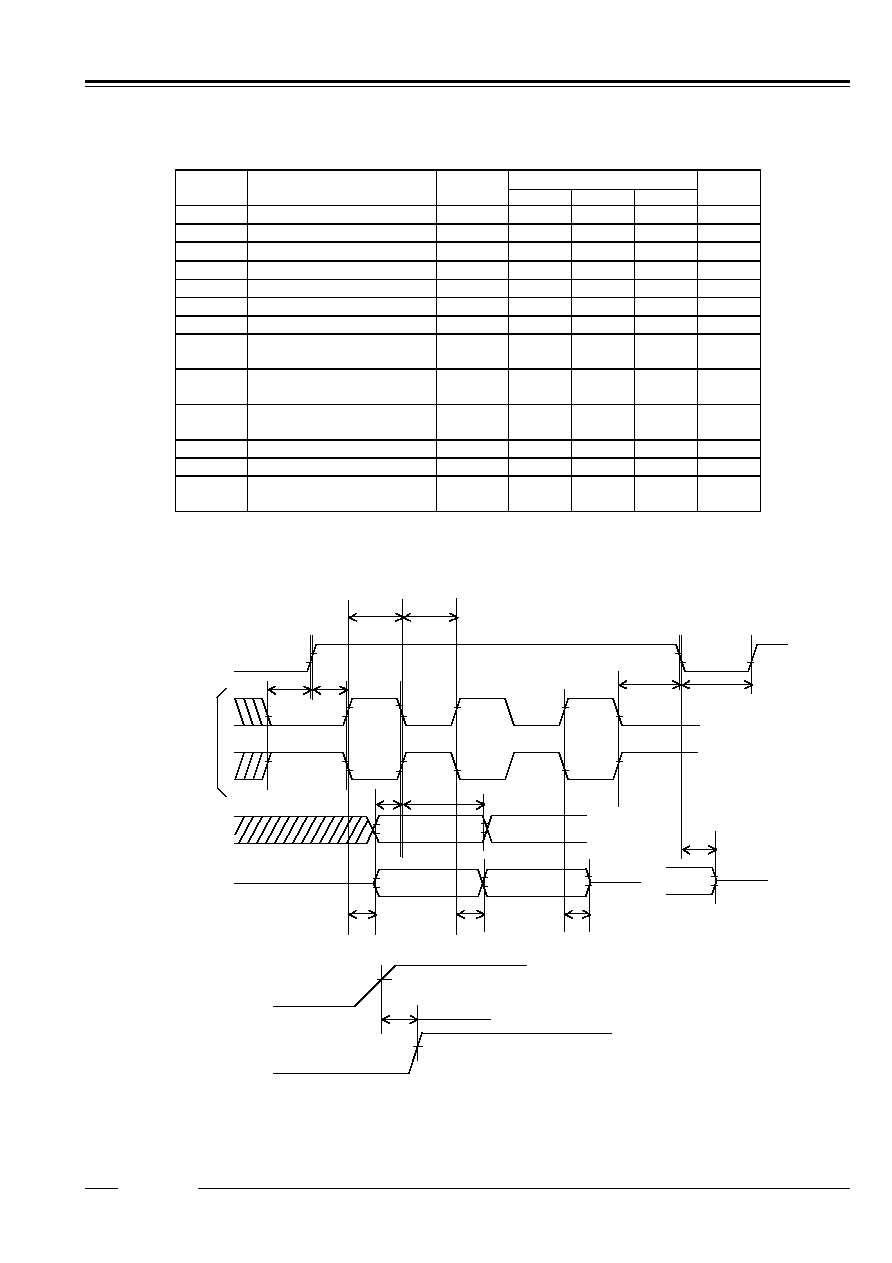
Interfacing with the CPU
q
DATA TRANSFER FORMATS
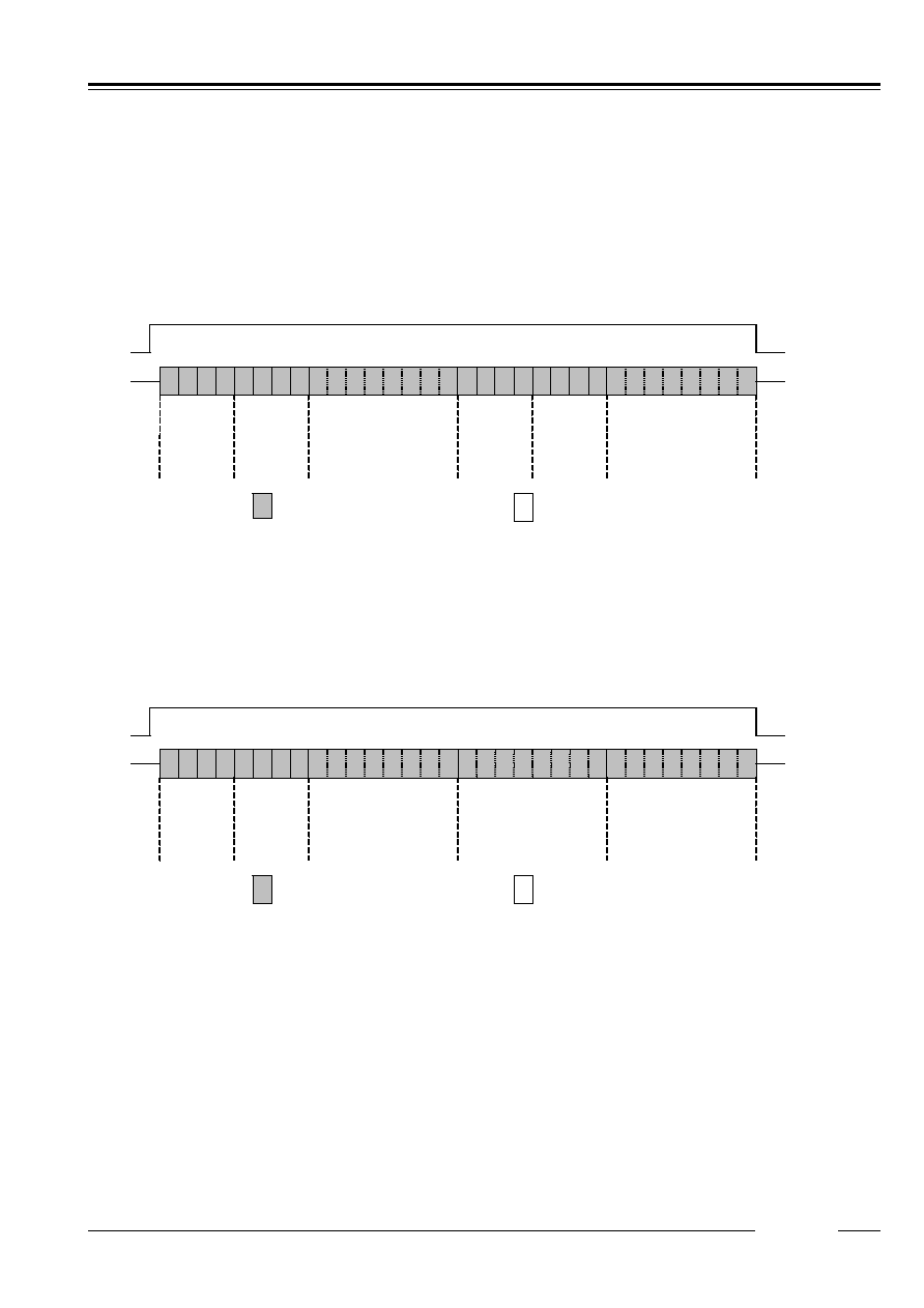
(1) Timing Between CE Pin Transition and Data Input / Output
The R2061 adopts a 3-wire serial interface by which they use the CE (Chip Enable), SCLK (Serial Clock), and
SIO (Serial Input/Output) pins to receive and send data to and from the CPU. The 3-wire serial interface
provides two types of input/output timings with which the SIO pin output and input are synchronized with the rising
or falling edges of the SCLK pin input, respectively, and vice versa. The R2061 is configured to select either one
of two different input/output timings depending on the level of the SCLK pin in the low to high transition of the CE
pin. Namely, when the SCLK pin is held low in the low to high transition of the CE pin, the models will select the
timing with which the SIO pin output is synchronized with the rising edge of the SCLK pin input, and the input is
synchronized with the falling edge of the SCLK pin input, as illustrated in the timing chart below.
SCLK
SIO (for reading)
t
DS
SIO (for writing)
CE
t
CES
t
DH
t
RD
Conversely, when the SCLK pin is held high in the low to high transition of the CE pin, the models will select the
timing with which the SIO pin output is synchronized with the falling edge of the SCLK pin input, and the input is
synchronized with the rising edge of the SCLK pin input, as illustrated in the timing chart below.
SCLK
SIO (for reading)
t
DS
SIO (for writing)
CE
t
CES
t
DH
t
RD
(2) Data Transfer Formats
Data transfer is commenced in the low to high transition of the CE pin input and completed in its high to low
transition. Data transfer is conducted serially in multiple units of 1 byte (8 bits). The former 4 bits are used to
specify in the Address Pointer a head address with which data transfer is to be commenced from the host. The
latter 4 bits are used to select either reading data transfer or writing data transfer, and to set the Transfer Format
Register to specify an appropriate data transfer format. All data transfer formats are designed to transfer the
most significant bit (MSB) first.
A2
CE
SCLK
6
A1
A0
C3
C2
C1
C0
A3
7
5
8
2
3
1
2
3
1
4
D7
D6
D3
D2
D1
D0
Setting
the Address Pointer
Writing or Reading data transfer
Setting the Transfer
Format Register
SIO
Two types of data transfer formats are available for reading data transfer and writing data transfer each.
R2061 Series
12345
Rev.1.03 - 21 -
q
Writing Data Transfer Formats
(1) 1-byte Writing Data Transfer Format
The first type of writing data transfer format is designed to transfer 1-byte data at a time and can be selected by
specifying in the address pointer a head address with which writing data transfer is to be commenced and then
writing the setting of 8h to the transfer format register. This 1-byte writing data transfer can be completed by
driving the CE pin low or continued by specifying a new head address in the address pointer and setting the data
transfer format.
1
1
Data
Data
Example of 1-byte Writing Data Transfer (For Writing Data to Addresses Fh and 7h)
Data transfer from the host
CE
Data transfer from the RTCs
Specifying 7h
in the
Address
Pointer
0
1
0 0
1
1
Setting 8h in
the Transfer
Format
Register
Writing data to
address Fh
Writing data to
address 7h
0
1
1
0 0 0
1 1
Specifying Fh
in the
Address
Pointer
Setting 8h in
the Transfer
Format
Register
SIO
(2) Burst Writing Data Transfer Format
The second type of writing data transfer format is designed to transfer a sequence of data serially and can be
selected by specifying in the address pointer a head address with which writing data transfer is to be commenced
and then writing the setting of 0h to the transfer format register. The address pointer is incremented for each
transfer of 1-byte data and cycled from Fh to 0h. This burst writing data transfer can be completed by driving the
CE pin low.
1
0
Data
Data
Example of Burst Writing Data Transfer (For Writing Data to Addresses Eh, Fh, and 0h)
CE
0
0
0 0
1
1
SIO
Data
Data transfer from the host
Data transfer from the RTCs
Writing data to
address Eh
Specifying Eh
in the
Address
Pointer
Setting 0h in
the Transfer
Format
Register
Writing data to
address Fh
Writing data to
address 0h

R2061 Series
12345
Rev.1.03 - 22 -
q
Reading Data Transfer Formats
(1) 1-byte Reading Data Transfer Format
The first type of reading data transfer format is designed to transfer 1-byte data at a time and can be selected by
specifying in the Address Pointer a head address with which reading data transfer is to be commenced and then
the setting of writing Ch to the Transfer Format Register. This 1-byte reading data transfer can be completed by
driving the CE pin low or continued by specifying a new head address in the Address Pointer and selecting this
type of reading data Transfer Format.
1
0
Data
Data
Example of 1-byte Reading Data Transfer (For Reading Data from Addresses Eh and 2h)
CE
1
1
0 0
1
1
0
1
0
1 0 0
0 1
SIO
Data transfer from the host
Data transfer from the RTCs
Specifying 2h
in the
Address
Pointer
Setting Ch in
the Transfer
Format
Register
Reading data from
address Eh
Reading data from
address 2h
Specifying Eh
in the
Address
Pointer
Setting Ch in
the Transfer
Format
Register
(2) Burst Reading Data Transfer Format
The second type of reading data transfer format is designed to transfer a sequence of data serially and can be
selected by specifying in the address pointer a head address with which reading data transfer is to be
commenced and then writing the setting of 4h to the transfer format register. The address pointer is
incremented for each transfer of 1-byte data and cycled from Fh to 0h. This burst reading data transfer can be
completed by driving the CE pin low.
1
1
DATA
DATA
Example of Burst Reading Data Transfer (For Reading Data from Addresses Fh, 0h, and 1h)
CE
1
0
0 0
1
1
DATA
SIO
Data transfer from the host
Data transfer from the RTCs
Reading data from
address Fh
Specifying Fh
in the
Address
Pointer
Setting 4h in
the Transfer
Format
Register
Reading data from
address 0h
Reading data from
address 1h
R2061 Series
12345
Rev.1.03 - 23 -
(3) Combination of 1-byte Reading and writing Data Transfer Formats
The 1-byte reading and writing data transfer formats can be combined together and further followed by any other
data transfer format.
1
1
DATA
Example of Reading Modify Writing Data Transfer
(For Reading and Writing Data from and to Address Fh)
CE
1
1
0 0
1
1
1
1
1
0 0 0
1 1
DATA
SIO
Data transfer from the host
Data transfer from the RTCs
Writing data to
address Fh
Specifying Fh
in the
Address
Pointer
Setting 8h in
the Transfer
Format
Register
Specifying Fh
in the
Address
Pointer
Setting Ch in
the Transfer
Format
Register
Reading data from
address Fh
The reading and writing data transfer formats correspond to the settings in the transfer format register as shown
in the table below.
1
Byte
Burst
Writing data
transfer
8h
(1,0,0,0)
0h
(0,0,0,0)
Reading data
transfer
Ch
(1,1,0,0)
4h
(0,1,0,0)

R2061 Series
12345
Rev.1.03 - 24 -
q
Considerations in Reading and Writing Time Data under special condition
Any carry to the second digits in the process of reading or writing time data may cause reading or writing
erroneous time data. For example, suppose a carry out of 13:59:59 into 14:00:00 occurs in the process of
reading time data in the middle of shifting from the minute digits to the hour digits. At this moment, the second
digits, the minute digits, and the hour digits read 59 seconds, 59 minutes, and 14 hours, respectively (indicating
14:59:59) to cause the reading of time data deviating from actual time virtually 1 hour. A similar error also occurs
in writing time data. To prevent such errors in reading and writing time data, the R2043 has the function of
temporarily locking any carry to the second digits during the high interval of the CE pin and unlocking such a carry
in its high to low transition. Note that a carry to the second digits can be locked for only 1 second, during which
time the CE pin should be driven low.
CE
Time counts
within RTC
14:00:01
Actual time
13:59:59
Max.62
µ
s
14:00:00
13:59:59 14:00:00 14:00:01
The effective use of this function requires the following considerations in reading and writing time data:
(1) Hold the CE pin high in each session of reading or writing time data.
(2) Ensure that the high interval of the CE pin lasts within 1 second. Should there be any possibility of the host
going down in the process of reading or writing time data, make arrangements in the peripheral circuitry as to
drive the CE pin low or open at the moment that the host actually goes down.
(3) Leave a time span of 31
µ
s or more from the low to high transition of the CE pin to the start of access to
addresses 0h to 6h in order that any ongoing carry of the time digits may be completed within this time span.
(4) Leave a time span of 62
µ
s or more from the high to low transition of the CE pin to its low to high transition in
order that any ongoing carry of the time digits during the high interval of the CE pin may be adjusted within this
time span.
The considerations listed in (1), (3), and (4) above are not required when the process of reading or writing time
data is obviously free from any carry of the time digits.
(e.g. reading or writing time data in synchronization with the periodic interrupt function in the level mode or the
alarm interrupt function).
Good and bad examples of reading and writing time data are illustrated on the next page.

R2061 Series
12345
Rev.1.03 - 25 -
0Ch
Data
Data
Bad Example (1)
(Where the CE pin is once driven low in the process of reading time data)
Less than 62
µ
s
F0h
CE
Time span of less than 31
µ
s
Writing to
Address 0h
(sec.)
0Ch
CE
Bad Example (3)
(Where a time span of less than 62
µ
s is left between the adjacent processes of reading time data)
Good Example
DATA
F4h
DATA
DATA
CE
Address Pointer
= 1h
Transfer Format
Register = 4h
Time span of 31
µ
s or more
Reading from
Address 1h
(min.)
DATA
0Ch Data
Data
31
µ
s or more
Reading from
Address 1h
(min.)
Data
14h
31
µ
s or more
CE
Data transfer from RTCs
0Ch
Data
Data transfer from the host
Bad Example (2)
(Where a time span of less than 31
µ
s is left until the start of the process of writing time data)
Any address other than addresses 0h to 6h
permits of immediate reading or writing without
requiring a time span of 31
µ
s.
SIO
SIO
SIO
SIO
Data
Data
Data
Data
Reading from
Address Fh
(control2)
Reading from
Address 0h
(sec.)
Reading from
Address 2h
(hr.)
Address Pointer
= Fh
Transfer Format
Register = 4h
Address Pointer
= Fh
Transfer Format
Register = 0h
Reading from
Address 0h
(sec.)
Reading from
Address 2h
(hr.)
Address Pointer
= 0h
Transfer Format
Register = Ch
Writing to
Address 1h
(min.)
Writing to
Address 2h
(hr.)
Writing to
Address Fh
(contorl2)
Address Pointer
= 0h
Transfer Format
Register = Ch
Reading from
Address 0h
(sec.)
Reading from
Address 0h
(sec.)
Address Pointer
= 0h
Transfer Format
Register = Ch

R2061 Series
12345
Rev.1.03 - 26 -
s
Configuration of Oscillation Circuit and Correction of Time Count Deviations
q
Configuration of Oscillation Circuit
32kHz
CG
CD
A
OSCIN
OSCOUT
Oscillator
Circuit
The oscillation circuit is driven at a constant voltage of approximately 1.2 volts relative to the level of the VSS pin
input. As such, it is configured to generate an oscillating waveform with a peak-to-peak voltage on the order of
1.1 volts on the positive side of the VSS pin input.
< Considerations in Handling Crystal Oscillators >
Generally, crystal oscillators have basic characteristics including an equivalent series resistance (R1) indicating
the ease of their oscillation and a load capacitance (CL) indicating the degree of their center frequency.
Particularly, crystal oscillators intended for use in the R2061 are recommended to have a typical R1 value of 30k
and a typical CL value of 6 to 8pF. To confirm these recommended values, contact the manufacturers of crystal
oscillators intended for use in these particular models.
< Considerations in Installing Components around the Oscillation Circuit >
1)
Install the crystal oscillator in the closest possible vicinity to the real-time clock ICs.
2)
Avoid laying any signal lines or power lines in the vicinity of the oscillation circuit (particularly in the area
marked "A" in the above figure).
3)
Apply the highest possible insulation resistance between the OSCIN and OSCOUT pins and the printed
circuit board.
4)
Avoid using any long parallel lines to wire the OSCIN and OSCOUT pins.
5)
Take extreme care not to cause condensation, which leads to various problems such as oscillation halt.
< Other Relevant Considerations >
1)
For external input of 32.768-kHz clock pulses to the OSCIN pin:
DC coupling: Prohibited due to an input level mismatch.
AC coupling: Permissible except that the oscillation halt sensing circuit does not guarantee perfect
operation because it may cause sensing errors due to such factors as noise.
2)
To maintain stable characteristics of the crystal oscillator, avoid driving any other IC through 32.768-kHz
clock pulses output from the OSCOUT pin.
Typical externally-equipped element
X'tal
:
32.768kHz
(R1=30k
typ)
(CL=6pF
to
8pF)
Standard values of internal elements
CG,CD 10pF typ

R2061 Series
12345
Rev.1.03 - 27 -
q
Measurement of Oscillation Frequency
Frequency
Counter
32768Hz
VCC
OSCIN
OSCOUT
VDD
/INTR
VSS
* 1) The R2061 is configured to generate 1Hz clock pulses for output from the /INTR pin by setting
(00XX0011) at address Eh.
* 2) A frequency counter with 6 (more preferably 7) or more digits on the order of 1ppm is recommended
for use in the measurement of the oscillation frequency of the oscillation circuit.
q
Adjustment of Oscillation frequency
The oscillation frequency of the oscillation circuit can be adjusted by varying procedures depending on the usage
of Model R2061 in the system into which they are to be built and on the allowable degree of time count errors.
Course (A)
When the time count precision of each RTC is not to be adjusted, the crystal oscillator intended for use in that
RTC may have any CL value requiring no presetting. The crystal oscillator may be subject to frequency
variations which are selectable within the allowable range of time count precision. Several crystal oscillators and
RTCs should be used to find the center frequency of the crystal oscillators by the method described in "P27
q
Measurement of Oscillation Frequency" and then calculate an appropriate oscillation adjustment value by the
method described in "P29
q
Oscillation Adjustment Circuit" for writing this value to the R2061.
Course (B)
When the time count precision of each RTC is to be adjusted within the oscillation frequency variations of the
crystal oscillator plus the frequency variations of the real-time clock ICs, it becomes necessary to correct
deviations in the time count of each RTC by the method described in " P29
q
Oscillation Adjustment Circuit".
Such oscillation adjustment provides crystal oscillators with a wider range of allowable settings of their oscillation
frequency variations and their CL values. The real-time clock IC and the crystal oscillator intended for use in that
real-time clock IC should be used to find the center frequency of the crystal oscillator by the method described in "
P27
q
Measurement of Oscillation Frequency" and then confirm the center frequency thus found to fall within
the range adjustable by the oscillation adjustment circuit before adjusting the oscillation frequency of the
oscillation circuit. At normal temperature, the oscillation frequency of the oscillator circuit can be adjusted by up
to approximately
±
0.5ppm.
* 1) Generally, crystal oscillators for commercial use are classified in terms of their center frequency
depending on their load capacitance (CL) and further divided into ranks on the order of
±
10,
±
20, and
±
50ppm depending on the degree of their oscillation frequency variations.
* 2) Basically, Model R2061 is configured to cause frequency variations on the order of
±
5 to
±
10ppm at
25
∞
C.
* 3) Time count precision as referred to in the above flow chart is applicable to normal temperature and
actually affected by the temperature characteristics and other properties of crystal oscillators.
R2061 Series
12345
Rev.1.03 - 28 -
The R2061, which incorporate the CG and the CD, require adjusting the oscillation frequency of the crystal
oscillator through its CL value.
Generally, the relationship between the CL value and the CG and CD values can be represented by the
following equation:
CL = (CG
◊
CD)/(CG + CD) + CS where "CS" represents the floating capacity of the printed circuit board.
The crystal oscillator intended for use in the R2061 is recommended to have the CL value on the order of 6
to 8pF. Its oscillation frequency should be measured by the method described in " P27
q
Measurement of
Oscillation Frequency". Any crystal oscillator found to have an excessively high or low oscillation frequency
(causing a time count gain or loss, respectively) should be replaced with another one having a smaller and
greater CL value, respectively until another one having an optimum CL value is selected. In this case, the
bit settings disabling the oscillation adjustment circuit (see " P29
q
Oscillation Adjustment Circuit ") should
be written to the oscillation adjustment register.
Incidentally, the high oscillation frequency of the crystal oscillator can also be adjusted by adding an external
oscillation stabilization capacitor CGOUT as illustrated in the diagram below.
32kHz
RD
CG
CD
OSCIN
OSCOUT
CGOUT
*1)
Oscillator
Circuit
*1) The CGOUT should have a capacitance ranging
from 0 to 15 pF.

R2061 Series
12345
Rev.1.03 - 29 -
q
Oscillation Adjustment Circuit
The oscillation adjustment circuit can be used to correct a time count gain or loss with high precision by varying
the number of 1-second clock pulses once per 20 seconds or 60 seconds. When DEV bit in the Oscillation
Adjustment Register is set to 0, R2061 varies number of 1-second clock pulses once per 20 seconds. When
DEV bit is set to 1, R2061 varies number of 1-second clock pulses once per 60 seconds. The oscillation
adjustment circuit can be disabled by writing the settings of "*, 0, 0, 0, 0, 0, *" ("*" representing "0" or "1") to the F6,
F5, F4, F3, F2, F1, and F0 bits in the oscillation adjustment circuit. Conversely, when such oscillation
adjustment is to be made, an appropriate oscillation adjustment value can be calculated by the equation below for
writing to the oscillation adjustment circuit.
(1) When Oscillation Frequency (* 1) Is Higher Than Target Frequency (* 2) (Causing Time Count Gain)
When DEV=0:
Oscillation adjustment value (*3) = (Oscillation frequency - Target Frequency + 0.1)
Oscillation frequency
◊
3.051
◊
10
-6
(Oscillation Frequency ≠ Target Frequency)
◊
10 + 1
When DEV=1:
Oscillation adjustment value (*3) = (Oscillation frequency - Target Frequency + 0.0333)
Oscillation frequency
◊
1.017
◊
10
-6
(Oscillation Frequency ≠ Target Frequency)
◊
30 + 1
* 1)
Oscillation frequency:
32768 times the frequency of 1Hz clock pulse output from the /INTR pin at normal temperature in the
manner described in " P27
q
Measurement of Oscillation Frequency".
* 2)
Target frequency:
Desired frequency to be set. Generally, a 32.768-kHz crystal oscillator has such temperature
characteristics as to have the highest oscillation frequency at normal temperature. Consequently, the
crystal oscillator is recommended to have target frequency settings on the order of 32.768 to 32.76810
kHz (+3.05ppm relative to 32.768 kHz). Note that the target frequency differs depending on the
environment or location where the equipment incorporating the RTC is expected to be operated.
* 3)
Oscillation adjustment value:
Value that is to be finally written to the F0 to F6 bits in the Oscillation Adjustment Register and is
represented in 7-bit coded decimal notation.
(2) When Oscillation Frequency Is Equal To Target Frequency (Causing Time Count neither Gain nor Loss)
Oscillation adjustment value = 0, +1, -64, or ≠63
(3) When Oscillation Frequency Is Lower Than Target Frequency (Causing Time Count Loss)
When DEV=0:
Oscillation adjustment value = (Oscillation frequency - Target Frequency)
Oscillation frequency
◊
3.051
◊
10
-6
(Oscillation Frequency ≠ Target Frequency)
◊
10
When DEV=1:
Oscillation adjustment value = (Oscillation frequency - Target Frequency)
Oscillation frequency
◊
1.017
◊
10
-6
(Oscillation Frequency ≠ Target Frequency)
◊
30
Oscillation adjustment value calculations are exemplified below
(A) For an oscillation frequency = 32768.85Hz and a target frequency = 32768.05Hz
When setting DEV bit to 0:
Oscillation adjustment value = (32768.85 - 32768.05 + 0.1) / (32768.85
◊
3.051
◊
10
-6
)
(32768.85 - 32768.05)
◊
10 + 1
= 9.001
9
In this instance, write the settings (DEV,F6,F5,F4,F3,F2,F1,F0)=(0,0,0,0,1,0,0,1) in the oscillation adjustment
register. Thus, an appropriate oscillation adjustment value in the presence of any time count gain represents a
distance from 01h.
When setting DEV bit to 1:

R2061 Series
12345
Rev.1.03 - 30 -
Oscillation adjustment value = (32768.85 - 32768.05 + 0.0333) / (32768.85
◊
1.017
◊
10
-6
)
(32768.85 - 32768.05)
◊
30 + 1
= 23.51
24
In this instance, write the settings (DEV,F6,F5,F4,F3,F2,F1,F0)=(1,0,0,1,1,0,0,0) in the oscillation adjustment
register.
(B) For an oscillation frequency = 32762.22Hz and a target frequency = 32768.05Hz
When setting DEV bit to 0:
Oscillation adjustment value = (32762.22 - 32768.05) / (32762.22
◊
3.051
◊
10
-6
)
(32762.22 - 32768.05)
◊
10
= -58.325
-58
To represent an oscillation adjustment value of - 58 in 7-bit coded decimal notation, subtract 58 (3Ah) from 128
(80h) to obtain 46h. In this instance, write the settings of (DEV,F6,F5,F4,F3,F2,F1,F0) = (0,1,0,0,0,1,1,0) in the
oscillation adjustment register. Thus, an appropriate oscillation adjustment value in the presence of any time
count loss represents a distance from 80h.
When setting DEV bit to 1:
Oscillation adjustment value = (32762.22 - 32768.05) / (32762.22
◊
1.017
◊
10
-6
)
(32762.22 - 32768.05)
◊
30
= -174.97
-175
Oscillation adjustment value can be set from -62 to 63. Then, in this case, Oscillation adjustment value is out of
range.
(4) Difference between DEV=0 and DEV=1
Difference between DEV=0 and DEV=1 is following,
DEV=0 DEV=1
Maximum value range
-189.2ppm to 189.2ppm
-62ppm to 63ppm
Minimum resolution
3ppm
1ppm
Notes:
If following 3 conditions are completed, actual clock adjustment value could be different from target
adjustment value that set by oscillator adjustment function.
1. Using oscillator adjustment function
2. Access to R2051 at random, or synchronized with external clock that has no relation to R2051, or
synchronized with periodic interrupt in pulse mode.
3. Access to R2051 more than 2 times per each second on average.
For more details, please contact to Ricoh.
q
How to evaluate the clock gain or loss
The oscillator adjustment circuit is configured to change time counts of 1 second on the basis of the settings of
the oscillation adjustment register once in 20 seconds or 60 seconds. The way to measure the clock error as
follows:
(1) Output a 1Hz clock pulse of Pulse Mode with interrupt pin
Set (0,0,x,x,0,0,1,1) to Control Register 1 at address Eh.
(2) After setting the oscillation adjustment register, 1Hz clock period changes every 20seconds ( or every 60
seconds) like next page figure.

R2061 Series
12345
Rev.1.03 - 31 -
1Hz clock pulse
T0
T0
T0
T1
1 time
19 times
Measure the interval of T0 and T1 with frequency counter. A frequency counter with 7 or more digits is
recommended for the measurement.
(3) Calculate the typical period from T0 and T1
T = (19
◊
T0+1
◊
T1)/20
Calculate the time error from T.
R2061 Series
12345
Rev.1.03 - 32 -
s
Power-on Reset, Oscillation Halt Sensing, and Supply Voltage Monitoring
q
PON, /XST, and VDET
The power-on reset circuit is configured to reset control register1, 2, and clock adjustment register when VDD
power up from 0v. The oscillation halt sensing circuit is configured to record a halt on oscillation by 32.768-kHz
clock pulses. The supply voltage monitoring circuit is configured to record a drop in supply voltage below a
threshold voltage of 2.1 or 1.35v.
Each function has a monitor bit. I.e. the PON bit is for the power-on reset circuit, and /XST bit is for the
oscillation halt sensing circuit, and VDET is for the supply voltage monitoring circuit. PON and VDET bits are
activated to "H". However, /XST bit is activated to "L". The PON and VDET accept only the writing of 0, but /XST
accepts the writing of 0 and 1. The PON bit is set to 1, when VDD power-up from 0V, but VDET is set to 0, and
/XST is
indefinite.
The functions of these three monitor bits are shown in the table below.
PON
/XST
VDET
Function Monitoring
for
the
power-on reset function
Monitoring for the
oscillation halt sensing
function
a drop in supply voltage
below a threshold voltage
of 2.1 or 1.35v
Address
D4 in Address Fh
D5 in Address Fh
D6 in Address Fh
Activated High
Low
High
When VDD power
up from 0v
1 indefinite
0
accept the writing
0 only
Both 0 and 1
0 only
The relationship between the PON, /XST, and VDET is shown in the table below.
PON
/XST VDET
Conditions of supply voltage and
oscillation
Condition of oscillator, and back-up
status
0
0
0
Halt on oscillation, but no drop in
VDD supply voltage below threshold
voltage
Halt on oscillation cause of
condensation etc.
0
0
1
Halt on oscillation and drop in VDD
supply voltage below threshold
voltage, but no drop to 0V
Halt on oscillation cause of drop in
back-up battery voltage
0
1
0
No drop in VDD supply voltage below
threshold voltage and no halt in
oscillation
Normal condition
0
1
1
Drop in VDD supply voltage below
threshold voltage and no halt on
oscillation
No halt on oscillation, but drop in
back-up battery voltage
1
*
*
Drop in supply voltage to 0v
Power-up from 0v,
32768Hz Oscillation
Power-on reset flag
(PON)
Oscillation halt
sensing flag (/XST)
Threshold voltage (2.1V or 1.35V)
VDD
VDD supply voltage
monitor flag (VDET)
Internal initialization
period (1 to 2 sec.)
VDET
0
/XST
1
PON
0
VDET
0
/XST
1
PON
1
VDET
0
/XST
1
PON
0
Internal initialization
period (1 to 2 sec.)
When the PON bit is set to 1 in the control register 2, the DEV, F6 to F0, WALE, DALE, /12
24, SCRATCH2,

R2061 Series
12345
Rev.1.03 - 33 -
TEST, CT2, CT1, CT0, VDSL, VDET, SCRATCH1, CTFG, WAFG, and DAFG bits are reset to 0 in the oscillation
adjustment register, the control register 1, and the control register 2. The PON bit is also set to 1 at power-on
from 0 volts.
< Considerations in Using Oscillation Halt Sensing Circuit >
Be sure to prevent the oscillation halt sensing circuit from malfunctioning by preventing the following:
1) Instantaneous power-down on the VDD
2) Condensation on the crystal oscillator
3) On-board noise to the crystal oscillator
4) Applying to individual pins voltage exceeding their respective maximum ratings
In particular, note that the /XST bit may fail to be set to 0 in the presence of any applied supply voltage as
illustrated below in such events as backup battery installation. Further, give special considerations to prevent
excessive chattering in the oscillation halt sensing circuit.
VDD

R2061 Series
12345
Rev.1.03 - 34 -
q
Voltage Monitoring Circuit
R2061 incorporates two kinds of voltage monitoring function. These are shown in the table below.
VCC Voltage Monitoring Circuit
VCC Voltage Monitoring Circuit
(VDET)
Purpose
CPU reset output
Back-up battery checker
Monitoring supply voltage
VCC pin
VDD pin (supply voltage for the
internal RTC circuit)
Output for result
/VDCC pin
Store in the Control Register 2
(D6 in Address Fh)
Function
After falling VCC, /VDCC outputs
"L". tDEALY after rising VCC,
/VDCC outputs "H" (OFF)
Below the threshold voltage, SW1
turns off and SW2 turns on. Over
the threshold voltage, SW1 turns
on and SW2 turns off.
Detector Threshold (falling edge
of power supply voltage)
-VDET1
Selecting from VDETH or VDETL
by writing to the register
(D7 in Address Fh)
Detector Released
Voltage (rising edge of power
supply voltage)
+VDET1
Same as falling edge
( No hysteresis)
The way to monitor
Always
One time every second
The VDD supply voltage monitoring circuit is configured to conduct a sampling operation during an interval of
7.8ms per second to check for a drop in supply voltage below a threshold voltage of 2.1 or 1.35v for the VDSL bit
setting of 0 (the default setting) or 1, respectively, in the Control Register 2, thus minimizing supply current
requirements as illustrated in the timing chart below. This circuit suspends a sampling operation once the VDET
bit is set to 1 in the Control Register 2. The VDD supply voltage monitor is useful for back-up battery checking.
VDET
(D6 in Address Fh)
PON
VDD
2.1v or 1.35v
1s
VDET
0
7.8ms
Sampling timing for VDD
supply voltage monitor
Internal nitiali-
zation period
(1 to 2sec.)
PON
0
VDET
0
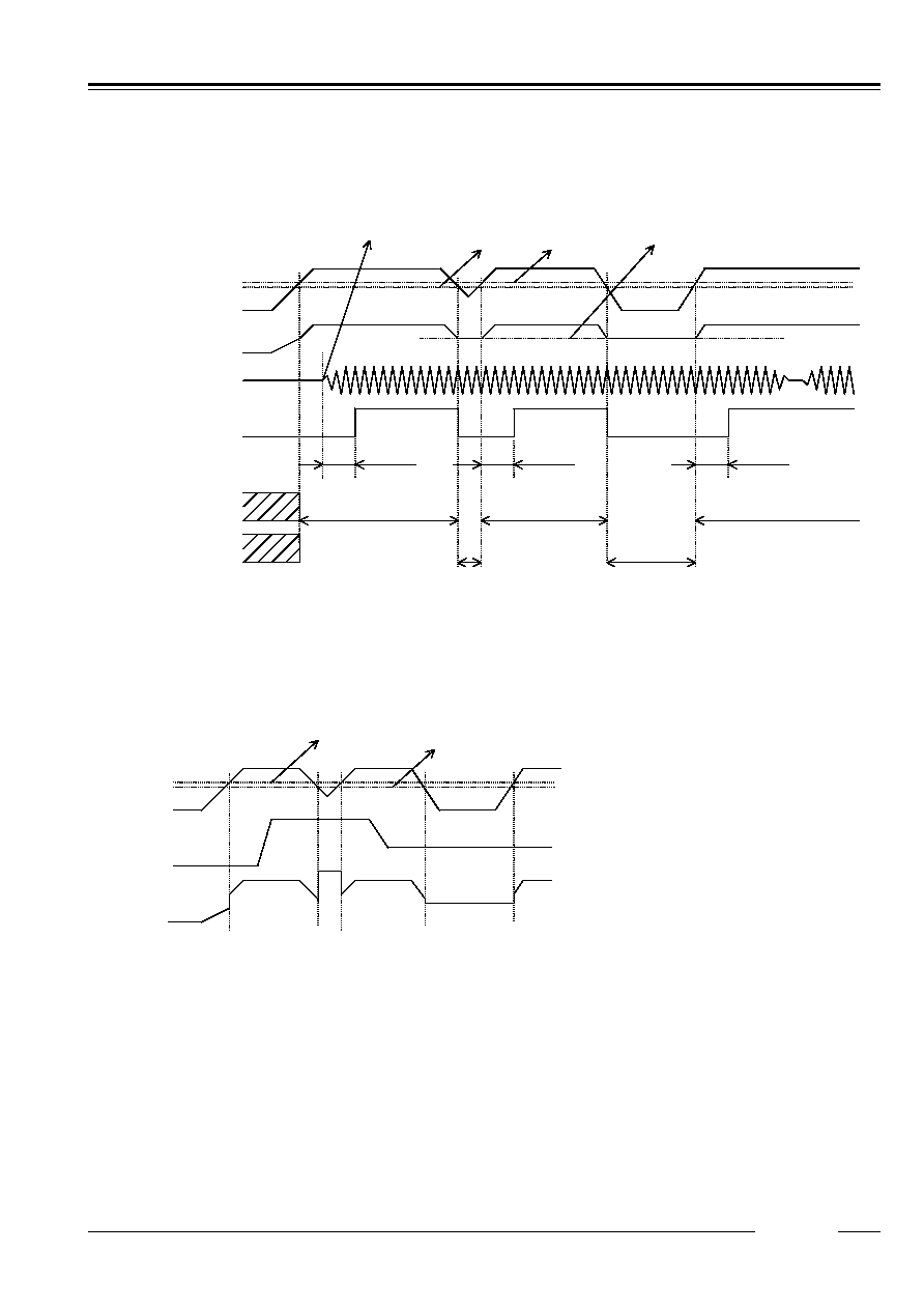
R2061 Series
12345
Rev.1.03 - 35 -
The VCC supply voltage monitor circuit operates always. When VCC rising over +VDET1, SW1 turns on, and
SW2 turns off. And tDELAY after rising VCC, /VDCC outputs OFF(H). But when oscillation is halt, VCC outputs
OFF(H) tDELAY after oscillation starting. When VCC falling beyond -VDET1, SW1 turns off, and SW2 turns on.
And /VDCC outputs "L".
VDD
32768Hz Oscillation
/VDCC
+VDET1
VCC
SW1
SW2
tDELAY
tDELAY
tDELAY
ON
ON
ON
ON
ON
Same voltage level as VSB
Oscillation starting
-VDET1
s
Battery Switch Over Circuit
R2061 incorporates three power supply pins, VDD, VCC, and VSB. VDD pin is the power supply pin for internal
real time clock circuit. When VCC voltage is lower than
±
VDET, VSB supplies the power to VDD, and when
higher than
±
VDET, VCC supplies the power to VDD. The timing chart for VCC, VDD, and VSB is shown
following.
VDD
+VDET1
VCC
VSB
(1)
(2)
(3)
(3)
(2)
-VDET1
(1) When VSB is 0v and VCC is rising from 0v, VDD follows half of VCC voltage level. After VCC rising over
+VDET, VDD follows VCC voltage level.
(2) When VCC is higher than +VDET, VDD level is equal to VCC.
(3) After VCC falling beyond -VDET, VDD level is equal to VSB.

R2061 Series
12345
Rev.1.03 - 36 -
s
Alarm and Periodic Interrupt
The R2061 incorporates the alarm interrupt circuit and the periodic interrupt circuit that are configured to generate
alarm signals and periodic interrupt signals for output from the /INTR pin as described below.
(1) Alarm Interrupt Circuit
The alarm interrupt circuit is configured to generate alarm signals for output from the /INTR, which is driven low
(enabled) upon the occurrence of a match between current time read by the time counters (the day-of-week, hour,
and minute counters) and alarm time preset by the alarm registers (the Alarm_W registers intended for the
day-of-week, hour, and minute digit settings and the Alarm_D registers intended for the hour and minute digit
settings).
(2) Periodic Interrupt Circuit
The periodic interrupt circuit is configured to generate either clock pulses in the pulse mode or interrupt signals in
the level mode for output from the /INTR pin depending on the CT2, CT1, and CT0 bit settings in the control
register 1.
The above two types of interrupt signals are monitored by the flag bits (i.e. the WAFG, DAFG, and CTFG bits in
the Control Register 2) and enabled or disabled by the enable bits (i.e. the WALE, DALE, CT2, CT1, and CT0 bits
in the Control Register 1) as listed in the table below.
Flag bits
Enable bits
Alarm_W WAFG
(D1 at Address Fh)
WALE
(D7 at Address Eh)
Alarm_D DAFG
(D0 at Address Fh)
DALE
(D6 at Address Eh)
Peridic interrupt
CTFG
(D2 at Address Fh)
CT2=CT1=CT0=0
(These bit setting of "0" disable the Periodic Interrupt)
(D2 to D0 at Address Eh)
* At power-on, when the WALE, DALE, CT2, CT1, and CT0 bits are set to 0 in the Control Register 1,
the /INTR pin is driven high (disabled).
* When two types of interrupt signals are output simultaneously from the /INTR pin, the output from the
/INTR pin becomes an OR waveform of their negative logic.
Example: Combined Output to /INTR Pin Under Control of
/ALARM_D and Periodic Interrupt
Periodic Interrupt
/INTR
/Alarm_D
In this event, which type of interrupt signal is output from the /INTR pin can be confirmed by reading the
DAFG,
and CTFG bit settings in the Control Register 2.
q
Alarm Interrupt
The alarm interrupt circuit is controlled by the enable bits (i.e. the WALE and DALE bits in the Control Register 1)
and the flag bits (i.e. the WAFG and DAFG bits in the Control Register 2). The enable bits can be used to
enable this circuit when set to 1 and to disable it when set to 0. When intended for reading, the flag bits can be
used to monitor alarm interrupt signals. When intended for writing, the flag bits will cause no event when set to 1
and will drive high (disable) the alarm interrupt circuit when set to 0.
The enable bits will not be affected even when the flag bits are set to 0. In this event, therefore, the alarm
interrupt circuit will continue to function until it is driven low (enabled) upon the next occurrence of a match
between current time and preset alarm time.

R2061 Series
12345
Rev.1.03 - 37 -
The alarm function can be set by presetting desired alarm time in the alarm registers (the Alarm_W Registers for
the day-of-week digit settings and both the Alarm_W Registers and the Alarm_D Registers for the hour and
minute digit settings) with the WALE and DALE bits once set to 0 and then to 1 in the Control Register 1. Note
that the WALE and DALE bits should be once set to 0 in order to disable the alarm interrupt circuit upon the
coincidental occurrence of a match between current time and preset alarm time in the process of setting the
alarm function.
current time =
preset alarm time
WALE
1
(DALE)
Interval (1min.) during which a match
between current time and preset alarm time
occurs
current time =
preset alarm time
WAFG
0
(DAFG)
/INTR
WALE
1
(DALE)
WALE
1
(DALE)
current time =
preset alarm time
WALE
0
(DALE)
current time =
preset alarm time
/INTR
After setting WALE(DALW) to 0, Alarm registers is set to current time, and WALE(DALE) is set to 1, /INTR will be
not driven to "L" immediately, /INTR will be driven to "L" at next alarm setting time.
q
Periodic Interrupt
Setting of the periodic selection bits (CT2 to CT0) enables periodic interrupt to the CPU. There are two waveform
modes: pulse mode and level mode. In the pulse mode, the output has a waveform duty cycle of around 50%. In
the level mode, the output is cyclically driven low and, when the CTFG bit is set to 0, the output is return to High
(OFF).
Description
CT2 CT1 CT0
Wave form mode
Interrupt Cycle and Falling Timing
0 0 0 -
OFF(H)
(Default)
0 0 1 -
Fixed
at
"L"
0 1 0 Pulse
Mode
*1) 2Hz(Duty50%)
0 1 1 Pulse
Mode
*1) 1Hz(Duty50%)
1
0
0
Level Mode *2)
Once per 1 second (Synchronized with
Second counter increment)
1
0
1
Level Mode *2)
Once per 1 minute (at 00 seconds of every
Minute)
1
1
0
Level Mode *2)
Once per hour (at 00 minutes and 00
Seconds of every hour)
1
1
1
Level Mode *2)
Once per month (at 00 hours, 00 minutes,
and 00 seconds of first day of every month)
*1) Pulse Mode:
2-Hz and 1-Hz clock pulses are output in synchronization with the increment of the second counter as
illustrated in the timing chart below.
/INTR Pin
Rewriting of the second counter
CTFG Bit
Approx. 92
µ
s
(Increment of second counter)

R2061 Series
12345
Rev.1.03 - 38 -
In the pulse mode, the increment of the second counter is delayed by approximately 92
µ
s from the
falling edge of clock pulses. Consequently, time readings immediately after the falling edge of clock
pulses may appear to lag behind the time counts of the real-time clocks by approximately 1 second.
Rewriting the second counter will reset the other time counters of less than 1 second, driving the
/INTR pin low.
*2) Level Mode:
Periodic interrupt signals are output with selectable interrupt cycle settings of 1 second, 1 minute, 1
hour, and 1 month. The increment of the second counter is synchronized with the falling edge of
periodic interrupt signals. For example, periodic interrupt signals with an interrupt cycle setting of 1
second are output in synchronization with the increment of the second counter as illustrated in the
timing chart below.
/INTR Pin
(Increment of
second counter)
CTFG Bit
Setting CTFG bit to 0
Setting CTFG bit to 0
(Increment of
second counter)
(Increment of
second counter)
*1), *2) When the oscillation adjustment circuit is used, the interrupt cycle will fluctuate once per 20sec. as
follows:
Pulse Mode: The "L" period of output pulses will increment or decrement by a maximum of
±
3.784ms. For
example, 1-Hz clock pulses will have a duty cycle of 50
±
0.3784%.
Level Mode: A periodic interrupt cycle of 1 second will increment or decrement by a maximum of
±
3.784 ms.

R2061 Series
12345
Rev.1.03 - 39 -
s
Typical Applications
q
Typical Power Circuit Configurations
VDD
VSB
VCC
VSS
0.1
µ
F
CPU Power
Supply
The case of back-up by
primary battery
CR2025
etc.
VSB
VDD
VCC
VSS
0.1
µ
F
CPU power
supply
ML614
etc.
The case of back-up by
capacitor or secondary battery
(Charging voltage is equal to CPU
power supply voltage)
VSB
VDD
VCC
VSS
0.1
µ
F
CPU power
supply
(3V)
5V
Double layer
capacitor
etc.
The case of back-up by
capacitor or secondary battery
(Charging voltage is not equal to
CPU power supply voltage)
VDD pin cannot be connect to any additional heavy load components such as SRAM. And VDD pin must be
connected C2, and C2 should be over 0.1
µ
F.
VDD
CPU power supply
VCC
VSB
C3
VOLTAGE
DETECTOR
SW1
SW2
C2
R1
CPU
Vbat
-VDET1
Rcpu
R2061 Series
When secondary battery or double layer capacitor connects to VDD pin, after CPU power supply turning off,
secondray battery discharges through the root above figure. If R1 is much smaller than CPU impedance (Rcpu),
VCC voltage keeps higher than -VDET1, and SW1 keeps on. Therefore R1 must be specified by following
formula.
R1 > Rcpu x (Vbat - (-VDET1)) / (-VDET1)
R1 is specified by back-up battery or double layer capacitor, too. Please check the data sheet for back-up
devices.
q
Connection of CIN pin
Please connect capacitor over 0.1
µ
F between CIN and VSS pin.
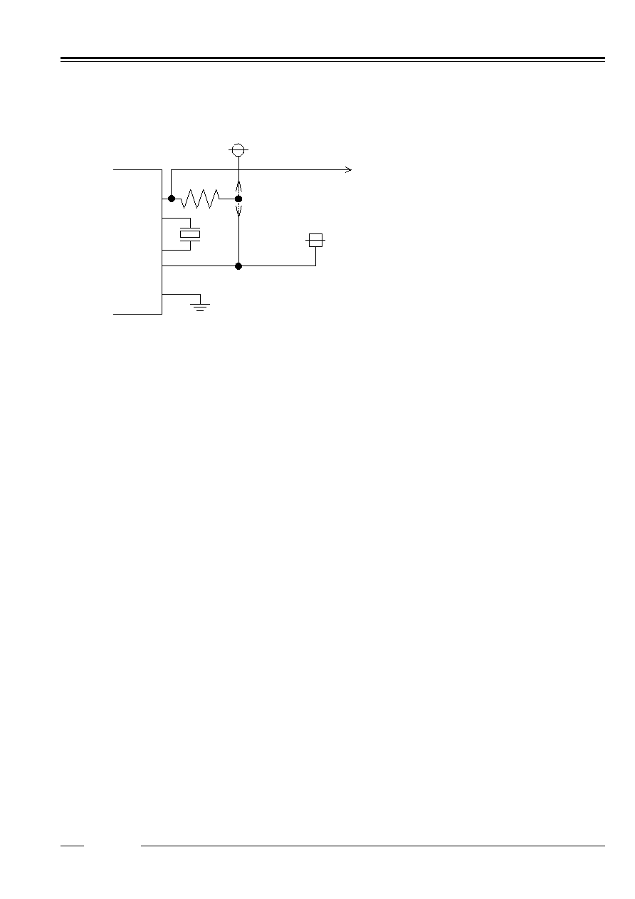
R2061 Series
12345
Rev.1.03 - 40 -
q
Connection of /INTR and /VDCC Pin
The /INTR and /VDCC pins follow the N-channel open drain output logic and contains no protective diode on the
power supply side. As such, it can be connected to a pull-up resistor of up to 5.5 volts regardless of supply
voltage.
VSB
OSCIN
OSCOUT
/INTR or /VDCC
*1)
32768Hz
B
A
Backup power supply
CPU power supply
VSS
*1) Depending on whether the /INTR and /VDCC
pins are to be used during battery backup, it
should be connected to a pull-up resistor at
the following different positions:
(1) Position A in the left diagram when it is not to
be used during battery backup.
(2) Position B in the left diagram when it is to be
used during battery backup.
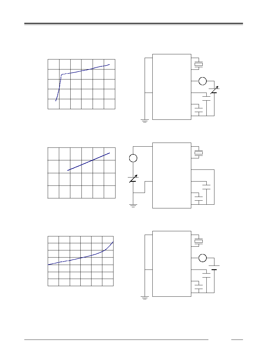
R2061 Series
12345
Rev.1.03 - 41 -
s
Typical Characteristics
q
Time keeping current (ISB) vs. Supply voltage (VSB)
(Topt=25
∞
C) Test Circuit
0
0.1
0.2
0.3
0.4
0.5
0
1
2
3
4
5
6
VSB(v)
Time keeping current (uA
)
VCC
VSB
VDD
CIN
VSS
OSCIN
OSCOUT
/INTR
/VDCC
CE
SCLK
SIO
0.1
µ
F
0.1
µ
F
A
q
Stand-by current (ICC) vs. Supply voltage (VCC)
(Topt=25
∞
C) Test circuit
0
0.5
1
1.5
2
0
1
2
3
4
5
6
VCC(v)
S
t
and-by Current
(uA
)
VCC
VSB
VDD
CIN
VSS
OSCIN
OSCOUT
/INTR
/VDCC
CE
SCLK
SIO
0.1
µ
F
0.1
µ
F
A
q
Time keeping current (ISB) vs. Operating Temperature (Topt)
(VSB=3V) Test circuit
0
0.1
0.2
0.3
0.4
0.5
0.6
0.7
-50
-25
0
25
50
75
100
Operating Temperature (Celsius)
Time keeping current (uA
)
VCC
VSB
VDD
CIN
VSS
OSCIN
OSCOUT
/INTR
/VDCC
CE
SCLK
SIO
0.1
µ
F
0.1
µ
F
A

R2061 Series
12345
Rev.1.03 - 42 -
q
Stand-by current (ICC) vs. Operating Temperature (Topt)
(VCC=3V) Test circuit
0
0.5
1
1.5
2
-50
-25
0
25
50
75
100
Operating temperature (Celsius)
S
t
and-by current
(uA
)
VCC
VSB
VDD
CIN
VSS
OSCIN
OSCOUT
/INTR
/VDCC
CE
SCLK
SIO
0.1
µ
F
0.1
µ
F
A
q
CPU access current vs. SCLK clock frequency (kHz)
(Topt=25
∞
C)
0
20
40
60
80
0
200
400
600
800
1000
SCL clock frequency (KHz)
CPU access cur
r
ent
(
u
A)
q
Oscillation frequency deviation (
f/f0) vs. Operating temperature (Topt)
(VCC=3V Topt=25
∞
C as standard) Test circuit
-160
-140
-120
-100
-80
-60
-40
-20
0
20
-50 -25
0
25
50
75 100
Operating temperature Topt(Celsius)
O
scillation fr
equency deviation
df/f0(ppm)
VCC
VSB
VDD
CIN
VSS
OSCIN
OSCOUT
/INTR
/VDCC
CE
SCLK
SIO
0.1
µ
F
0.1
µ
F
Frequency
counter
VCC=5v
VCC=3v
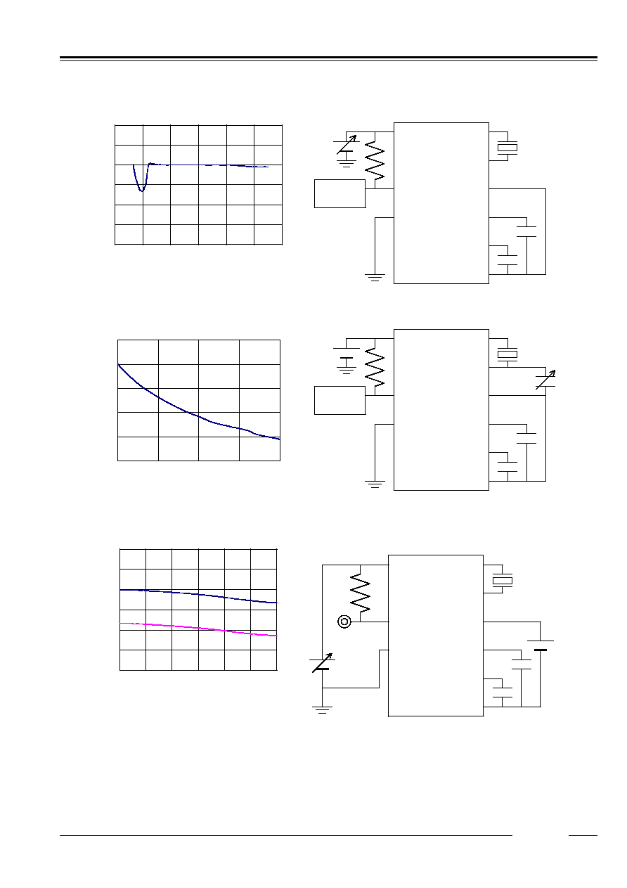
R2061 Series
12345
Rev.1.03 - 43 -
q
Frequency deviation (
f/f0) vs. Supply voltage (VSB/VCC)
(Topt=25
∞
C) VCC/VSB=3V as standard Test circuit
-4
-3
-2
-1
0
1
2
0
1
2
3
4
5
6
VCC/VSB(v)
Frequenc
y
dev
iation d
f/f0(ppm)
VCC
VSB
VDD
CIN
VSS
OSCIN
OSCOUT
/INTR
/VDCC
CE
SCLK
SIO
0.1
µ
F
0.1
µ
F
Frequency
counter
q
Frequency deviation (
f/f0) vs. CGOUT
(Topt=25
∞
C, VCC=3V)CGOUT=0pF as standard Test circuit
-40
-30
-20
-10
0
10
0
5
10
15
20
CGOUT(pF)
F
r
equency devi
a
t
i
on d
f/f0
(p
p
m
)
VCC
VSB
VDD
CIN
VSS
OSCIN
OSCOUT
/INTR
/VDCC
CE
SCLK
SIO
0.1
µ
F
0.1
µ
F
Frequency
counter
q
Detector threshold voltage (+VDET1/-VDET1) vs. Operating temperature (Topt) (R2061K01)
(VSB=3V) Test circuit
1.6
1.7
1.8
1.9
-50
-25
0
25
50
75
100
Operating Temperature Topt(Celsius)
D
e
tector threshold voltage
±VDET1
(V)
VCC
VSB
VDD
CIN
VSS
OSCIN
OSCOUT
/INTR
/VDCC
CE
SCLK
SIO
0.1
µ
F
0.1
µ
F
+VDET1
-VDET1
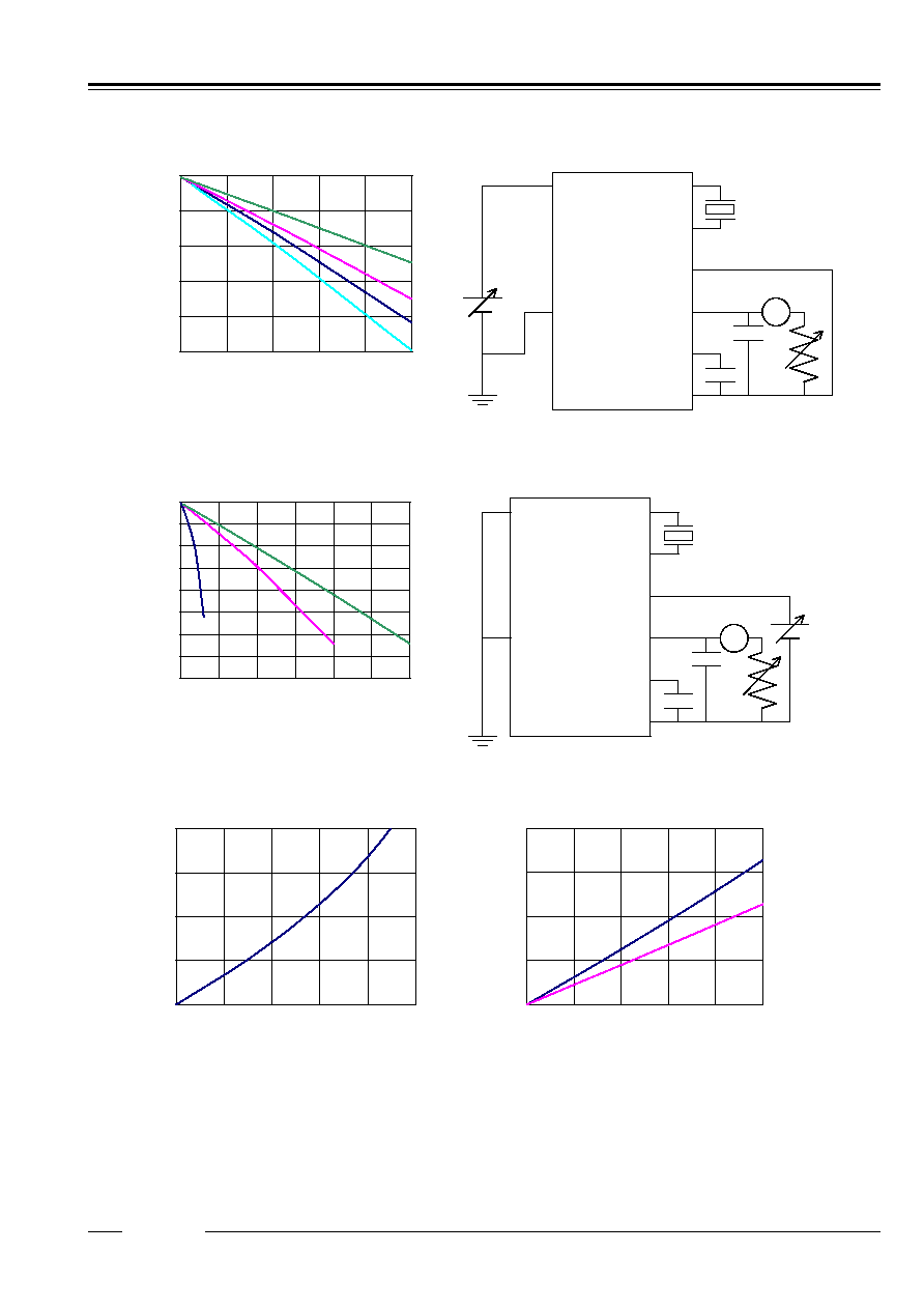
R2061 Series
12345
Rev.1.03 - 44 -
q
VCC-VDD(VDDOUT1) vs. Output load current (IOUT1) (R2061K01)
(Topt=25
∞
C) Test circuit
-0.5
-0.4
-0.3
-0.2
-0.1
0
0
2
4
6
8
10
Output load current IOUT1(mA)
VCC-
VDD(
V)
VCC
VSB
VDD
CIN
VSS
OSCIN
OSCOUT
/INTR
/VDCC
CE
SCLK
SIO
0.1
µ
F
0.1
µ
F
A
q
VSB-VDD(VDDOUT2) vs. Output load current (IOUT2) (R2061K01)
(Topt=25
∞
C) Test circuit
-0.8
-0.7
-0.6
-0.5
-0.4
-0.3
-0.2
-0.1
0
0
0.5
1
1.5
2
2.5
3
Output load current IOUT2(mA)
VSB-
VDD(
V)
VCC
VSB
VDD
CIN
VSS
OSCIN
OSCOUT
/INTR
/VDCC
CE
SCLK
SIO
0.1
µ
F
0.1
µ
F
A
q
VOL vs. IOL (/VDCC pin)
q
VOL vs. IOL (/INTR pin)
(Topt=25
∞
C, VSB=VCC=1.5v) (Topt=25
∞
C)
0
0.1
0.2
0.3
0.4
0
1
2
3
4
5
IOL(mA)
VOL(
v)
0
0.1
0.2
0.3
0.4
0
2
4
6
8
10
IOL(mA)
VOL(
v)
VCC=3V
VCC=5V
VSB=3V
VSB=2V
VSB=1V
VCC=5V
VCC=3V
VCC=2.5V
VCC=2.0V

R2061 Series
12345
Rev.1.03 - 45 -
s
Typical Software-based Operations
q
Initialization at Power-on
Start
*1)
Yes
No
VDET=0?
Warning Back-up
Battery Run-down
Set Oscillation Adjustment
Register and Control
Register 1 and 2, etc.
Power-on
*2)
*4)
*3)
PON=1?
Yes
No
*1)
After power-on from 0 volt, the process of internal initialization require a time span on 1sec, so that
access should be done after /VDCC turning to OFF(H).
*2)
The PON bit setting of 0 in the Control Register 1 indicates power-on from backup battery and not
from 0v. For further details, see "P.32
s
Power-on Reset, Oscillation Halt Sensing, and Supply
Voltage Monitoring
q
PON, /XST, and VDET ".
*3)
This step is not required when the supply voltage monitoring circuit is not used.
*4)
This step involves ordinary initialization including the Oscillation Adjustment Register and interrupt
cycle settings, etc.
q
Writing of Time and Calendar Data
Write to Time Counter and
Calendar Counter
*2)
CE
L
*3)
CE
H
*1)
*1) When writing to clock and calendar counters, do not insert CE=L until all
times from second to year have been written to prevent error in writing
time. (Detailed in "P.24
q
Considerations in Reading and Writing
Time Data under special condition
".
*2) Any writing to the second counter will reset divider units lower than the
second digits.
The R2061 may also be initialized not at power-on but in the process of
writing time and calendar data.

R2061 Series
12345
Rev.1.03 - 46 -
q
Reading Time and Calendar Data
(1) Ordinary Process of Reading Time and Calendar Data
Read from Time Counter
and Calendar Counter
*1)
CE
L
CE
H
*1)
(2) Basic Process of Reading Time and Calendar Data with Periodic Interrupt Function
*2)
Other Interrupt
Processes
Set Periodic Interrupt
Cycle Selection Bits
CTFG=1?
Read from Time Counter
and Calendar Counter
Yes
No
Control Register 2
(X1X1X011)
Generate Interrupt in CPU
*1)
*3)
*1) This step is intended to select the level mode as a
waveform mode for the periodic interrupt function.
*2) This step must be completed within 0.5 second.
*3) This step is intended to set the CTFG bit to 0 in the
Control Register 2 to cancel an interrupt to the CPU.
*1) When reading to clock and calendar counters, do not insert CE=L until all
times from second to year have been read to prevent error in reading
time. (Detailed in "P.24
q
Considerations in Reading and Writing
Time Data under special condition
".
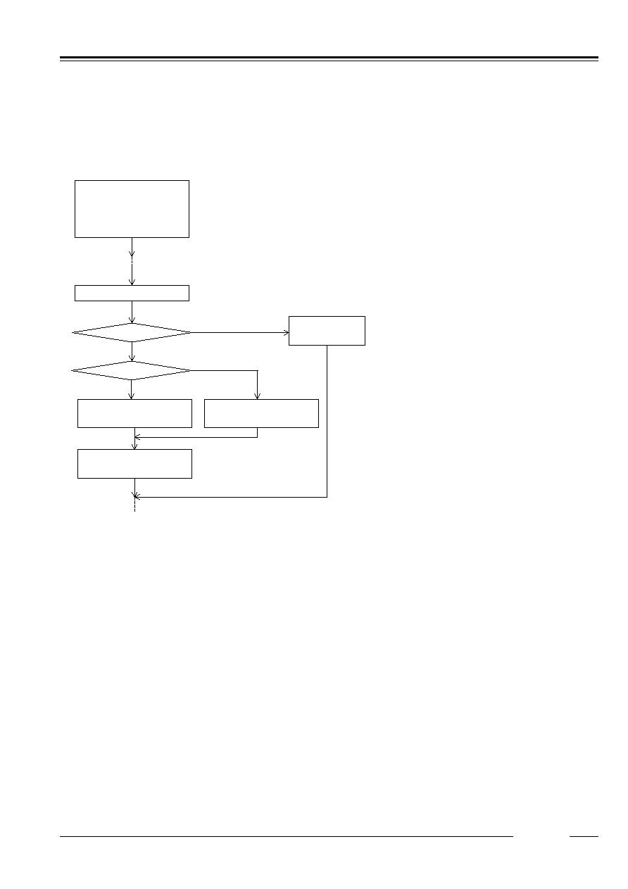
R2061 Series
12345
Rev.1.03 - 47 -
(3) Applied Process of Reading Time and Calendar Data with Periodic Interrupt Function
Time data need not be read from all the time counters when used for such ordinary purposes as time count
indication. This applied process can be used to read time and calendar data with substantial reductions in the
load involved in such reading.
For Time Indication in "Day-of-Month, Day-of-week, Hour, Minute, and Second" Format:
*2)
Other interrupts
Processes
Control Register 1
(XXXX0100)
Control Register 2
(X1X1X011)
Sec.=00?
Yes
No
Use Previous Min.,Hr.,
Day,and Day-of-week data
Generate interrupt to CPU
*1)
*3)
CTFG=1?
Control Register 2
(X1X1X011)
Yes
Read Min.,Hr.,Day,
and Day-of-week
*4)
No
*1) This step is intended to select the level
mode as a waveform mode for the
periodic interrupt function.
*2) This step must be completed within 0.5
sec.
*3) This step is intended to read time data
from all the time counters only in the
first session of reading time data after
writing time data.
*4) This step is intended to set the CTFG
bit to 0 in the Control Register 2 to
cancel an interrupt to the CPU.

R2061 Series
12345
Rev.1.03 - 48 -
q
Interrupt Process
(1) Periodic Interrupt
*2)
Other Interrupt
Processes
Set Periodic Interrupt
Cycle Selection Bits
CTFG=1?
Conduct
Periodic Interrupt
Yes
No
Control Register 2
(X1X1X011)
Generate Interrupt to CPU
*1)
(2) Alarm Interrupt
*3)
Other Interrupt
Processes
Set Alarm Min., Hr., and
Day-of-week Registers
WAFG or DAFG=1?
Conduct Alarm Interrupt
Yes
No
Control Register 2
(X1X1X101)
Generate Interrupt to CPU
*1)
WALE or DALE
0
*2)
WALE or DALE
1
*1) This step is intended to once disable the alarm
interrupt circuit by setting the WALE or DALE bits to 0
in anticipation of the coincidental occurrence of a
match between current time and preset alarm time in
the process of setting the alarm interrupt function.
*2) This step is intended to enable the alarm interrupt
function after completion of all alarm interrupt settings.
*3) This step is intended to once cancel the alarm
interrupt function by writing the settings of "X,1,X,
1,X,1,0,1" and "X,1,X,1,X,1,1,0" to the Alarm_W
Registers and the Alarm_D Registers, respectively.
*1) This step is intended to select the level mode as a
waveform mode for the periodic interrupt function.
*2) This step is intended to set the CTFG bit to 0 in
the Control Register 2 to cancel an interrupt to the
CPU.