 | ÐлекÑÑоннÑй компоненÑ: BA12002 | СкаÑаÑÑ:  PDF PDF  ZIP ZIP |
BA12001B / BA12003B / BA12003BF / BA12004B
BA12001B / BA12003B / BA12003BF / BA12004B
Standard ICs
High voltage, high current Darlington
transistor array
BA12001B / BA12003B / BA12003BF / BA12004B
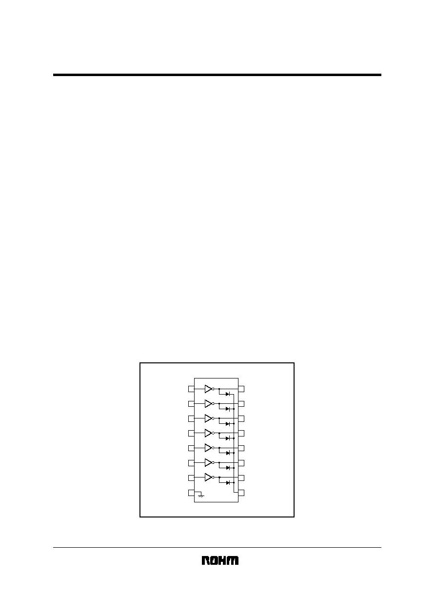
The BA12001B, BA12003B, BA12003BF, and BA12004B are high voltage, high current, high sustain voltage transistor
arrays consisting of seven circuits of Darlington transistors.
Because it incorporates built-in surge-absorbing diodes and base current-control resistors needed when using inductive
loads such as relay coils, attachments can be kept to a minimum.
With an output sustain voltage as high as 60V and an output current (sink current) of 500mA, this product is ideal for use
with various drivers and as an interface with other elements.
!
Applications
Drivers for LEDs, lamps, relays and solenoids
Interface with other elements
!
Features
1) High output current. (I
OUT
=500mA Max.)
2) High output sustain voltage. (V
OUT
=50V Max.)
3) Seven Darlington transistors built in.
4) Built-in surge-absorbing clamp diode.
(Note : Refer to the "Reference items when using in application." )
!
!
!
!
Block diagram
IN1
IN2
IN3
IN4
IN5
IN6
IN7
GND
OUT1
OUT2
OUT3
OUT4
OUT5
OUT6
OUT7
COM
8
16
15
14
13
12
11
10
1
2
3
4
5
6
7
9
BA12001B / BA12003B / BA12003BF / BA12004B
Standard ICs
!
!
!
!
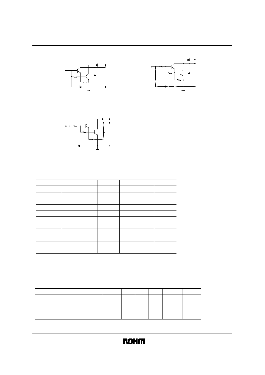
Internal circuit configuration
IN
COM
OUT
GND
3k
7.2k
Fig.1
BA12001B
IN
COM
OUT
GND
3k
7.2k
2.7k
Fig.2
BA12003B / BF
IN
COM
OUT
GND
3k
7.2k
10.5k
Fig.3
BA12004B
!
!
!
!
Absolute maximum ratings (Ta=25
°C)
Parameter
Symbol
Limits
Unit
V
CE
60
V
Input voltage
Input current
V
IN
-
0.5
+
30
V
other than BA12001B
BA12001B
DIP package
SOP package
I
IN
25
Output current
I
OUT
500
Ground pin current
I
GND
2.3
1
A
Power dissipation
Pd
1250
2
625
3
mW
Diode reverse voltage
V
R
60
V
Diode forward current
I
F
500
mA
Operating temperature
Topr
-
25
+
75
°C
Storage temperature
Tstg
-
55
+
150
°C
mA / unit
mA / unit
Power supply voltage
1 Pulse width
20ms, duty cycle
10%, same current for all 7 circuits
2 Reduced by 10mW for each increase in Ta of 1
°C over 25°C .
3 Reduced by 50mW for each increase in Ta of 1
°C over 25°C .
!
!
!
!
Recommended operating conditions (Ta=25
°C)
Parameter
Symbol
Min.
Typ.
Max.
Unit
Conditions
Output current
I
OUT
-
-
350
mA
Fig.9, 10
Power supply voltage
V
CE
-
-
55
V
-
Input voltage (excluding BA12001B)
V
IN
-
-
30
V
-
Input current (BA12001B only)
I
IN
-
-
25
-
mA / unit
BA12001B / BA12003B / BA12003BF / BA12004B
Standard ICs
!
!
!
!
Electrical characteristics (Ta=25
°C)
Parameter
Symbol
Min.
Typ.
Max.
Unit
Conditions
Output leakage current
I
L
-
0
10
µ
A
V
CE
= 60V
DC current transfer ratio
h
FE
1000
2400
-
V
Output saturation voltage
V
CE(sat)
-
0.94
1.1
V
1.14
1.3
1.46
1.6
Input voltage
V
IN
-
V
1.75
2
2.53
5
V
IN
-
V
1.91
2.4
2.75
6
V
IN
-
V
2.17
3.4
3.27
8
Input current
I
IN
-
mA
V
IN
= 3.85V
0.90
1.35
BA12003B / BF
BA12004B
BA12003B / BF
BA12004B
BA12003B / BF
BA12004B
BA12003B / BF
BA12004B
0.39
0.5
Diode reverse current
I
R
-
0
50
µ
A
V
R
= 60V
Diode forward voltage
V
F
-
1.73
2
V
I
F
= 350mA
Input capacitance
C
IN
-
30
-
pF
V
CE
= 2V, I
OUT
= 350mA
I
OUT
= 100mA, I
IN
= 250
µ
A
I
OUT
= 200mA, I
IN
= 350
µ
A
I
OUT
= 350mA, I
IN
= 500
µ
A
V
CE
= 2V, I
OUT
= 100mA
V
CE
= 2V, I
OUT
= 200mA
V
CE
= 2V, I
OUT
= 350mA
V
IN
= 5V
V
IN
= 0V, f = 1MHz
Note: Input voltage and input current for BA12001 vary based on external resistor.
!
!
!
!
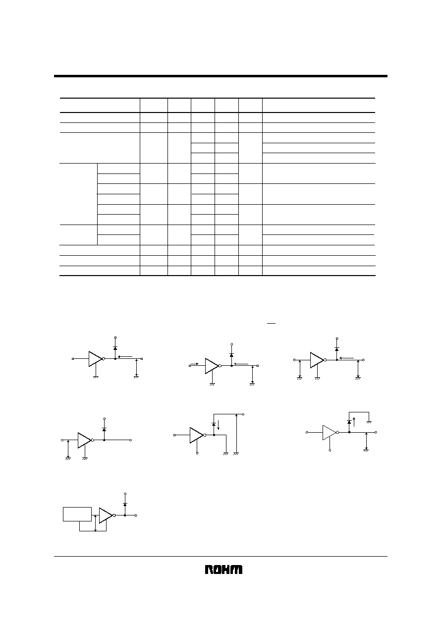
Measurement circuits
OPEN
OPEN
I
L
V
CE
(1) Output leakage current I
L
OPEN
I
I
I
O
V
CE
(sat)
(2) DC current transfer ratio
Output saturation voltage
I
I
I
O
V
CE
(sat)
h
FE
=
OPEN
I
O
V
CE
V
I
(3) Input voltage V
IN
OPEN
OPEN
V
I
(4) Input current I
IN
OPEN
I
R
V
R
OPEN
(5) Diode reverse current I
R
OPEN
OPEN
I
F
V
F
(6) Diode forward voltage I
F
OPEN
OPEN
V
I
L
O
H
I
Capacitance
bridge
f
TEST SIGNAL LEVEL 20mVrms
(7) Input capacitance C
IN
Fig.4
BA12001B / BA12003B / BA12003BF / BA12004B
Standard ICs
!
!
!
!
Application example
RY
(1) Relay driver
LED
(2) LED driver
Fig.5
!
!
!
!
Application notes
The BA12001B is a transistor array which can be directly coupled to a general logic circuit such as PMOS, CMOS, or
TTL.
A current limiting resistor needs to be connected in series with the input.
The BA12003B / BF can be coupled directly to TTL or CMOS output (when operating at 5V). In order to limit the input
current to a stable value, resistors are connected in series to each of the inputs.
The BA12004B is designed for direct coupling to CMOS or PMOS output using a 6 to 15V power supply voltage. In order
to limit the input current to a stable value, resistors are connected in series to each of the inputs.
The load for each of these products should be connected between the driver output and the power supply. To protect the
IC from excessive swing voltage, the COM pin (Pin 9) should be connected to the power supply.
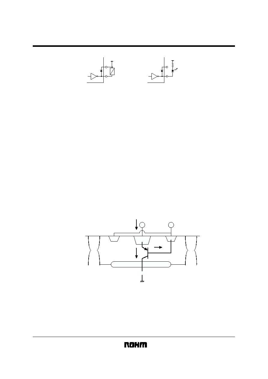
Fig.6 shows the configuration of the on-chip diode for surge absorption.
In the construction of the surge-absorbing diode,there is an N-P junction between the N-layer (N-well + BL) and the
substrate (P-sub) so that when the diode is on, current flows from the output pin to the substrate. In terms of the vertical
construction, this diode is configured similar to a PNP transistor. When using the surge-absorbing diode, take appropriate
measures regarding the thermal characteristics of the design considering the current that will be handled.
Also, if motor back-rush current or other conditions that will result continued surge current to flow to the surge-absorbing
diode can be foreseen, we strongly recommend connecting a Schottky barrier diode (or other type of diode with a low
foward voltage) in parallel with the surge-absorbing diode to construct a bypass route for the surge current.
ISO
P
ISO
P
B / L
IDi
Isub
N
+
P
+
In-flow current to the surge-absorbing diode
N
+
N
+
OUT
COM
P-sub
Fig.6 Vertical construction of the surge-absorbing diode
N-well
BA12001B / BA12003B / BA12003BF / BA12004B
Standard ICs
!
!
!
!
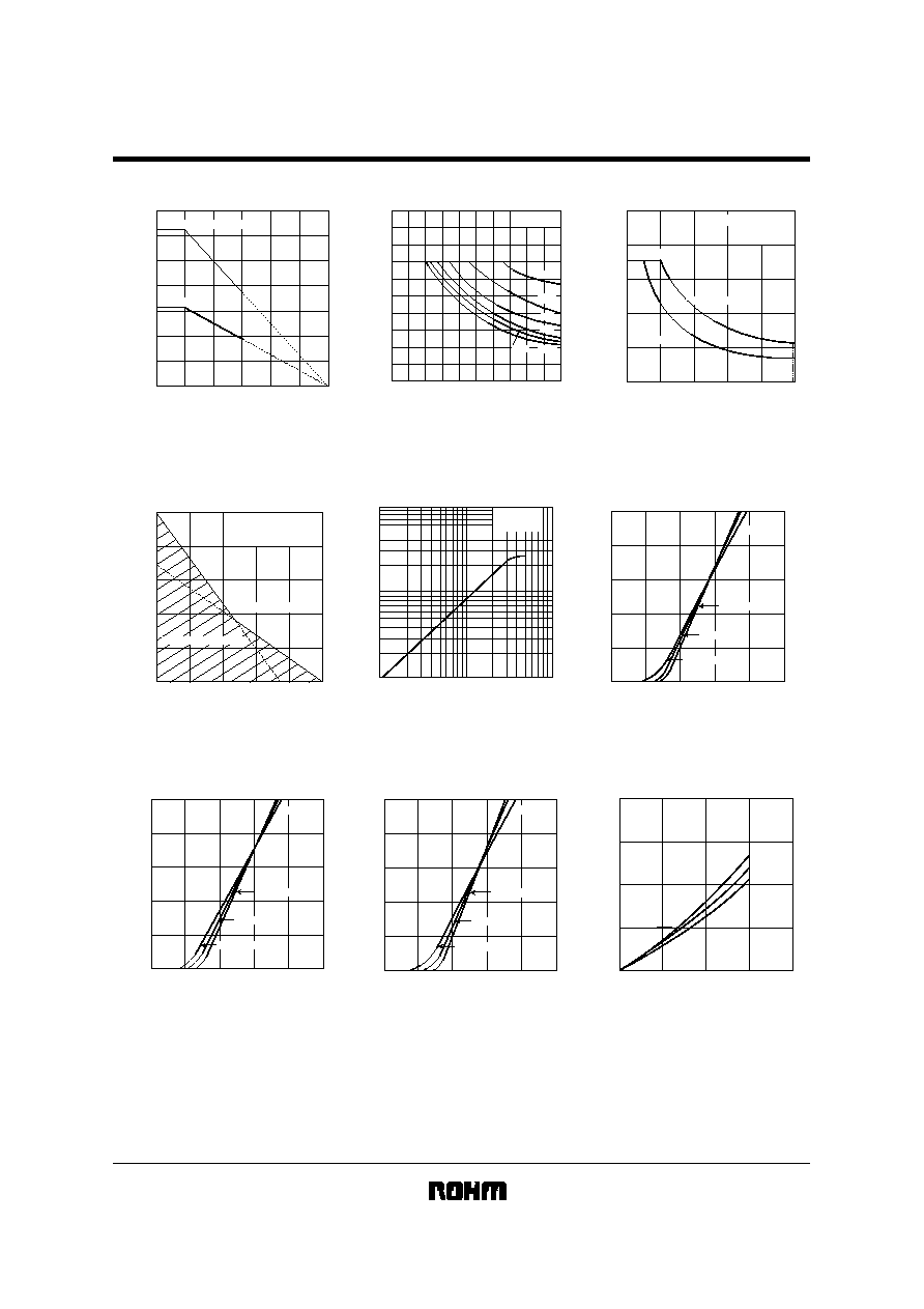
Electrical characteristic curves
POWER DISSIPATION : Pd (mW)
AMBIENT TEMPERATURE : Ta (°C)
1200
1250
1400
1000
800
600
625
200
0
25
50
75
100
125
150
Fig.7 Power dissipation vs. ambient
temperature
Other than BA12003BF
BA12003BF
400
OUTPUT CURRENT : I
O
(mA)
DUTY CYCLE : (%)
500
400
300
200
100
0
10 20 30 40 50 60 70 80 90 100
All series
2ch
4ch
5ch
7ch
6ch
3ch
Fig.8 Output conditions (I)
OUTPUT CURRENT : I
OUT
(mA)
DUTY CYCLE (%)
500
400
350
300
200
100
0
20
40
60
80
100
10% 20%
Ta = 75°C
Ta = 25°C
110mA
64mA
Fig.9 Output conditions (II)
When all circuits are on
All series
OUTPUT CURRENT: I
OUT
(mA)
SUPPLY VOLTAGE: V
CC
(V)
500
400
350
300
200
100
0
10
20
30
40
50
Max. usage conditions
Usage conditions range
Fig.10 Usage conditions range
per circuit
The shaded range should
never be exceeded under
any circumstances
DC CURRENT GAIN : h
FE
OUTPUT CURRET : I
OUT
(mA)
5000
2000
1000
100
200
500
Ta = 25°C
V
CE
= 2.0V
10
20
50
100
200
500
1000
Fig.11 DC current transfer ratio
vs. output current
OUTPUT CURRENT : I
OUT
(mA)
COLLECTOR TO EMITTER VOLTAGE : V
CE
(V)
500
400
300
0
100
200
0
0.5
1.0
1.5
2.0
2.5
Ta = 25°C
Ta = 80°C
Ta =
-
30°C
I
IN
= 250
µ
A
Fig.12 Output current vs. voltage
between collector and emitter
OUTPUT CURRENT : I
OUT
(mA)
COLLECTOR TO EMITTER VOLTAGE : V
CE
(V)
500
400
300
0
100
200
10
0.5
1.0
1.5
2.0
2.5
Ta = 25°C
Ta = 80°C
Ta =
-
30°C
I
IN
= 350
µ
A
Fig.13 Output current vs. voltage
between collector and emitter
OUTPUT CURRENT : I
OUT
(mA)
COLLECTOR TO EMITTER VOLTAGE : V
CE
(V)
500
400
300
0
100
200
0
0.5
1.0
1.5
2.0
2.5
Ta = 25°C
Ta = 80°C
Ta =
-
30°C
I
IN
= 500
µ
A
Fig.14 Output current vs. voltage
between collector and emitter
INPUT CURRENT : I
IN
(mA)
INPUT VOLTAGE : V
IN
(V)
20
15
10
0
5
10
20
30
40
Ta =
-
25°C
Ta = 25°C
Ta = 75°C
Fig.15 Input current vs. input
voltage (BA12003B / BF)
Document Outline