Äîêóìåíòàöèÿ è îïèñàíèÿ www.docs.chipfind.ru
BP5232-25A / BP5232-33A / BP5233-33A / BP5234-33A
Power Module
DC / DC converter
BP5232-25A / BP5232-33A / BP5233-33A /
BP5234-33A
The BP5232-25A, BP5232-33A, BP5233-33A and BP5234-33A are DC / DC converters that use PWM system and VIF
system. They contain control circuits, switching devices and coils, and operate by only connecting an I/O smoothing
capacitor.
With a high efficiency of power conversion, the modules are available in stand-alone SIP packages with no heat sink
required.
!
!
!
!
Applications
Power supplies for copiers, personal computers, facsimiles, industrial equipment, and AV eqipment
!
Features
1) High power conversion efficiency. (BP5233-33A : 93%)
2) Large output current.
3) Low current consumption with no load. (BP5233-33A : 200
µA Typ.)
4) High conversion efficiency. (85% at output current of 100mA)
5) Applicable to various purposes by fine-adjusting output voltage with external circuits.
6) Built-in ON / OFF switch.
7) Heat sink unnecessary.
!
Absolute maximum ratings (Ta=25
°C)
Parameter
Symbol
Limits
Unit
Input voltage
Output current
Operating temperature
Storage temperature
V
IN
I
O
Topr
Tstg
V
A
°
C
°
C
Derating required according to the input voltage and ambient temperature..
BP5232-25A BP5232-33A BP5233-33A BP5234-33A
7
2
2
3
4
-
20 ~
+
55
-
25 ~
+
80
!
Recommended operating conditions (Ta=25
°C)
Parameter
Input voltage
V
IN
4.5
5.5
5.0
Symbol
Min.
Typ.
Max.
Unit
V
BP5232-25A / BP5232-33A / BP5233-33A / BP5234-33A
Power Module
!
!
!
!
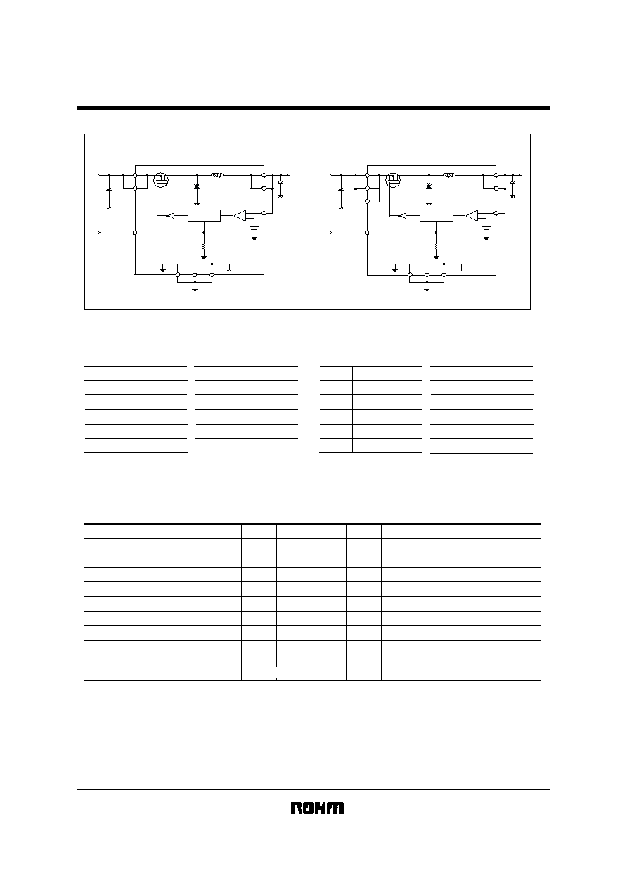
Block diagram
BP5232-25A / BP5232-33A
V
IN
=
5V
2
9
3
4
5
10
+
V
O
470
µ
F
+
1000
µ
F
Control circuit
Control circuit
7
6
ON / OFF
1
BP5233-33A / BP5234-33A
V
IN
=
5V
2
9
3
5
10
11
+
V
O
470
µ
F
+
1000
µ
F
7
6
CTL signal
CTL signal
ON / OFF
1
4
!
Pin descriptions
Pin description
Pin description
Pin description
Pin description
1
2
V
OUT
1
3
V
OUT
2
4
5
Pin 8 is removed.
Pin 8 is removed.
GND
Feed back
V
OUT
1
V
OUT
2
Feed back
GND
Pin No.
Pin No.
V
IN
1
V
IN
2
CTL
V
IN
1
V
IN
2
V
IN
3
CTL
6
7
9
10
GND
BP5232-25A , 5232-33A
1
2
3
4
5
GND
GND
Pin No.
Pin No.
6
7
9
10
11
GND
BP5233-33A , BP5234-33A
!
Electrical characteristics
BP5232-25A (Unless otherwise noted, V
lN
=5V, I
O
=1A, SW=1, Ta=25
°C)
Parameter
Symbol
Unit
Fig.1
Fig.1
Fig.1
Fig.1
Fig.1
Fig.1
Fig.1
Fig.1
Fig.1
Conditions
Measurement circuit
Min.
Typ.
Max.
V
IN
4.5
5
5.5
V
V
O
2.4
2.5
2.6
V
I
O
-
-
2
A
V
O
-
200
300
mV
I
O
=0.1A~2A
-
-
-
-
-
-
-
13
33
mV
PP
33
150
%
V
ON
1.8
89
V
V
OFF
0.3
V
SW=2
1
2
I
IN
84
µ
A
Input voltage
(Alternatively, when OPEN)
Output voltage
Output current
Load regulation
Output ripple voltage
Power conversion efficiency
CTL pin ON voltage
CTL pin OFF voltage
Current consuption at no load
1 Derating required according to the input voltage and ambient temperature.
2 Pulse noise not included.
BP5232-25A / BP5232-33A / BP5233-33A / BP5234-33A
Power Module
BP5232-33A (Unless otherwise noted, V
lN
=5V, I
O
=1A, SW=1, Ta=25
°C)
Parameter
Symbol
Unit
Fig.1
Fig.1
Fig.1
Fig.1
Fig.1
Fig.1
Fig.1
Fig.1
Fig.1
Conditions
Measurement circuit
Min.
Typ.
Max.
V
IN
4.5
5
5.5
V
V
O
3.17
3.3
3.43
V
I
O
-
-
2
A
V
O
-
200
300
mV
I
O
=0.1A~2A
-
-
-
-
-
-
-
16
42
mV
PP
33
150
%
V
ON
1.8
93
V
V
OFF
0.3
V
SW=2
1
2
I
IN
88
µ
A
Input voltage
(Alternatively, when OPEN)
Output voltage
Output current
Load regulation
Output ripple voltage
Power conversion efficiency
CTL pin ON voltage
CTL pin OFF voltage
Current consuption at no load
1 Derating required according to the input voltage and ambient temperature.
2 Pulse noise not included.
BP5233-33A (Unless otherwise noted, V
lN
=5V, I
O
=1.5A, SW=1, Ta=25
°C)
Parameter
Symbol
Unit
Fig.2
Fig.2
Fig.2
Fig.2
Fig.2
Fig.2
Fig.2
Fig.2
Fig.2
Conditions
Measurement circuit
Min.
Typ.
Max.
V
IN
4.5
5
5.5
V
V
O
3.17
3.3
3.43
V
I
O
-
-
3
A
V
O
-
200
300
mV
I
O
=0.1A~3A
-
-
-
-
-
-
-
16
42
mV
PP
33
150
%
V
ON
1.8
93
V
V
OFF
0.3
V
SW=2
1
2
I
IN
88
µ
A
Input voltage
(Alternatively, when OPEN)
Output voltage
Output current
Load regulation
Output ripple voltage
Power conversion efficiency
CTL pin ON voltage
CTL pin OFF voltage
Current consuption at no load
1 Derating required according to the input voltage and ambient temperature.
2 Pulse noise not included.
BP5234-33A (Unless otherwise noted, V
lN
=3.3V, I
O
=2A, SW=1, Ta=25
°C)
Parameter
Symbol
Unit
Fig.2
Fig.2
Fig.2
Fig.2
Fig.2
Fig.2
Fig.2
Fig.2
Fig.2
Conditions
Measurement circuit
Min.
Typ.
Max.
V
IN
4.5
5
5.5
V
V
O
3.17
3.3
3.43
V
I
O
-
-
4
A
V
O
-
200
300
mV
I
O
=0.1A~4A
-
-
-
-
-
-
-
16
42
mV
PP
33
150
%
V
ON
1.8
93
V
V
OFF
0.3
V
SW=2
1
2
I
IN
88
µ
A
Input voltage
(Alternatively, when OPEN)
Output voltage
Output current
Load regulation
Output ripple voltage
Power conversion efficiency
CTL pin ON voltage
CTL pin OFF voltage
Current consuption at no load
1 Derating required according to the input voltage and ambient temperature.
2 Pulse noise not included.
BP5232-25A / BP5232-33A / BP5233-33A / BP5234-33A
Power Module
!
!
!
!
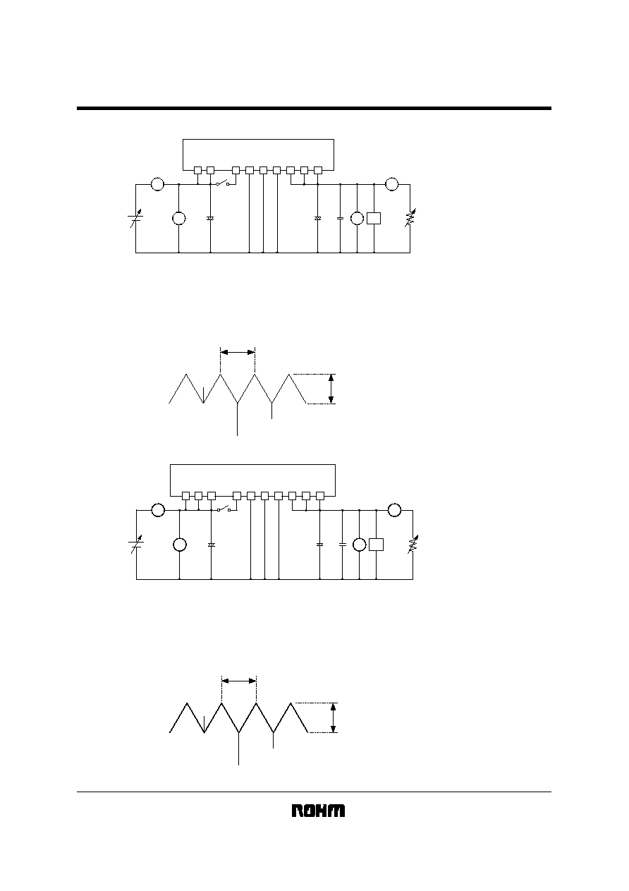
Measurement circuit
+
+
A
V
V
A
f
0.47
µ
F
470
µ
F / 50V
C3
T
Output ripple voltage
BP5232-25A / BP5232-33A
1000
µ
F / 50V
C2
Note that the output ripple voltage depends on the type and characteristics of the output capacitor.
Switching frequency=1 / T
A large ripple current flows to the input smoothing capacitor due
to the output load. Be minded to use within the allowable ripple
current of the capacitor.
The capacitor with a particularly low impedance is used as the
output smoothing capacitor C2 so as to suppress the output ripple
voltage. Select the capacitor according to the purpose of use in
each case.
f
: frequency counter
C1, C2 : Low impedance type
C3
: film capacitor
Fig.1
2
1
SW
C1
7
6
5
4
3
1
9
10
2
V
IN
V
O
+
+
7
6
5
4
3
2
1
A
V
V
A
f
0.47
µ
F
470
µ
F / 50V
C3
T
BP5233-33A / BP5234-33A
1000
µ
F / 50V
C2
Fig.2
9
10
2
1
SW
C1
11
V
IN
V
O
A large ripple current flows to the input smoothing capacitor due
to the output load. Be minded to use within the allowable ripple
current of the capacitor.
The capacitor with a particularly low impedance is used as the
output smoothing capacitor C2 so as to suppress the output ripple
voltage. Select the capacitor according to the purpose of use in
each case.
f
: frequency counter
C1, C2 : Low impedance type
C3
: film capacitor
Output ripple voltage
Note that the output ripple voltage depends on the type and characteristics of the output capacitor.
Switching frequency=1 / T
BP5232-25A / BP5232-33A / BP5233-33A / BP5234-33A
Power Module
!
!
!
!
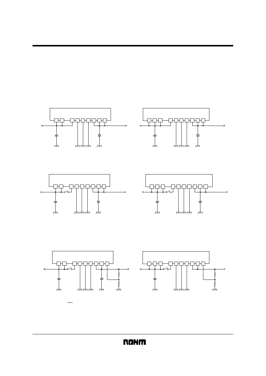
Circuit operation
(1) The basic application examples are shown in Fig.3. The externally installed parts are only the input and output
smoothing capacitors.
(2) Switching on and off the output voltage is allowed. The output can be switched off by making pin 7 to be low or open
(high impedance). (See Fig.4.)
(3) Fine adjustment of the output voltage is allowed. The fine adjustment of output voltage can be performed from pin 1
via the resistor by connecting the output terminal (pin 2, 3) and GND. (See Fig.5.)
Basic application
V
IN
V
O
BP5232-25A / BP5232-33A
+
+
Fig.3
1000
µ
F
470
µ
F
9
10
11
7
6
5
4
3
2
1
V
IN
V
O
BP5233-33A / BP5234-33A
+
+
1000
µ
F
470
µ
F
1
9
10
7
6
5
4
3
2
Output ON / OFF control
Fig.4
V
IN
SW
V
O
+
+
1000
µ
F
470
µ
F
V
O
V
IN
SW
BP5233-33A / BP5234-33A
+
+
1000
µ
F
470
µ
F
BP5232-25A / BP5232-33A
1
9
10
7
6
5
4
3
2
9
10
11
7
6
5
4
3
2
1
!
!
!
!
Application example
Output voltage fine adjustment
V
IN
V
O
'
V
O
' value setting equations
It is recommended that the output voltage should be adjusted
within the range of
±
10% of the rated output voltage, so that
the performance of the module can fully be exhibited.
V
O
R
2
R
1
+
+
R
1
+R
2
50k
V
O
'=V
O
1+
(
)
R
2
R
1
SW
1000
µ
F
470
µ
F
9
10
11
7
6
5
4
3
2
1
V
IN
V
O
'
V
O
R
2
R
1
BP5233-33A / BP5234-33A
+
SW
1000
µ
F
BP5232-25A / BP5232-33A
1
9
10
7
6
5
4
3
2
Fig.5
Document Outline