 | ÐлекÑÑоннÑй компоненÑ: BR24C21FV | СкаÑаÑÑ:  PDF PDF  ZIP ZIP |
Äîêóìåíòàöèÿ è îïèñàíèÿ www.docs.chipfind.ru
BR24C21 / BR24C21F / BR24C21FJ / BR24C21FV
Memory ICs
ID ROM for CRT display
BR24C21 / BR24C21F / BR24C21FJ / BR24C21FV
The BR24C21 series are 1kbits serial EEPROMs and support DDC1
TM
and DDC2
TM
interfaces for PLUG
&PLAY
displays.
!
Features
1) 128 x 8 bits serial EEPROM
2) Operating voltage range (2.5V
5.5V)
3) Completely implements DDC1
TM
/ DDC2
TM
interface
for monitor identification
Transmit-Only Mode
Recovery Mode
Bi-directional Mode
4) Page write function : 8 bytes
5) Low current consumption
Active (at 5V) : 1.5mA (Typ.)
Standby (at 5V) : 10
µA (Typ.)
6) DATA security
Write enable feature
Inhibit to WRITE at low Vcc
7) Compact packages
8) High reliability fine pattern CMOS technology
9) Rewriting possible up to 100,000 times
10) Data can be stored for ten years without corruption
11) Noise filters at SCL, SDA and VCLK pins
!
!
!
!
Absolute maximum ratings (Ta=25
°C)
Parameter
Symbol
Limits
Unit
Supply voltage
-
0.3
~
+
6.5
V
Power disssipation
mW
Storage temperature range
-
65
~
+
125
°
C
Operating temperature range
°
C
Terminal voltage
-
V
-
40
~
+
85
V
CC
-
0.3
~V
CC
+
0.3
Pd
Tstg
Topr
1
450(SOP8)
800(DIP8)
2
2
450(SOP-J8)
3
350(SSOP-B8)
1 Degradation is done at 8.0mW/
°
C for operation above 25
°
C.
2 Degradation is done at 4.5mW/
°
C for operation above 25
°
C.
3 Degradation is done at 3.5mW/
°
C for operation above 25
°
C.
!
!
!
!
Recommended operating conditions (Ta=25
°C)
Parameter
Symbol
Limits
Unit
Supply voltage
V
Input voltage
V
IN
V
V
CC
0
~V
CC
2.5
~5.5
BR24C21 / BR24C21F / BR24C21FJ / BR24C21FV
Memory ICs
!
!
!
!
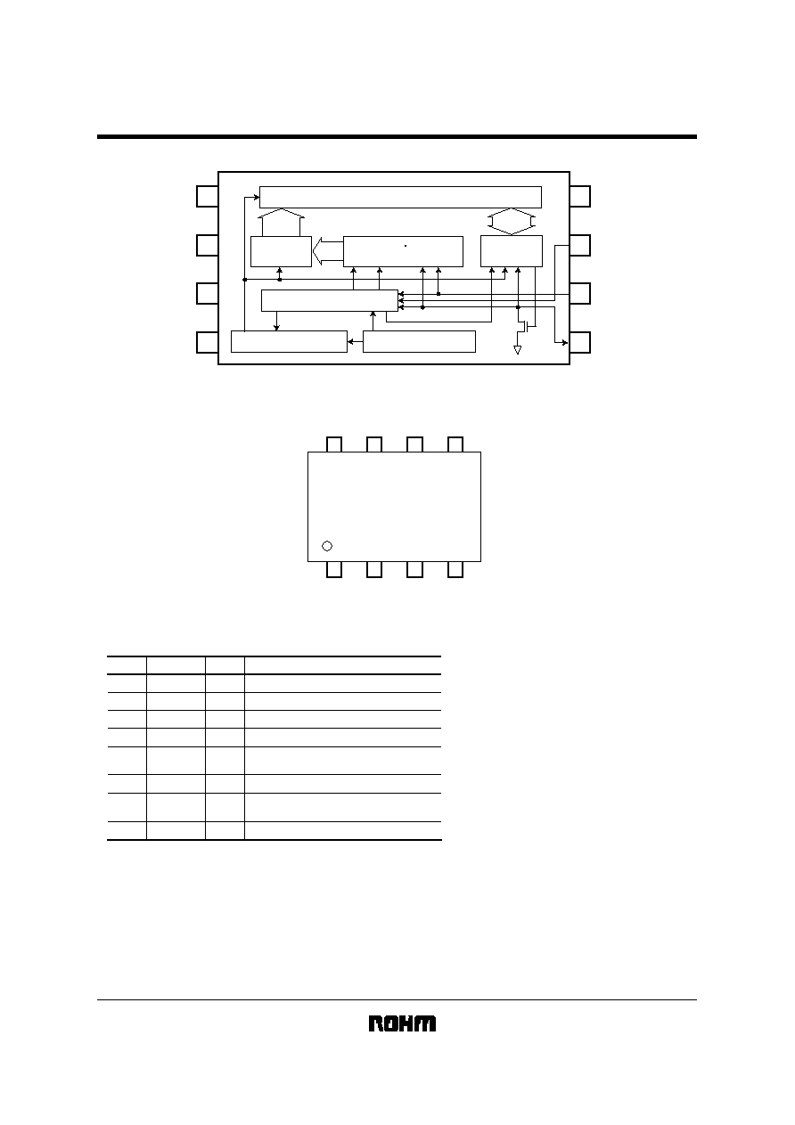
Block diagram
1
N.C.
N.C.
2
N.C.
3
GND
4
V
CC
8
VCLK
7
6
SCL
SDA
5
1kbits EEPROM array
Control logic
High voltage generator
Vcc level detecter
7bits
8bits
ACK
STOP
START
Address
decoder
Slave word
address register
7bits
Data
register
!
!
!
!
Pin assignment
BR24C21
BR24C21F
BR24C21FJ
BR24C21FV
V
CC
N.C.
VCLK
N.C.
SCL
N.C.
SDA
GND
1
2
3
4
5
6
7
8
!
!
!
!
Pin descriptions
5
6
Serial clock input for Bi-directional Mode
7
8
1
No connection
4
I / O
Pin No.
SCL
N.C.
GND
Pin name
Function
-
2
No connection
N.C.
-
3
No connection
N.C.
-
Power supply
V
CC
-
-
I
Clock input (Transmit-Only Mode)
Write enable (Bi-directional Mode)
VCLK
I
Ground (0V)
SDA
I / O
Slave and word address,
serial data input, serial data output
An open drain output requires a pull-up resistor.
BR24C21 / BR24C21F / BR24C21FJ / BR24C21FV
Memory ICs
!
!
!
!
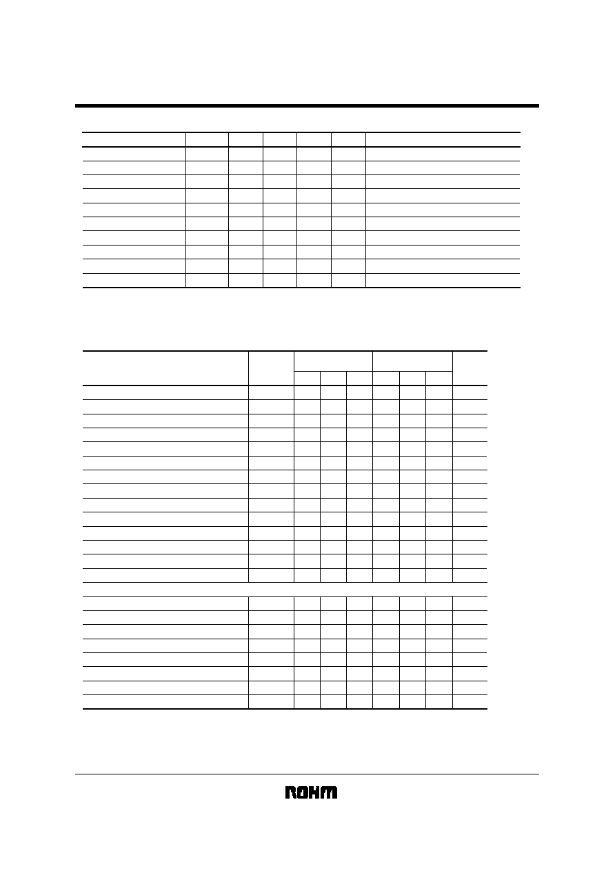
Electrical characteristics (Unless otherwise noted, Ta=
-4085°C, V
CC
=2.5
5.5V)
Parameter
Symbol
Min.
Typ.
Max.
Unit
Conditions
V
IH1
-
-
V
V
IL1
-
-
0.3V
CC
V
V
OL
-
-
0.4
V
Input leakage current
I
LI
-
1
µ
A
SCL,
VCLK, V
IN
=
0V
~V
CC
Output leakage current
I
LO
-
1
-
1
-
1
µ
A
Operating current
I
CC
-
3.0
mA
Standby current
I
SB
-
-
10
100
µ
A
0.7V
CC
SCL, SDA
SCL, SDA
SDA, I
OL
=
3.0mA
V
CC
=
5.5V, f
SCL
=
400kHz
SDA, V
OUT
=
0V
~V
CC
"HIGH" input volatge1
"LOW" input volatge1
V
IH2
-
-
V
V
IL2
-
-
0.8
V
2.0
VCLK, V
CC
4.0V
VCLK
"HIGH" input volatge2
"LOW" input volatge2
V
IL3
-
-
0.2V
CC
V
VCLK, V
CC
<
4.0V
"LOW" input volatge3
"LOW" output volatge
V
CC
=
5.5V, SDA
=
SCL
=
V
CC
,
VCLK
=
GND
1
1 Transmit-Only Mode
...
After the power is on, the BR24C21, BR24C21F, BR24C21FJ and BR24C21FV are in Standby state without providing the clock on the VCLK pin.
After the VCLK pin is provided the clock, the device is switched from Standby to Transmit-Only Mode, and the operating current runs.
Bi-directional Mode
...
The BR24C21, BR24C21F, BR24C21FJ and BR24C21FV are in Standby state after each command is porformed.
!
!
!
!
Operating timing characteristics (Unless otherwise noted, Ta=
-4085°C, V
CC
=2.5
5.5V)
Parameter
Symbol
Fast-mode
Vcc
=
2.5~5.5V
Standard-mode
Vcc
=
2.5~5.5V
Unit
f
SCL
kHz
t
HIGH
Noise erase valid time (SCL and SDA)
t
I
µ
s
Data clock "HIGH" time
SCL frequency
µ
s
Data clock "LOW" time
t
LOW
µ
s
SDA/SCL rise time
t
R
µ
s
SDA/SCL fall time
t
F
µ
s
Start condition hold time
t
HD
: STA
µ
s
Start condition setup time
t
SU
: STA
µ
s
Input data hold time
t
HD
: DAT
ns
Input data setup time
t
SU
: DAT
ns
Output data delay time (SCL)
t
PD
µ
s
Stop condition setup time
t
SU
: STO
µ
s
Bus open time before start or transfer
t
BUF
µ
s
t
WR
Min.
-
0.6
-
1.3
-
-
0.6
0.6
0
100
-
0.6
1.3
-
Typ.
-
-
-
-
-
-
-
-
-
-
-
-
-
-
Max.
400
-
0.1
-
0.3
0.3
-
-
-
-
0.9
-
-
10
Min.
-
4.0
-
4.7
-
-
4.0
4.7
0
250
-
4.0
4.7
-
Typ.
-
-
-
-
-
-
-
-
-
-
-
-
-
-
Max.
100
-
t
VHIGH
VCLK
"HIGH" time
µ
s
0.6
-
-
4.0
-
-
0.1
-
1.0
0.3
-
-
-
-
3.5
Output data delay time (VCLK)
t
VPD
µ
s
-
-
1.0
-
-
2.0
-
-
10
ms
Internal write cycle time
Noise erase valid time (VCLK)
t
VI
µ
s
<
Transmit-Only Mode
>
VCLK
"LOW" time
t
VLOW
µ
s
Transmit-Only powerup time
t
VPU
µ
s
VCLK hold time
t
VHD
µ
s
VCLK setup time
t
VSU
µ
s
-
1.3
0
0.6
0
-
-
-
-
-
0.1
-
-
-
-
-
4.7
0
4.0
0
-
-
-
-
-
0.1
-
-
Mode transition time
t
VHZ
µ
s
-
-
0.5
-
-
1.0
-
-
BR24C21 / BR24C21F / BR24C21FJ / BR24C21FV
Memory ICs
!
!
!
!
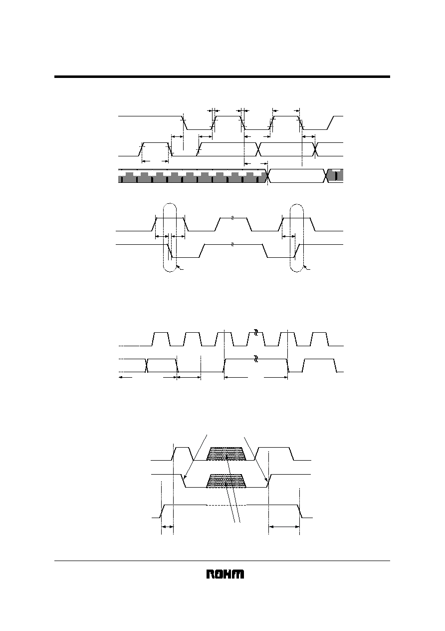
Timing charts
SYNCHRONOUS DATA TIMING
t
BUF
t
PD
t
HIGH
t
HD :
STA
t
LOW
t
F
t
R
SCL
START BIT
STOP BIT
SCL
SDA
t
SU
: DAT
t
HD
: DAT
t
SU
: STO
t
HD
: STA
t
SU
: STA
SDA
(OUT)
SDA
(IN)
Fig.7
·SDA data is latched into the chip at the rising edge of the SCL clock.
·Output data toggles at the falling edge of the SCL clock.
WRITE CYCLE TIMING
ACK
D0
(n)
t
WR
SDA
SCL
START CONDITION
STOP CONDITION
WRITE DATA
Fig.8
WRITE ENABLE TIMING
Fig.9
SDA
t
VSU
t
VHD
WRITE COMMAND
VCLK
SCL
START BIT
STOP BIT
BR24C21 / BR24C21F / BR24C21FJ / BR24C21FV
Memory ICs
!
!
!
!
Circuit operation
The BR24C21, BR24C21F, BR24C21FJ and BR24C21FV operate in two modes, Transmit-Only Mode and Bi-directional
Mode. The devices operate in Transmit-Only Mode when they will power up. In this mode, the devices transmit data on
the SDA pin with the VCLK clock. This mode is continued by providing a valid high to low transition on the SCL pin.
The devices can be switched into Bi-directional Mode by providing a valid high to low transition on the SCL pin. They
begin to count the VCLK clock at once. If the VCLK counter reaches 128 clock without the command for Bi-directional
Mode, the device revert to Transmit-Only Mode. (Recovery function) If the devices are received the command for Bi-
directional Mode and respond with an Acknowledge before the VCLK counter reaches 128 clock, it is impossible to revert
to Transmit-Only Mode. (The way to switch Bi-directional Mode to Transmit-Only Mode is that the power down again.)
* When the power is on, the SCL pin set to V
CC
(High level).
(1) Transmit-Only Mode
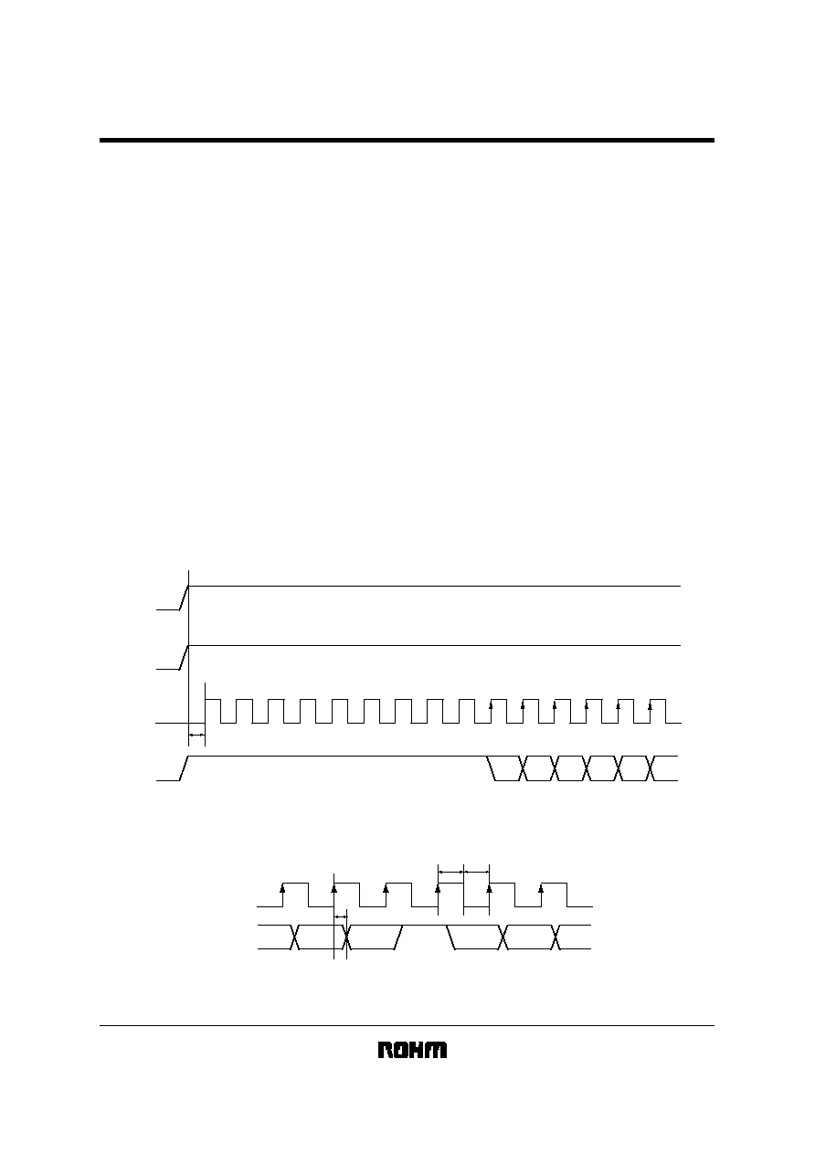
·After the power is on, the BR24C21, BR24C21F, BR24C21FJ and BR24C21FV are in Transmit-Only Mode. In this
mode, the data can be output by providing the clock on the VCLK pin.
·When the power is on, the SCL pin set to V
CC
(High level).
·The state of SDA is high-impedance during input of the first 9 clocks, and a data is output starting with the 10th rising
clock edge on VCLK. After the power is on, the output data is as follow
00h address data
01h address data 02h address data ...
The address is incremented by one with every 9 clock of VCLK. All address is output in this mode. When the counter
reaches the last address, the next output data is 00h address data.
·In the mode, the NULL bit (High data) is output between the address data and the next address data.
·The read operation in Transmit-Only Mode can be started after the power stabilized.
Fig.10 TRANSMIT-ONLY MODE
00h ADDRESS DATA
SDA
VCLK
SCL
V
CC
t
VPU
D3
D4
D5
D6
D7
1
9
10
Fig.11 NULL BIT
ADDRESS n
DATA
ADDRESS n+1
DATA
NULL BIT
DATA=1
SDA
VCLK
D1
D0
D7
D6
t
VPD
t
VHIGH
t
VLOW
Document Outline