BR24L32-W / BR24L32F-W / BR24L32FJ-W / BR24L32FV-W
Memory ICs
1/25
4k
×
8 bit electrically erasable PROM
BR24L32-W / BR24L32F-W / BR24L32FJ-W
BR24L32FV-W
The BR24L32-W series is 2-wire (I
2
C BUS type) serial EEPROMs which are electrically programmable.
I
2
C BUS is a registered trademark of Philips.
Applications
General purpose
Features
1) 4k registers
×
8 bits serial architecture.
2) Single power supply (1.8V to 5.5V).
3) Two wire serial interface.
4) Automatic erase.
5) 32byte Page Write Mode.
6) Low power consumption.
Write
(5V) : 1.5mA (Typ.)
Read (5V) : 0.2mA (Typ.)
Standby (5V) : 0.1
µ
A (Typ.)
7) DATA security
Write protect feature (WP pin).
Inhibit to WRITE at low V
CC
.
8) Small package - - - DIP8 / SOP8 / SSOP-B8 pin
9) High reliability EEPROM with Double-Cell structure.
10) High reliability fine pattern CMOS technology.
11) Endurance : 1,000,000 erase / write cycles
12) Data retention : 40 years
13) Filtered inputs in SCL,SDA for noise suppression.
14) Initial data FFh in all address.
Absolute maximum ratings (Ta=25
°
C)
Parameter
Symbol
Limits
Unit
Supply voltage
-
0.3 to
+
6.5
V
Power dissipation
mW
Storage temperature
-
65 to
+
125
°
C
Operating temperature
°
C
Terminal voltage
-
V
-
40 to
+
85
V
CC
-
0.3 to V
CC
+
0.3
Pd
Tstg
Topr
1
450(SOP8)
800(DIP8)
2
3
300(SSOP-B8)
1 Degradation is done at 8.0mW/
°
C for operation above 25
°
C.
2,3 Degradation is done at 4.5mW/
°
C for operation above 25
°
C.
4 Degradation is done at 3.0mW/
°
C for operation above 25
°
C.
450(SOP-J8)
4
BR24L32-W / BR24L32F-W / BR24L32FJ-W / BR24L32FV-W
Memory ICs
2/25
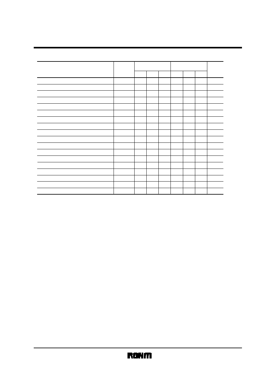
Recommended operating conditions (Ta=25
°
C)
Parameter
Symbol
Limits
Unit
Supply voltage
V
Input voltage
V
IN
V
V
CC
0 to V
CC
1.8 to 5.5
DC operating characteristics (Unless otherwise specified Ta
=-
40 to 85
°
C, V
CC
=
1.8 to 5.5V)
Parameter
Symbol
Min.
Typ.
Max.
Unit
Conditions
V
IH1
-
-
V
V
IL1
-
-
0.3V
CC
V
V
OL2
-
-
0.2
V
Input leakage current
I
LI
-
1
µ
A
V
IN
=
0V to V
CC
Output leakage current
I
LO
-
1
-
1
-
1
µ
A
Operating current
I
CC2
-
0.5
mA
Standby current
I
SB
-
-
I
CC1
-
3.0
mA
-
-
2.0
µ
A
0.7V
CC
2.5V V
CC
5.5V
2.5V V
CC
5.5V
I
OL
=
0.7mA, 1.8V V
CC
5.5V, (SDA)
V
CC
=
5.5V, f
SCL
=
400kHz
Random Read, Current Read,
Sequential Read
V
OUT
=
0V to V
CC
"HIGH" input volatge 1
"LOW" input volatge 1
V
IH2
-
-
V
V
IL2
-
-
0.2V
CC
V
0.8V
CC
1.8V V
CC
2.5V
1.8V V
CC
2.5V
"HIGH" input volatge 2
"LOW" input volatge 2
V
OL1
-
-
0.4
V
I
OL
=
3.0mA, 2.5V V
CC
5.5V, (SDA)
"LOW" output volatge 2
"LOW" output volatge 1
V
CC
=
5.5V, SDA,SCL
=
V
CC
,
A0,A1,A2
=
GND, WP
=
GND
V
CC
=
5.5V, f
SCL
=
400kHz, t
WR
=5ms,
Byte Write, Page Write
This product is not designed for protection against radioactive rays.
=
<
=
<
=
<
=
<
=
<
=
<
=
<
=
<
=
<
=
<
=
<
=
<
BR24L32-W / BR24L32F-W / BR24L32FJ-W / BR24L32FV-W
Memory ICs
3/25
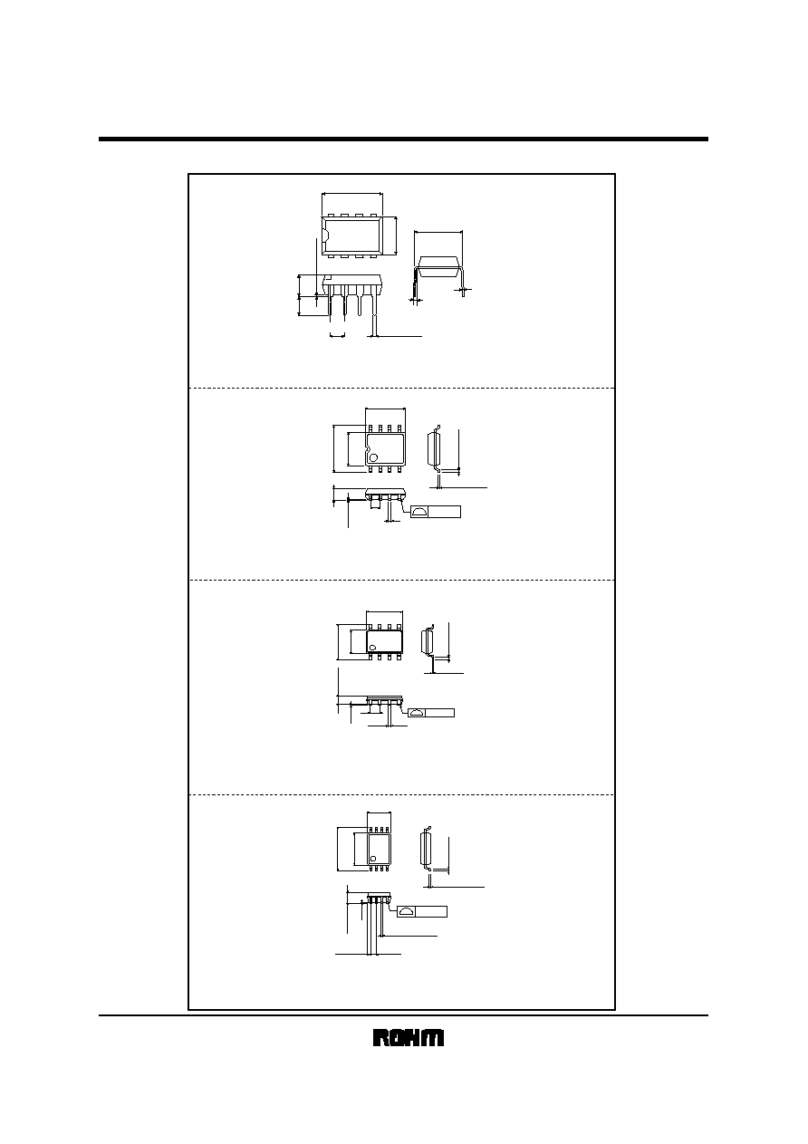
Dimension
Fig.1(a) PHYSICAL DIMENSION (Units : mm) DIP8 (BR24L32-W)
0.5
±
0.1
3.2
±
0.2
3.4
±
0.3
8
5
1
4
9.3
±
0.3
6.5
±
0.3
0.3
±
0.1
0.51Min.
2.54
0
°
~ 15
°
7.62
0.3Min.
0.15
±
0.1
0.4
±
0.1
0.11
6.2
±
0.3
4.4
±
0.2
5.0
±
0.2
8
5
4
1
1.27
1.5
±
0.1
0.1
Fig.1(b) PHYSICAL DIMENSION (Units : mm) SOP8 (BR24L32F-W)
5
4
8
1
0.1
6.4
±
0.3
4.4
±
0.2
3.0
±
0.2
0.22
±
0.1
1.15
±
0.1
0.65
(0.52)
0.15
±
0.1
0.3Min.
0.1
Fig.1(d) PHYSICAL DIMENSION (Units : mm) SSOP-B8 (BR24L32FV-W)
0.1
0.45Min.
0.42±0.1
4.9±0.2
8
5
4
1 2 3
1.27
7 6
0.2±0.1
0.175
6.0±0.3
3.9±0.2
1.375±0.1
Fig.1(c) PHYSICAL DIMENSION (Units : mm) SOP-J8 (BR24L32FJ-W)
BR24L32-W / BR24L32F-W / BR24L32FJ-W / BR24L32FV-W
Memory ICs
4/25
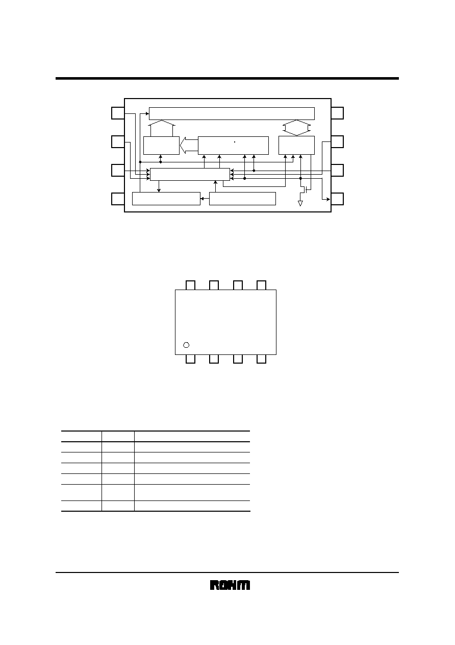
Block diagram
1
A0
A1
2
A2
3
GND
4
V
CC
8
WP
7
6
SCL
SDA
5
32kbit EEPROM array
Control logic
High voltage generator
Vcc level detect
12bit
8bit
ACK
STOP
START
Address
decoder
Slave word
address register
12bits
Data
register
Fig.2 BLOCK DIAGRAM
Pin configuration
BR24L32-W
BR24L32F-W
BR24L32FJ-W
BR24L32FV-W
V
CC
A0
WP
A1
SCL
A2
SDA
GND
1
2
3
4
5
6
7
8
Fig.3 PIN LAYOUT
Pin name
Write protect input
Power supply
Function
Ground (0V)
Slave address set
Serial clock input
SDA
V
CC
A0, A1, A2
Pin name
GND
WP
SCL
I / O
-
-
IN
IN
IN
IN / OUT
Slave and word address,
serial data input, serial data output
An open drain output requires a pull-up resistor.
BR24L32-W / BR24L32F-W / BR24L32FJ-W / BR24L32FV-W
Memory ICs
5/25
AC operating characteristics (Unless otherwise specified Ta
=-
40 to 85
°
C, V
CC
=
1.8 to 5.5V)
Parameter
Symbol
Fast-mode
2.5V
Vcc
5.5V
Standard-mode
1.8V
Vcc
5.5V
Unit
fSCL
kHz
tHIGH
Noise spike width (SDA and SCL)
tWR
tI
ms
Data clock "HIGH" period
Clock frequency
µ
s
Data clock "LOW" period
tLOW
µ
s
SDA and SCL rise time
Not 100% tested.
tR
µ
s
SDA and SCL fall time
tF
µ
s
Start condition hold time
tHD:STA
µ
s
Start condition setup time
tSU:STA
µ
s
Input data hold time
tHD:DAT
ns
Input data setup time
tSU:DAT
ns
Output data delay time
Output data hold time
tPD
µ
s
Stop condition setup time
tDH
µ
s
Bus free time
tSU:STO
µ
s
tBUF
Min.
-
0.6
-
-
1.2
-
-
0.6
0.6
0
100
0.1
0.1
0.6
1.2
Typ.
-
-
-
-
-
-
-
-
-
-
-
-
-
-
-
Max.
400
-
5
-
0.3
0.3
-
-
-
-
0.9
-
-
-
Min.
-
4.0
-
-
4.7
-
-
4.0
4.7
0
250
0.2
0.2
4.7
4.7
Typ.
-
-
-
-
-
-
-
-
-
-
-
-
-
-
-
Max.
100
-
tSU:WP
WP high period
µ
s
0.1
-
-
0.1
-
-
5
0.1
-
1.0
0.3
-
-
-
-
3.5
WP setup time
tHD:WP
ns
µ
s
0
-
-
0.1
0
-
-
-
-
-
µ
s
Write cycle time
WP hold time
tHIGH:WP
µ
s
1.0
-
-
1.0
-
-
=
<
=
<
=
<
=
<