 | ÐлекÑÑоннÑй компоненÑ: BR9010-W | СкаÑаÑÑ:  PDF PDF  ZIP ZIP |
þÿØ�^¦0¹0¤0Ã0Á0ó0°0À0¤0ª0ü0É

BR9010-W / F-W / FV-W / RFV-W / RFVM-W / BR9020-W / F-W / FV-W /
Memory IC
RFV-W / RFVM-W / BR9040-W / F-W / FV-W / RFV-W / RFVM-W
1/14
1k, 2k, 4k, bit EEPROMs for direct
connection to serial ports
BR9010-W / BR9010F-W / BR9010FV-W /
BR9010RFV-W / BR9010RFVM-W
BR9020-W / BR9020F-W / BR9020FV-W /
BR9020RFV-W / BR9020RFVM-W
BR9040-W / BR9040F-W / BR9040FV-W /
BR9040RFV-W / BR9040RFVM-W
The BR90XX series are serial EEPROMs that can be connected directly to a serial port and can be erased and written
electrically. Writing and reading is perfomed in word units, using four types of operation commands. Communication
occurs through CS, SK, DI, and DO pins, WC pin control is used to initiate a write disabled state, enabling these
EEPROMs to be used as one-time ROMs. During writing operation is checked via the internal status check.
Application
General-Purpose
Features
1) BR9010-W / F-W / FV-W / RFV-W / RFVM-W (1k bit) : 64 words
×
16bit
BR9020-W / F-W / FV-W / RFV-W / RFVM-W (2k bit) : 128words
×
16bit
BR9040-W / F-W / FV-W / RFV-W / RFVM-W (4k bit) : 256words
×
16bit
2) Single power supply.
3) Serial data I/O.
4) Self-timed programming cycle with auto-erase.
5) Low supply current.
Active (5V) : 2mA (max.)
Standby (5V) : 3
µ
A (max.) (CMOS INPUT)
6) Noise filter on the SK pin. Write protection when the supply is low.
7) Write protection by WC pin.
8) Space Saving DIP8/SOP8/SSOP-B8/MSOP8pin Packages.
9) 100,000 erase/ write cycles endurance.
10) Provide 10 years of date retention.
11) Easy connection to serial port.
12) "FFFFh" stored in all address on shipped.
BR9010-W / F-W / FV-W / RFV-W / RFVM-W / BR9020-W / F-W / FV-W /
Memory IC
RFV-W / RFVM-W / BR9040-W / F-W / FV-W / RFV-W / RFVM-W
2/14
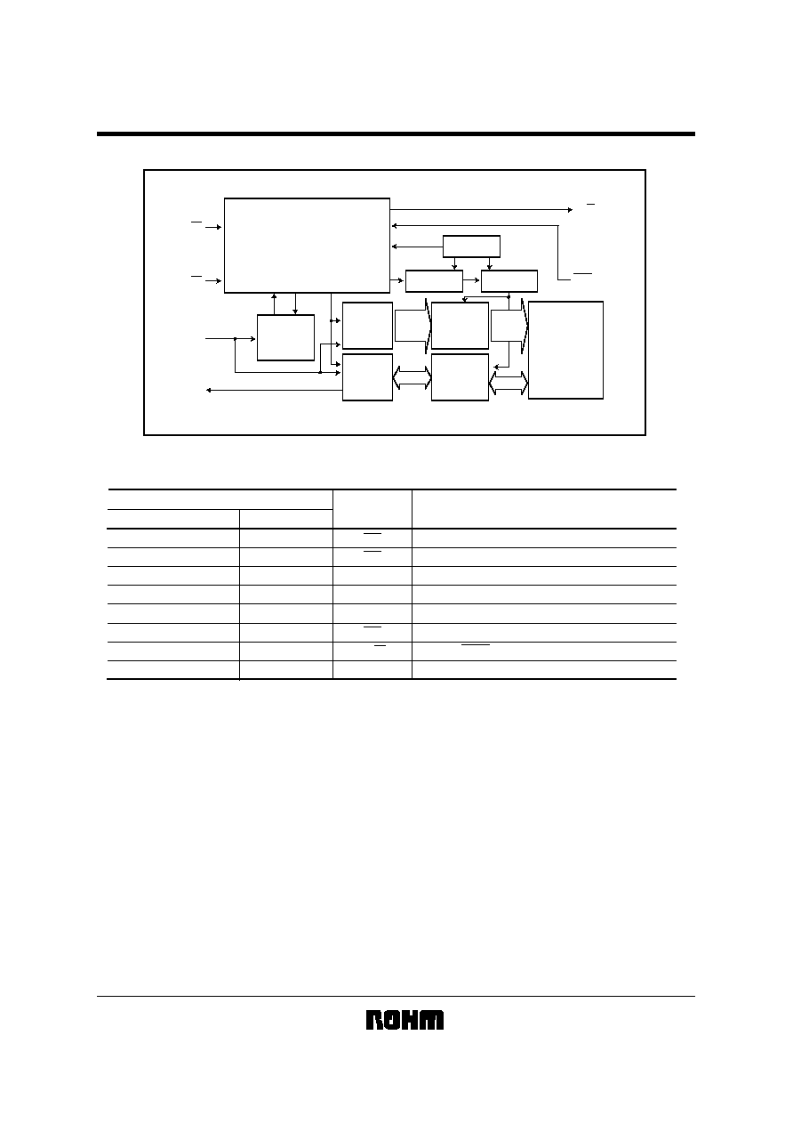
Block diagram
16bit
16bit
CS
R / B
WC
SK
DI
DO
6bit
BR9010
7bit
BR9020
8bit
BR9040
6bit
BR9010
7bit
BR9020
8bit
BR9040
Command decode
Control
Clock generation
Write disable
Power supply
voltage detector
High voltage
generator
Address
decoder
R / W
amplifier
Address
buffer
Command
register
Data
register
1,024bit
BR9010
2,048bit
BR9020
4,096bit
BR9040
EEPROM
array
Terminal Function
3
4
5
6
7
8
1
2
1
2
3
4
5
6
7
8
CS
SK
DI
DO
GND
WC
R / B
V
CC
BR90xx-W/RFV-W/RFVM-W
BR90xxF-W/FV-W
Pin No.
Pin name
Chip Select Input
Serial Date Clock Input
Serial Date Input (Op code, address)
Ground (0V)
Write Control Input
READY/ BUSY Status Output
Power Supply
Serial Date Output
Function
BR9010-W / F-W / FV-W / RFV-W / RFVM-W / BR9020-W / F-W / FV-W /
Memory IC
RFV-W / RFVM-W / BR9040-W / F-W / FV-W / RFV-W / RFVM-W
3/14
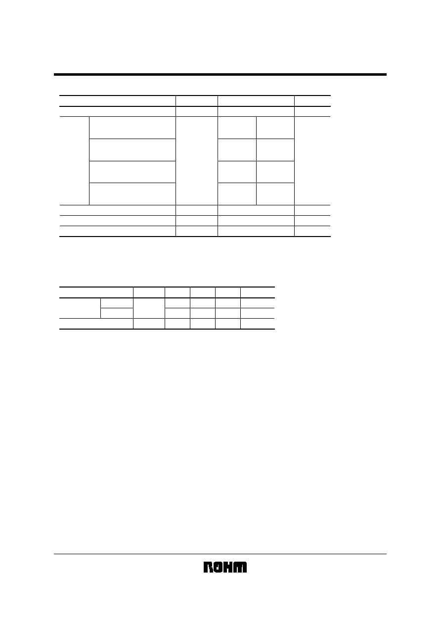
Absolute Maximum Ratings (Ta
=
25
°
C)
Parameter
Symbol
Limits
Unit
-
0.3
+
7.0
V
mW
800
1
450
2
300
3
DIP8
SSOP-B8
SOP8
MSOP8
310
4
-
65
+
125
°
C
-
40
+
85
°
C
V
CC
Pd
Tstg
Topr
-
-
0.3
V
CC
+
0.3
V
1 Degradation is done at 8.0mW/
°C for operation above Ta=25°C
2 Degradation is done at 4.5mW/
°C for operation above Ta=25°C
3 Degradation is done at 3.0mW/
°C for operation above Ta=25°C
4 Degradation is done at 3.1mW/
°C for operation above Ta=25°C
Supply Voltage
Power
dissipation
Storage Temperature
Operating Temperature
Terminal Voltage
BR9010-W,
BR9020-W,
BR9040-W
BR9010F-W,
BR9020F-W,
BR9040F-W
BR9010FV-W, BR9010RFV-W,
BR9020FV-W, BR9020RFV-W,
BR9040FV-W, BR9040RFV-W
BR9010RFVM-W,
BR9020RFVM-W,
BR9040RFVM-W
Recommended Operating Condition (Ta
=
25
°
C)
Parameter
Symbol
Min.
Typ.
Max.
Unit
V
CC
-
5.5
V
2.0
2.7
-
5.5
V
V
IN
0
-
V
CC
V
Supply voltage
Write
Read
Input voltage
BR9010-W / F-W / FV-W / RFV-W / RFVM-W / BR9020-W / F-W / FV-W /
Memory IC
RFV-W / RFVM-W / BR9040-W / F-W / FV-W / RFV-W / RFVM-W
4/14
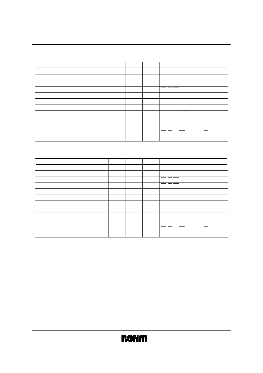
Electrical Characteristics
Unless otherwise specified ( Ta
=-
40~
+
85
°
C, V
CC
=
2.7V~5.5V)
Parameter
Min.
Typ.
Max.
Unit
Conditions
-
I
OL
=2.1mA
I
OH
=
-
0.4mA
DI pin
DI pin
CS, SK, WC pin
CS, SK, WC pin
V
IN
=0V
V
CC
-
-
-
-
-
-
-
-
-
-
-
-
Symbol
V
IL1
V
IH1
V
IL2
V
IH2
V
OL
V
OH
I
LI
I
LO
I
CC1
I
CC2
I
SB
f
SK
-
0.7
×
V
CC
-
0.8
×
V
CC
0
V
CC
-
0.4
-
1
-
1
-
-
-
-
V
V
V
V
V
V
µ
A
µ
A
mA
mA
µ
A
MHz
0.3
×
V
CC
-
0.2
×
V
CC
-
0.4
V
CC
2
1
3
2
1
1
V
OUT
=0V
V
CC
, CS=V
CC
CS, SK, DI, WC=V
CC
, DO, R / B=OPEN
f
SK
=2MHz, tE / W=10ms (WRITE)
f
SK
=2MHz (READ)
Input LOW Voltage 1
Input HIGH Voltage 1
Input LOW Voltage 2
Input HIGH Voltage 2
Output LOW Voltage
Output HIGH Voltage
Input Leakage Current
Output Leakage Current
Operating Current
Standby Current
Clock Frequency
Unless otherwise specified ( Ta
=-
40~
+
85
°
C, V
CC
=
2.7V~3.3V)
Parameter
Min.
Typ.
Max.
Unit
Conditions
-
I
OL
=100
µ
A
I
OH
=
-
100
µ
A
DI pin
DI pin
CS, SK, WC pin
CS, SK, WC pin
V
IN
=0V
V
CC
-
-
-
-
-
-
-
-
-
-
-
-
Symbol
V
IL1
V
IH1
V
IL2
V
IH2
V
OL
V
OH
I
LI
I
LO
I
CC1
I
CC2
I
SB
f
SK
-
0.7
×
V
CC
-
0.8
×
V
CC
0
V
CC
-
0.4
-
1
-
1
-
-
-
-
V
V
V
V
V
V
µ
A
µ
A
mA
mA
µ
A
MHz
0.3
×
V
CC
-
0.2
×
V
CC
-
0.4
V
CC
1.5
0.5
2
2
1
1
V
OUT
=0V
V
CC
, CS=V
CC
CS, SK, DI, WC=V
CC
, DO, R / B=OPEN
f
SK
=2MHz, tE / W=10ms (WRITE)
f
SK
=2MHz (READ)
Input LOW Voltage 1
Input HIGH Voltage 1
Input LOW Voltage 2
Input HIGH Voltage 2
Output LOW Voltage
Output HIGH Voltage
Input Leakage Current
Output Leakage Current
Operating Current
Standby Current
Clock Frequency
BR9010-W / F-W / FV-W / RFV-W / RFVM-W / BR9020-W / F-W / FV-W /
Memory IC
RFV-W / RFVM-W / BR9040-W / F-W / FV-W / RFV-W / RFVM-W
5/14
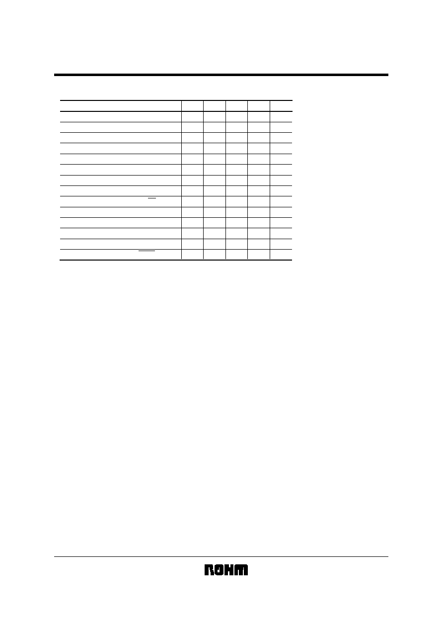
AC Operation Characteristics
( Ta
=-
40~
+
85
°
C, V
CC
=
2.7~5.5V)
Parameter
Symbol
Min.
Typ.
Max.
Unit
t
CSS
100
-
-
ns
t
CSH
100
-
-
ns
t
WCH
100
-
-
ns
t
DIS
100
-
-
ns
t
DIH
-
-
150
ns
t
PD1
-
-
150
ns
t
PD0
-
-
10
ms
t
E / W
250
-
-
ns
t
CS
-
-
150
ns
t
SV
0
-
150
ns
t
OH
230
-
-
ns
t
WH
230
-
-
ns
t
WL
0
-
-
ns
0
-
-
ns
t
WCS
Chip Select Setup Time
Clock High Time
Clock Low Time
Clock High to Output READY/BUSY Status
Data In Setup Time
Data In Hold Time
Delay to Output High
Delay to Output Low
Self-Timed Program Cycle
Minimum Chip Select High Time
Data Output Disable Time( From CS)
Chip Select Hold Time
Write Control Setup Time
Write Control Hold Time
BR9010-W / F-W / FV-W / RFV-W / RFVM-W / BR9020-W / F-W / FV-W /
Memory IC
RFV-W / RFVM-W / BR9040-W / F-W / FV-W / RFV-W / RFVM-W
6/14
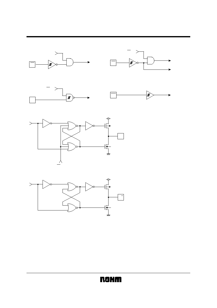
I / O Circuit
(1) Input Circuit
DI
CS int.
SK
CS int.
CS
RESET int.
WC
(2) Output Circuit
OE int.
DO
R/B
BR9010-W / F-W / FV-W / RFV-W / RFVM-W / BR9020-W / F-W / FV-W /
Memory IC
RFV-W / RFVM-W / BR9040-W / F-W / FV-W / RFV-W / RFVM-W
7/14
Operating
(1) Instruction Code
1010
1000
A0 A1 A2 A3 A4 A5 (
A6)
2
(A7)
1
A0 A1 A2 A3 A4 A5 (
A6)
2
(A7)
1
1010
0100
1010
0011
D0 D1
-
D14 D15 (READ DATA)
D0 D1
-
D14 D15 (WRITE DATA)
1010
0000
READ
WRITE
Write Enable (WEN)
Write Disable (WDS)
Address and data must be transferred from LSB.
BR9020-W/F-W/FV-W/RFV-W/RFVM-W
1
=
"0"
BR9010-W/F-W/FV-W/RFV-W/RFVM-W
1, 2
=
"0"
Instruction
Start Bit
Op Code
Address
Data
Means either V
IH
or V
IL
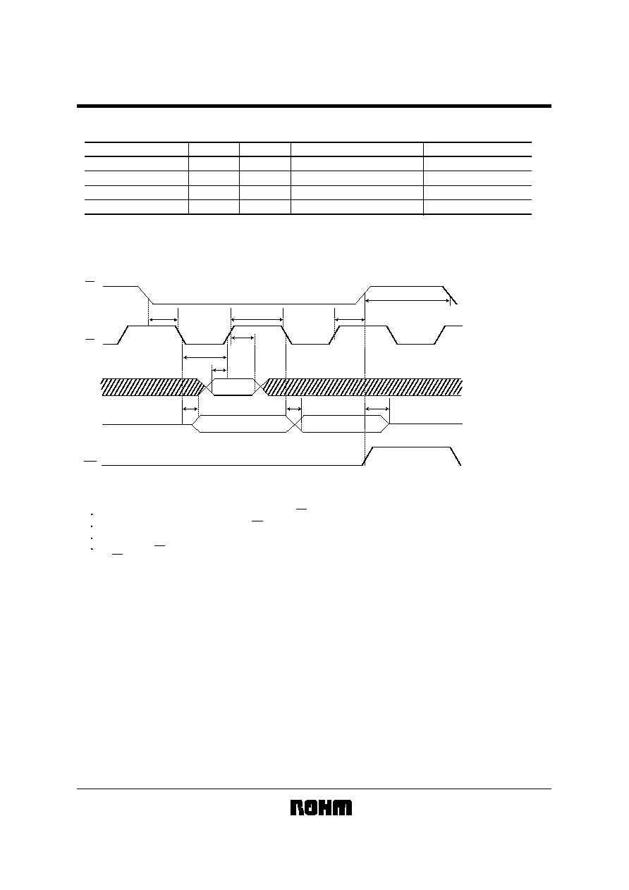
Synchronous Data Input Output Timing
CS
SK
DI
DO
WC
t
DIS
t
DIH
t
CSS
t
PD
t
OH
t
CSH
t
CS
t
PD
t
WL
t
WH
Input Data is clocked into the DI pin on the rising edge of the clock SK
Output data is clocked out on the falling edge of the SK clock.
The WC pin does not have any affect on the READ, WEN and WDS operations.
Between instructions, CS must be brought High for greater than the minimum of
t
CS
. If CS is maintained Low, the next instruction isn't detected.
Fig.1
BR9010-W / F-W / FV-W / RFV-W / RFVM-W / BR9020-W / F-W / FV-W /
Memory IC
RFV-W / RFVM-W / BR9040-W / F-W / FV-W / RFV-W / RFVM-W
8/14
(2) WRITE Enable / Disable
HIGH or LOW
Fig.2
1
1
High-Z
H
SK
CS
DI
DO
R / B
WC
L
H
L
H
L
H
0
1
0
0
0
4
8
ENABLE
=
11
DISABLE
=
00
12
16
1) When power is first applied, the device has been held in a reset status, with respect to the write enable, in the same
way the write disable (WDS) instruction is executed. Before the write instruction is executed, the device must be
received the write enable (WEN) instruction. Once the device is done, the device remains programmable until the
write disable (WDS) instruction is executed or the supply is removed from the device.
2) It is unnecessary to add the clock after 16
th clock. If the device is recieved the clock, the device ignores the clock.
3) As both of the enable and disable instructions don't depend on the status of the WC pin, the state of WC isn't cared
during the instruction.
4) The instruction is recognized after the rising edge of 8 th clock for the address following 8 clocks for the opcode, but
the specified address isn't cared during the instructions.
BR9010-W / F-W / FV-W / RFV-W / RFVM-W / BR9020-W / F-W / FV-W /
Memory IC
RFV-W / RFVM-W / BR9040-W / F-W / FV-W / RFV-W / RFVM-W
9/14
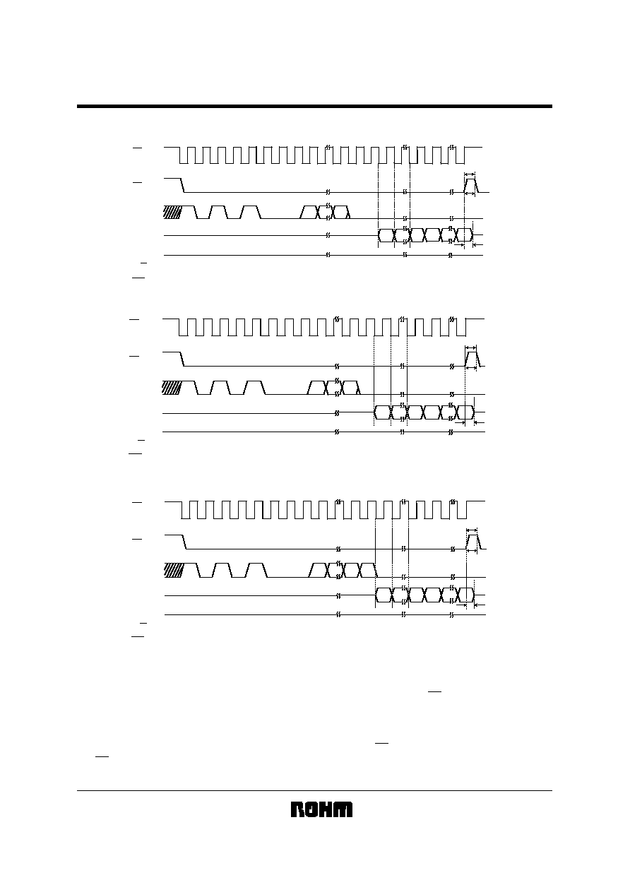
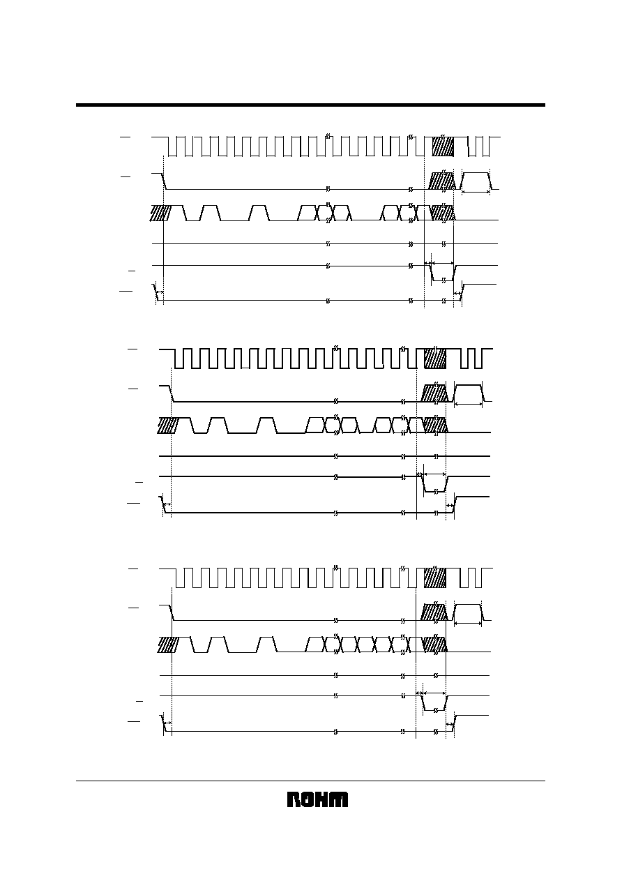
(3) Read Cycle
HIGH or LOW
Fig.3 BR9010-W / F--W / FV-W / RFV-W / RFVM-W
1
4
8
16
32
1
HIGH-Z
H
SK
CS
DI
DO
WC
L
H
L
H
L
0
1
1
0
0
0
0
A0
A5
0
0
D0
D15
D15
D0
HIGH-Z
STANDBY
t
CS
t
OH
R / B
H
Read Data (n)
Read Data (n+1)
HIGH or LOW
Fig.4 BR9020-W / F-W / FV-W / RFV-W / RFVM-W
1
4
8
16
32
48
1
HIGH-Z
H
SK
CS
DI
DO
R / B
WC
L
H
L
H
L
H
0
1
1
0
0
0
0
A0
A6
0
D0
Read Data (n)
Read Data (n+1)
D15
D15
D0
HIGH-Z
STANDBY
t
CS
t
OH
HIGH or LOW
Fig.5 BR9040-W / F-W / FV-W / RFV-W / RFVM-W
1
4
8
16
32
1
HIGH-Z
H
SK
CS
DI
DO
R / B
WC
L
H
L
H
L
H
0
1
1
0
0
0
0
A0
A6
A7
D0
Read Data (n)
Read Data (n+1)
D15
D15
D0
HIGH-Z
STANDBY
t
CS
t
OH
1) On the falling edge of 16 th clock, the data stored in the specified address (n) is clocked out of the DO pin.
The Output DO is toggled after the internal propagation t
PDO
or
t
PD1
on the falling edge of SK. During t
PD0
or t
PD1,
the data
is the previous data or unstable, and to take in the data, t
PD
is needed. (Refer to Fig.1 Synchronous data input output
timing.)
2) The data stored in the next address is clocked out of the device on the falling edge of 32nd clock. The data stored in
the upper address every 16 clocks is output sequentially by the continual SK input. Also the read operation is reset by
CS High.
BR9010-W / F-W / FV-W / RFV-W / RFVM-W / BR9020-W / F-W / FV-W /
Memory IC
RFV-W / RFVM-W / BR9040-W / F-W / FV-W / RFV-W / RFVM-W
10/14
(4) Write Cycle
Fig.6 BR9010-W / F-W / FV-W / RFV-W / RFVM-W
1
4
8
16
32
1
High-Z
High-Z
H
SK
CS
DI
DO
WC
L
H
L
H
L
H
L
0
1
0
0
1
0
0
0
0
A0
A5
D0
D15
t
WCH
t
WCS
t
CS
R / B
H
t
SV
t
E/W
Fig.7 BR9020-W / F-W / FV-W / RFV-W / RFVM-W
R / B
H
t
SV
1
4
8
16
32
1
High-Z
High-Z
H
SK
CS
DI
DO
WC
L
H
L
H
L
H
L
0
1
0
0
1
0
0
0
A0
A6
D0
D15
t
WCH
t
E/W
t
WCS
t
CS
Fig.8 BR9040-W / F-W / FV-W / RFV-W / RFVM-W
R / B
H
t
SV
1
4
8
16
32
1
High-Z
High-Z
H
SK
CS
DI
DO
WC
L
H
L
H
L
H
L
0
1
0
0
1
0
0
A0
A6
A7
D0
D15
t
WCH
t
E/W
t
WCS
t
CS
BR9010-W / F-W / FV-W / RFV-W / RFVM-W / BR9020-W / F-W / FV-W /
Memory IC
RFV-W / RFVM-W / BR9040-W / F-W / FV-W / RFV-W / RFVM-W
11/14
1) During the write instruction , CS must be brought Low. However once the write operation started, CS may be either
High or Low. But in the case of connecting the WC pin to the CS pin. CS and WC must be brought Low during
programming cycle.(If the WC pin is brought High during the write cycle, the write operation is halted. In that case, the
data of the specified address is not guaranteed. It is necessary to rewrite it.)
2) After the R / B pin changed Busy to Ready, once CS is brought High, then CS keep Low ,which means the status of
being able to accept an instruction. The device can take in the input from SK and DI, but in the case of keeping CS
Low without being brought High once, the input is canceled until being CS High once.
3) At the rising edge of 32 nd clock, the R / B pin will be driven Low after the specified time delay (tSV).
4) During programming, R / B is tied to Low by the device (On the rising edge of SK taken in the last data (D15), internal
timer starts and automatically finished after the data of memory cell is written spending tE / W. SK could be either High
or Low at the time.
5) After input write instruction, also the DO pin will be able to show the status of R / B, in the case that CS is falling from
High to Low while SK is tied to Low. (Refer to READY / BUSY STATUS in the next page.)
(5) READY / BUSY STATUS (on the R / B pin, the DO pin)
1)The DO pin outputs the READY / BUSY status of the internal part, which shows whether the device is ready to receive
the next instruction or not. (High or Low)
After the write instruction is completed, if CS is brought from high to low while SK is Low, the DO pin outputs the
internal status. (The R / B pin may be no connection.
2) When written to the memory cell, R / B status is output after tSV spent from the rising edge of 32 th clock on SK.
R / B =Low : under writing
After spending tE / W operating the internal timer, the device automatically finishes writing.
During tE / W, the memory array is accessed and any instruction is not received.
R / B=High : ready
Auto programming has been completed. The device is ready to receive the next Instruction.
Fig.9 R / B Status Output Timing
SK
CS
DI
DO
READY
READY
READY
BUSY
t
PD
t
OH
BUSY
WRITE INSTRUCTION
CLOCK
R / B
HIGH-Z
HIGH-Z

BR9010-W / F-W / FV-W / RFV-W / RFVM-W / BR9020-W / F-W / FV-W /
Memory IC
RFV-W / RFVM-W / BR9040-W / F-W / FV-W / RFV-W / RFVM-W
12/14
(6) About the direct connection between the DI and DO pins
The device can be used with the DI pin connected to the DO pin directly.
But when the READY / BUSY status is output, be careful about the bus conflict on the port of the controller.
Attention to Use
(1) Power ON / OFF
1) The CS is brought High during powerup and powerdown.
2) This device is in active state while CS is Low.
3) The extraordinary function or data collapse may occur in that condition because of noise etc, if powerup and power
down is done with CS brought Low.
In order to prevent above errors from happening, keep CS High during power-up and power-down.
(Good example) CS is brought High during powerup and power-down.
Please take more than 10ms between powerup and power-off, or the internal circuit is not always
reset.
(Bad example) CS is brought Low during powerup and power-down.
The CS pin is always Low in this case, the noise may force the device to make malfunction or
inadvertent write.
It sometimes occurs in the case that the CS pin is Hi-Z.
V
CC
V
CC
GND
V
CC
GND
CS
Good
Bad
Fig.10
(2) Noise Rejection
1) SK NOISE
If SK line has a lot of noise for rising time of SK, the device may recognize the noise as a clock and then clock will be
shifted.
2) WC NOISE
If WC line has noise during write cycle (tE / W), there may be a chance to deny the programming.
3) VCC NOISE
It recommended that capacitor is put between VCC and GND to prevent these case, since it is possible to occur
malfunction by the effect of noise or surge on power line.
BR9010-W / F-W / FV-W / RFV-W / RFVM-W / BR9020-W / F-W / FV-W /
Memory IC
RFV-W / RFVM-W / BR9040-W / F-W / FV-W / RFV-W / RFVM-W
13/14
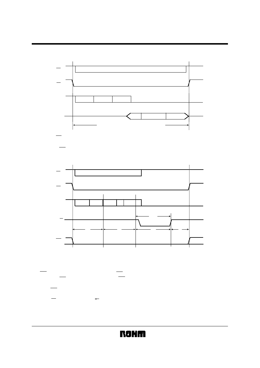
(3) Instruction Mode Cancel
1) Read instruction
32 clocks
START BIT
4 bit
4 bit
8 bit
16 bit
It is possible to be canceled for any timing.
DATA
DO
D15
OPCODE
ADDRESS
SK
CS
DI
DO
WC
HIGH or LOW
Fig.11
How to cancel : CS is brought High.
2) Write instruction
32 clocks
START BIT
4 bit
c
4 bit
8 bit
16 bit
DO
D15
OPECODE
ADDRESS
DATA
SK
CS
DI
R / B
WC
t
E / W
d
b
a
Fig.12
How to cancel
a
CS is brought High to cancel the instruction, and WC may be either High or Low.
b
In case that WC is brought High for a moment, or CS is brought High, the write instruction is canceled, the data of the
specified address is not changed.
c
When WC is brought High, or the device is powered down (But the latter way is not recommended), the instruction is
canceled but the specified data is not guaranteed. Send the instruction again.
d
When CS is brought High during R/B High, the device is reset and ready to receive a next instruction.
NOTE : The document may be strategic technical data subject to COCOM regulations.
BR9010-W / F-W / FV-W / RFV-W / RFVM-W / BR9020-W / F-W / FV-W /
Memory IC
RFV-W / RFVM-W / BR9040-W / F-W / FV-W / RFV-W / RFVM-W
14/14
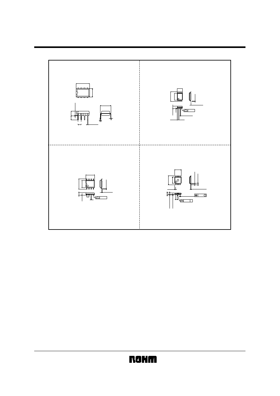
External dimensions (Units : mm)
DIP8
SSOP-B8
MSOP8
SOP8
5
4
8
1
0.1
6.4
±
0.3
4.4
±
0.2
3.0
±
0.2
0.22
±
0.1
1.15
±
0.1
0.65
(0.52)
0.15
±
0.1
0.3Min.
0.1
0.3Min.
0.15
±
0.1
0.4
±
0.1
0.11
6.2
±
0.3
4.4
±
0.2
5.0
±
0.2
8
5
4
1
1.27
1.5
±
0.1
0.1
4
1
5
8
2.9
±
0.1
0.475
0.65
4.0
±
0.2
0.6
±
0.2
0.29
±
0.15
2.
8
±
0.
1
0.75
±
0.05
0.08
±
0.05
0.9Max.
0.08 S
0.08
M
0.145
+
0.05
-
0.03
0.22
+
0.05
-
0.04
0.5
±
0.1
3.2
±
0.2
3.4
±
0.3
8
5
1
4
9.3
±
0.3
6.5
±
0.3
0.3
±
0.1
0.51Min.
2.54
0
°
~ 15
°
7.62
BR9010-W, BR9020-W, BR9040-W
BR9010F-W, BR9020F-W, BR9040F-W
BR9010FV-W, BR9010RFV-W
BR9020FV-W, BR9020RFV-W
BR9040FV-W, BR9040RFV-W
BR9010RFVM-W, BR9020RFVM-W, BR9040RFVM-W
Document Outline