 | –≠–ª–µ–∫—Ç—Ä–æ–Ω–Ω—ã–π –∫–æ–º–ø–æ–Ω–µ–Ω—Ç: BR9020F | –°–∫–∞—á–∞—Ç—å:  PDF PDF  ZIP ZIP |

1
Memory ICs
1, 2, and 4k bit EEPROMs for direct
connection to serial ports
BR9010 / BR9010F / BR9010FV / BR9020 /
BR9020F / BR9040 / BR9040F
∑
Overview
The BR90 series are serial EEPROMs that can be connected directly to a serial port and can be erased and written
electrically. Writing and reading is performed in word units, using four types of operation commands. Communication
occurs through CS, SK, DI, and DO pins, WC pin control is used to initiate a write disabled state, enabling these
EEPROMs to be used as one-time ROMs. During writing, operation is checked via the internal status check.
∑
Features
∑ BR9010 / F / FV (1k bit): 64 words
◊
16 bits
BR9020 / F (2k bit): 128 words
◊
16 bits
BR9040 / F (4k bit): 256 words
◊
16 bits
∑ Single power supply operation
∑ Serial data input and output
∑ Automatic erase-before-write
∑ Low current consumption
≠1.5mA (max.) active current: 3V
≠2
µ
A (max.) standby current: 3V
∑ Noise filter built into SK pin
∑ Compact DIP8, SOP8, SSOP-B8 packages (SSOP-
B8 is available only with BR9010).
∑ 100,000 ERASE / WRITE cycles
∑ 10 years Data Retention
∑ Easily connects to serial port
∑
Pin assignments
1
2
3
4
8
7
6
5
CS
SK
DI
DO
V
CC
R / B
WC
GND
BR9010 /
BR9020 / 9040
1
2
3
4
8
7
6
5
R / B
V
CC
CS
SK
WC
GND
DO
DI
BR9010F /
BR9010FV /
BR9020F /
BR9040F
∑
Pin description
CS
SK
DI
DO
GND
WC
V
CC
R / B
Function
Chip select input
Serial data clock input
Operating code, address, and serial data input
Serial data output
Reference voltage for all I / O, 0V
Write control input
READY, BUSY status signal output
Power supply connection
Pin
name
This pin is N.C. (non connection) on BR9010.
2
Memory ICs
BR9010 / BR9010F / BR9010FV / BR9020 / BR9020F /
BR9040 / BR9040F
∑
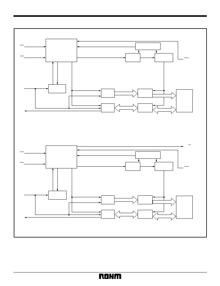
Block diagram
Command decode
Control
Clock generation
High voltage
generator
Write
disable
Address
buffer
Data
register
Command
register
Address
decoder
R / W
amplifier
1024bit
EEPROM
array
16bit
16bit
6bit
CS
SK
DI
DO
WC
6bit
Power supply
voltage detector
7 (8)
bit
2,048
(4,096) bit
EEPROM
array
16bit
16bit
7 (8)
bit
CS
SK
DI
DO
WC
R / B
Values in parentheses are for the BR9040 / F.
Command decode
Control
Clock generation
Power supply
voltage detector
Write
disable
High voltage
generator
Address
decoder
R / W
amplifier
Address
buffer
Data
register
Command
register
BR9010 / F / FV
BR9020 / F, BR9040 / F
3
Memory ICs
BR9010 / BR9010F / BR9010FV / BR9020 / BR9020F /
BR9040 / BR9040F
∑
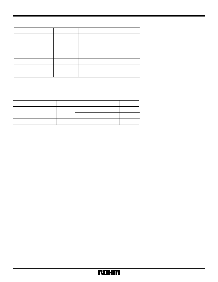
Absolute maximum ratings (Ta = 25∞C)
Parameter
Symbol
Limits
Unit
Applied voltage
Power dissipation
Storage temperature
Operation temperature
Input voltage
V
CC
P
d
T
stg
T
opr
--
≠ 0.3 ~ + 7.0
≠ 65 ~ + 125
≠ 40 ~ + 85
V
mW
∞
C
∞
C
V
Reduced by 5.0mw
1
/ 3.5mw
2
/ 3.0mw
3
for each increase in Ta of 1
∞
C over 25
∞
C.
DIP8
SOP8
SSOP-B8
500
1
350
2
300
3
≠ 0.3 ~ V
CC
+ 0.3
∑
Recommended operating conditions
Parameter
Symbol
Unit
Limits
Power supply voltage
Input voltage
V
CC
V
IN
2.7 to 5.5 (write)
2.0 to 5.5 (read)
0 ~ V
CC
V
V
V

4
Memory ICs
BR9010 / BR9010F / BR9010FV / BR9020 / BR9020F /
BR9040 / BR9040F
∑
Electrical characteristics
BR9010 / F / FV: At 5V (unless otherwise noted, Ta = ≠ 40 to + 85∞C, V
CC
= 5V ± 10%)
Parameter
Symbol
Min.
Typ.
Max.
Unit
Conditions
Input low level voltage 1
Input high level voltage 1
Input low level voltage 2
Input high level voltage 2
Output low level voltage
Output high level voltage
Input leak current
Output leak current
Consumption current
during operation
Standby current
SK frequency
V
IL1
V
IH1
V
IL2
V
IH2
V
OL
V
OH
I
LI
I
LO
I
CC1
I
CC2
I
SB
f
SK
--
0.7
◊
V
CC
--
0.8
◊
V
CC
0
V
CC
≠
0.4
--
--
--
--
--
--
--
--
--
--
--
--
--
--
--
--
0.3
◊
V
CC
--
0.2
◊
V
CC
--
0.4
V
CC
1
1
2
1
3
1
V
V
V
V
V
V
µ
A
µ
A
mA
mA
µ
A
MHz
DI Pin
DI Pin
CS, SK, WC Pin
CS, SK, WC Pin
I
OL
= 2.1mA
I
OH
= ≠ 0.4mA
V
IN
= 0V ~ V
CC
V
OUT
= 0V ~ V
CC
CS = V
CC
f = 1MHz tE / W = 10ms (WRITE)
f = 1MHz (READ)
CS, SK, DI, WC, = V
CC
DO = OPEN
≠ 1
≠ 1
--
BR9010 / F / FV: At 3V (unless otherwise noted, Ta = ≠ 40 to + 85∞C, V
CC
= 3V ± 10%)
Parameter
Symbol
Min.
Typ.
Max.
Unit
Conditions
Input low level voltage 1
Input high level voltage 1
Input low level voltage 2
Input high level voltage 2
Output low level voltage
Output high level voltage
Input leak current
Output leak current
Standby current
SK frequency
V
IL1
V
IH1
V
IL2
V
IH2
V
OL
V
OH
I
LI
I
LO
I
CC1
I
CC2
I
SB
f
SK
--
0.7
◊
V
CC
--
0.8
◊
V
CC
0
V
CC
≠
0.4
--
--
--
--
--
--
--
--
--
--
--
--
--
--
--
--
0.3
◊
V
CC
--
0.2
◊
V
CC
--
0.4
V
CC
1
1
1.5
500
2
1
V
V
V
V
V
V
µ
A
µ
A
mA
µ
A
µ
A
MHz
DI Pin
DI Pin
CS, SK, WC Pin
CS, SK, WC Pin
I
OL
= 100
µ
A
I
OH
= ≠ 100
µ
A
V
IN
= 0 ~ V
CC
V
OUT
= 0 ~ V
CC
CS = V
CC
f = 1MHz tE / W = 15ms (WRITE)
f = 1MHz (READ)
CS, SK, DI, WC, = V
CC
DO = OPEN
Not designed for radiation resistance
≠1
≠1
--
Consumption current
during operation

5
Memory ICs
BR9010 / BR9010F / BR9010FV / BR9020 / BR9020F /
BR9040 / BR9040F
∑
Electrical characteristics
∑
BR9020 / F: At 5V (unless otherwise noted, Ta = ≠ 40 to + 85∞C, V
CC
= 5V ± 10%)
Parameter
Symbol
Min.
Typ.
Max.
Unit
Conditions
Input low level voltage 1
Input high level voltage 1
Input low level voltage 2
Input high level voltage 2
Output low level voltage
Output high level voltage
Input leak current
Output leak current
Standby current
SK frequency
V
IL1
V
IH1
V
IL2
V
IH2
V
OL
V
OH
I
LI
I
LO
I
CC1
I
CC2
I
SB
f
SK
--
0.7
◊
V
CC
--
0.8
◊
V
CC
0
V
CC
≠ 0.4
--
--
--
--
--
--
--
--
--
--
--
--
--
--
--
--
0.3
◊
V
CC
--
0.2
◊
V
CC
--
0.4
V
CC
1
1
2
1
3
1
V
V
V
V
V
V
µ
A
µ
A
mA
mA
µ
A
MHz
DI Pin
DI Pin
CS, SK, WC Pin
CS, SK, WC Pin
I
OL
= 2.1mA
I
OH
= ≠ 0.4mA
V
IN
= 0V ~ V
CC
V
OUT
= 0V ~ V
CC
CS = V
CC
f
SK
= 1MHz tE / W = 10ms (WRITE)
f
SK
= 1MHz (READ)
CS, SK, DI, WC, = V
CC
DO, R / B = OPEN
--
≠ 1
≠ 1
Consumption current
during operation
∑
BR9020 / F: At 3V (unless otherwise noted, Ta = ≠ 40 to + 85∞C, V
CC
= 3V ± 10%)
Parameter
Symbol
Min.
Typ.
Max.
Unit
Conditions
Input low level voltage 1
Input high level voltage 1
Input low level voltage 2
Input high level voltage 2
Output low level voltage
Output high level voltage
Input leak current
Output leak current
Standby current
SK frequency
V
IL1
V
IH1
V
IL2
V
IH2
V
OL
V
OH
I
LI
I
LO
I
CC1
I
CC2
I
SB
f
SK
--
0.7
◊
V
CC
--
0.8
◊
V
CC
0
V
CC
≠ 0.4
--
--
--
--
--
--
--
--
--
--
--
--
--
--
--
--
0.3
◊
V
CC
--
0.2
◊
V
CC
--
0.4
V
CC
1
1
1.5
500
2
1
V
V
V
V
V
V
µ
A
µ
A
mA
µ
A
µ
A
MHz
DI Pin
DI Pin
CS, SK, WC Pin
CS, SK, WC Pin
I
OL
= 100
µ
A
I
OH
= ≠ 100
µ
A
V
IN
= 0V ~ V
CC
V
OUT
= 0V ~ V
CC
CS = V
CC
f
SK
= 1MHz tE / W = 15ms (WRITE)
f
SK
= 1MHz (READ)
CS, SK, DI, WC, = V
CC
DO, R / B = OPEN
--
≠ 1
≠ 1
Consumption current
during operation