Äîêóìåíòàöèÿ è îïèñàíèÿ www.docs.chipfind.ru

BR9080AF-W / BR9080ARFV-W / BR9080ARFVM-W /
Memory ICs
BR9016AF-W / BR9016ARFV-W / BR9016ARFVM-W
1/12
8k, 16k bit EEPROMs for direct
connection to serial ports
BR9080AF-W / BR9080ARFV-W / BR9080ARFVM-W /
BR9016AF-W / BR9016ARFV-W / BR9016ARFVM-W
The BR9080A and BR9016A series are serial EEPROMs that can be connected directly to a serial port and can be
erased and written electrically. Writing and reading is performed in word units, using four types of operation commands.
Communication occurs though CS, SK, DI, and DO pins, WC pin control is used to initiate a write disabled state, enabling
these EEPROMs to be used as one-time ROMs. During writing, operation is checked via the internal status check.
!
Applications
Movie, camera, cordless telephones, car stereos, VCRs, TVs, DIP switches, and other battery-powered equipment
requiring low voltage and low current
!
Features
1) BR9080AF-W / ARFV-W / ARFVM-W (8k bit) : 512 words
×16 bits
BR9016AF-W / ARFV-W / ARFVM-W (16k bit) : 1024 words
× 16bits
2) Single power supply operation
3) Serial data input and output
4) Automatic erase-before-write
5) Low current consumption
Active (5V) : 5mA (max.)
Standby (5V) : 3
µA (max.)
6) Noise filter built into SK pin
7) Write protection when V
CC
is low
Inhibition on inadvertant write with the WC pin.
8) SOP8 / SSOP-B8 / MSOP8
9) High reliability CMOS process
10) 100,000 ERASE / WRITE cycles
11) 10 years Data Retention
BR9080AF-W / BR9080ARFV-W / BR9080ARFVM-W /
Memory ICs
BR9016AF-W / BR9016ARFV-W / BR9016ARFVM-W
2/12
!
!
!
!
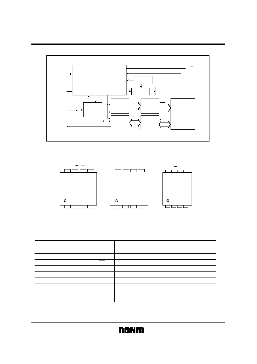
Block diagram
16bit
16bit
9bit
8,192 bit
EEPROM
CS
R / B
WC
SK
DI
DO
9bit
INSTRUCTION DECODE
CONTROL
CLOCK GENERATION
WRITE
DISABLE
DETECT
SUPPLY
VOLTAGE
HIGH
VOLTAGE
GENERATOR
ADD
DECORDER
R / W
AMPS
ADD
BUFFER
INSTRACTION
REGISTER
DATA
REGISTER
BR9016A is 10bit, 16,384bit
BR9080A is 9bit, 8,192bit
!
!
!
!
Pin descriptions
Fig.1
CS
SK
R / B
V
CC
WC
GND
DO
DI
BR9080ARFVM
BR9016ARFVM
: MSOP8
BR9080ARFV
BR9016ARFV
: SSOP-B8
BR9080AF
BR9016AF
: SOP8
CS
SK
DI
DO
V
CC
R / B
WC
GND
CS
SK
DI
DO
V
CC
R / B WC GND
3
4
5
6
7
8
1
2
1
2
3
4
5
6
7
8
CS
SK
DI
DO
GND
WC
R / B
V
CC
MSOP / SSOP
SOP
Pin No.
Pin name
Chip Select Control
Serial Data Clock Input
Op code, address, Serial Data Input
Ground 0V
Write Control Input
READY / BUSY Output
Power supply
Serial Data Output
Function
BR9080AF-W / BR9080ARFV-W / BR9080ARFVM-W /
Memory ICs
BR9016AF-W / BR9016ARFV-W / BR9016ARFVM-W
3/12
!
!
!
!
Absolute maximum ratings (Ta=25
°C)
Parameter
Symbol
Limits
Unit
-
0.3
+
7.0
V
mW
SOP8
SSOP-B8
450
1
300
2
MSOP8
310
3
-
65
+
125
°
C
-
40
+
85
°
C
V
CC
Pd
Tstg
Topr
-
-
0.3
V
CC
+
0.3
V
1 Reduced by 4.5mW for each increase in Ta of 1
°
C over 25
°
C.
2 Reduced by 3.0mW for each increase in Ta of 1
°
C over 25
°
C.
3 Reduced by 3.1mW for each increase in Ta of 1
°
C over 25
°
C.
Supply voltage
Power dissipation
Storage temperature
Operation temperature
Input voltage
!
!
!
!
Recommended operating conditions (Ta=25
°C)
Parameter
Symbol
Min.
Typ.
Max.
Unit
V
CC
-
5.5
V
2.7
2.7
-
5.5
V
V
IN
0
-
V
CC
V
Power supply voltage
WRITE
READ
Input voltage
BR9080AF-W / BR9080ARFV-W / BR9080ARFVM-W /
Memory ICs
BR9016AF-W / BR9016ARFV-W / BR9016ARFVM-W
4/12
!
!
!
!
Electrical characteristics
BR9080AF-W / ARFV-W / ARFVM-W, BR9016AF-W / ARFV-W / ARFVM-W : 5V
(Unless otherwise noted, Ta=
-4085°C, V
CC
=2.7V
5.5V)
Parameter
Symbol
Min.
Typ.
Max.
Unit
Conditions
V
IL1
-
-
0.3
×
V
CC
V
IH1
V
IL2
V
IH2
0.7
×
V
CC
-
0.8
×
V
CC
-
-
-
-
0.2
×
V
CC
-
-
V
OL
0
-
0.4
I
OL
=2.1mA
V
OH
V
CC
-
0.4
-
V
CC
I
OH
=
-
0.4mA
DI pin
DI pin
CS, SK, WC pin
CS, SK, WC pin
I
LI
-
1
-
V
IN
=0V
V
CC
I
LO
-
1
-
-
-
-
-
I
CC1
-
5
I
CC2
-
3
I
SB
f
SK
-
-
3
2
V
V
V
V
V
V
µ
A
µ
A
mA
mA
µ
A
MHz
1
1
V
OUT
=0V
V
CC
, CS=V
CC
CS / SK / DI / WC=V
CC
DO, R / B=OPEN
f
SK
=2MHz tE / W=10ms (WRITE)
f
SK
=2MHz (READ)
Input low level voltage 1
Input high level voltage 1
Input low level voltage 2
Input high level voltage 2
Output low level voltage
Output high level voltage
Input leak current
Output leak current
Operating current
Standby current
SK frequency
BR9080AF-W / ARFV-W / ARFVM-W, BR9016AF-W / ARFV-W / ARFVM-W : 3V
(Unless otherwise noted, Ta=
-4085°C, V
CC
=2.7V
3.3V)
Parameter
Symbol
Min.
Typ.
Max.
Unit
Conditions
V
IL1
-
-
0.3
×
V
CC
V
IH1
V
IL2
V
IH2
0.7
×
V
CC
-
0.8
×
V
CC
-
-
-
-
0.2
×
V
CC
-
-
V
OL
0
-
0.4
I
OL
=100
µ
A
V
OH
V
CC
-
0.4
-
V
CC
I
OH
=
-
100
µ
A
DI pin
DI pin
CS, SK, WC pin
CS, SK, WC pin
I
LI
-
1
-
V
IN
=0V
V
CC
I
LO
-
1
-
-
-
-
-
I
CC1
-
3
I
CC2
-
0.75
I
SB
f
SK
-
-
2
2
V
V
V
V
V
V
µ
A
µ
A
mA
mA
µ
A
MHz
1
1
V
OUT
=0V
V
CC
, CS=V
CC
CS / SK / DI / WC=V
CC
DO, R / B=OPEN
f
SK
=2MHz tE / W=10ms (WRITE)
f
SK
=2MHz (READ)
Input low level voltage 1
Input high level voltage 1
Input low level voltage 2
Input high level voltage 2
Output low level voltage
Output high level voltage
Input leak current
Output leak current
Operating current
Standby current
SK frequency
Not designed for radiation resistance
BR9080AF-W / BR9080ARFV-W / BR9080ARFVM-W /
Memory ICs
BR9016AF-W / BR9016ARFV-W / BR9016ARFVM-W
5/12
!
!
!
!
Operating timing characteristics
BR9080AF-W / ARFV-W / ARFVM-W, BR9016AF-W / ARFV-W / ARFVM-W
(Unless otherwise noted, Ta=
-4085°C, V
CC
=2.7V
5.5V)
Parameter
Symbol
Min.
Typ.
Max.
Unit
f
CSS
100
-
-
ns
t
CSH
100
-
-
ns
t
WCH
100
-
-
ns
t
DIS
100
-
-
ns
t
DIH
-
-
150
ns
t
PD1
-
-
150
ns
t
PD0
-
-
10
ms
t
E / W
250
-
-
ns
t
CS
-
-
150
ns
t
SV
0
-
150
ns
t
OH
230
-
-
ns
t
WH
230
-
-
ns
t
WL
0
-
-
ns
0
-
-
ns
t
WCS
CS setup time
Time when DO goes HIGH-Z (via CS)
Data clock high level time
Write control hold time
Data setup time
Data hold time
DO rise delay time
DO fall delay time
Self-timing programming cycle
CS minimum high level time
READY / BUSY display valid time
CS hold time
Data clock low level time
Write control setup time
!
!
!
!
Timing chart
Synchronous Data Input Output Timing
CS
SK
DI
DO
WC
t
DIS
t
DIH
t
CSS
t
PD
t
OH
t
CSH
t
CS
t
PD
t
WL
t
WH
· Input data are clocked in to DI at the rising edge of the clock (SK).
· Output data will toggle on the falling edge of the SK clock.
· The WC pin does not have any effect on the READ, EWEN and EWDS operations.
Fig.2
Document Outline