Äîêóìåíòàöèÿ è îïèñàíèÿ www.docs.chipfind.ru
1
Memory ICs
4,096-Bit Serial Electrically Erasable PROM
BR93LC66 / BR93LC66F / BR93LC66RF / BR93LC66FV
·
Features
· Low power CMOS Technology
· 256
×
16 bit configuration
· 2.7V to 5.5V operation
· Low power dissipation
3mA (max.) active current: 5V
5
µ
A (max.) standby current: 5V
· Auto increment for efficient data bump
· Automatic erase-before-write
· Hardware and software write protection
Default to write-disable state at power up
Software instructions for write-enable / disable
Vcc lockout inadvertent write protection
· 8-pin SOP / 8-pin SSOP-B / 8-pin DIP packages
· Device status signal during write cycle
· TTL compatible Input / Output
· 100,000 ERASE / write cycles
· 10 years Data Retention
·
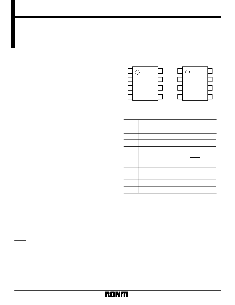
Pin assignments
·
Pin descriptions
1
2
3
4
8
7
6
5
CS
SK
DI
DO
V
CC
N.C.
N.C.
GND
BR93LC66 /
BR93LC66RF
1
2
3
4
8
7
6
5
NC
V
CC
CS
SK
N.C.
GND
DO
DI
BR93LC66F /
BR93LC66FV
CS
SK
DI
DO
GND
N.C.
N.C.
V
CC
Function
Chip select input
Serial clock input
Start bit, operating code, address, and serial
data input
Serial data output, READY / BUSY internal
status display output
Ground
Not connected
Not connected
Power supply
Pin
Name
·
Overview
The BR93LC66 series are CMOS serial input / output-type memory circuits (EEPROMs) that can be programmed
electrically. Each is configured of 256 words
×
16 bits (4096 bits), and each word can be accessed individually and
data read from it and written to it.
Operation control is performed using five types of commands. The commands, addresses, and data are input
through the DI pin under the control of the CS and SK pins. In a write operation, the internal status signal (READY or
BUSY) can be output from the DO pin.
2
Memory ICs
BR93LC66 / BR93LC66F / BR93LC66RF / BR93LC66FV
·
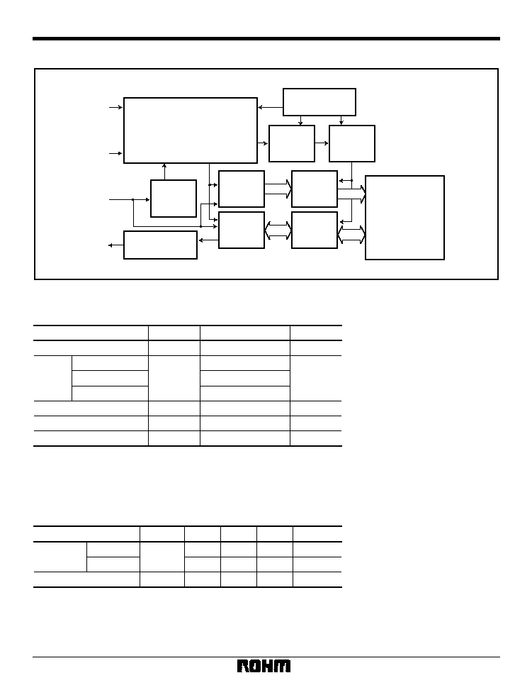
Block diagram
16bit
16bit
8bit
4096bit
EEPROM array
CS
SK
DI
DO
8bit
Command code
Control
Clock generation
Command
register
Dummy bit
Address
buffer
Data
register
Power supply
voltage detector
Write disable
High voltage
generator
Address
decoder
R / W
amplifier
·
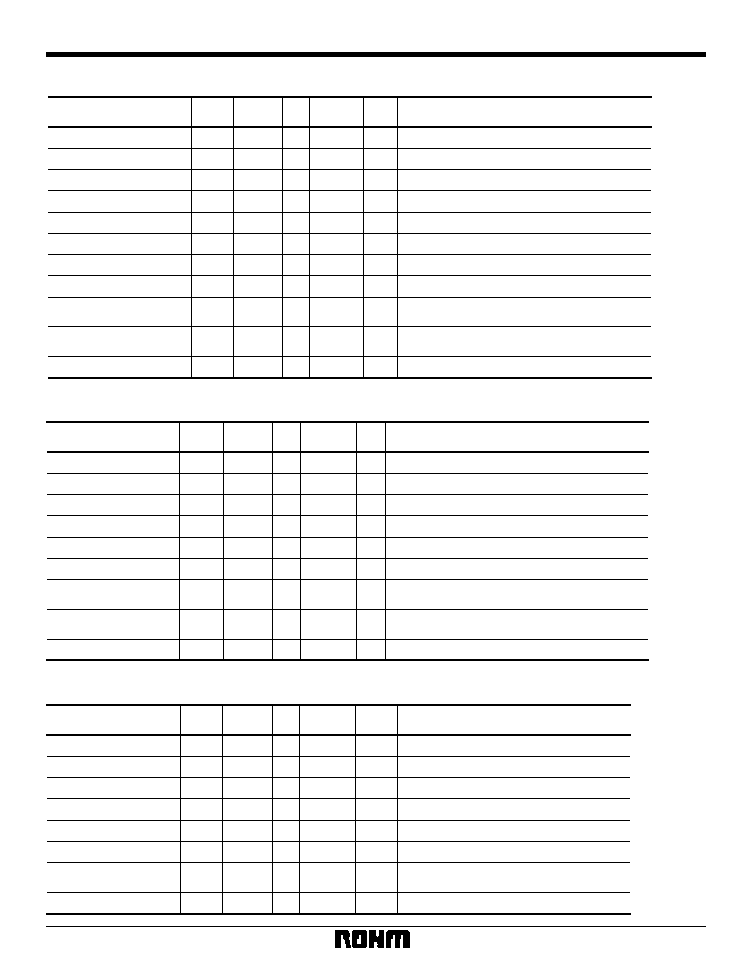
Absolute maximum ratings (Ta = 25°C)
Parameter
Symbol
Limits
Unit
V
CC
0.3 ~ + 6.5
V
BR93LC66
Pd
500
1
mW
BR93LC66F / RF
BR93LC66FV
350
2
300
3
Tstg
65 ~ + 125
°
C
Topr
40 ~ + 85
°
C
--
0.3 ~ V
CC
+ 0.3
V
Storage temperature
Operating temperature
Terminal voltage
1 Reduced by 5.0mW for each increase in Ta of 1
°
C over 25
°
C.
2 Reduced by 3.5mW for each increase in Ta of 1
°
C over 25
°
C.
3 Reduced by 3.0mW for each increase in Ta of 1
°
C over 25
°
C.
Applied voltage
Power
dissipation
·
Recommended operating conditions (Ta = 25°C)
Parameter
Symbol
Min.
Typ.
Max.
Unit
V
CC
--
5.5
V
2.0
--
5.5
V
V
IN
0
--
V
CC
V
2.7
Input voltage
Writing
Reading
Power supply
voltage
3
Memory ICs
BR93LC66 / BR93LC66F / BR93LC66RF / BR93LC66FV
·
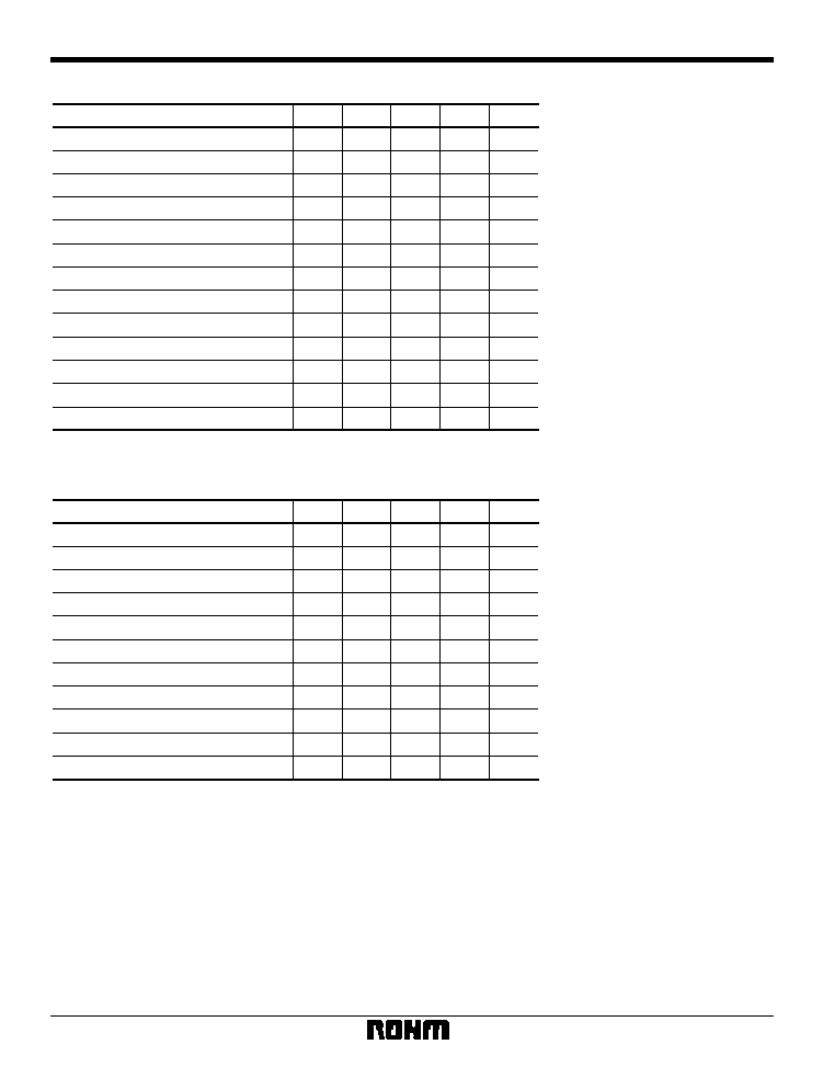
Electrical characteristics (unless otherwise noted, Ta = 40 to 85°C, V
CC
= 5V ± 10%)
Parameter
Symbol
Min.
Typ.
Max.
Unit
Conditions
V
IL
0.3
--
0.8
V
V
IH
2.0
--
--
--
V
CC
+ 0.3
V
V
OL1
--
--
0.4
V
I
OL
= 2.1mA
V
OH1
2.4
--
--
V
I
OH
= 0.4mA
V
OL2
--
--
0.2
V
I
OL
= 10
µ
A
V
OH2
V
CC
0.4 --
--
V
I
OH
= 10
µ
A
I
LI
1.0
--
µ
A
V
IN
= 0V ~ V
CC
I
LO
1.0
--
µ
A
I
CC1
--
1.5
3
mA
I
CC2
--
0.7
1.5
mA
I
SB
--
1.0
5
µ
A
1.0
1.0
V
OUT
= 0V ~ V
CC
, CS = GND
V
IN
= V
IH
/ V
IL
, DO = OPEN, fsk = 1MHz, WRITE
V
IN
= V
IH
/ V
IL
, DO = OPEN, fsk = 1MHz, READ
CS = SK = DI = GND, DO = OPEN
Input low level voltage
Input high level voltage
Output low level voltage 1
Output high level voltage 1
Output low level voltage 2
Output high level voltage 2
Input leakage current
Output leakage current
Standby current
Operating current
dissipation 1
Operating current
dissipation 2
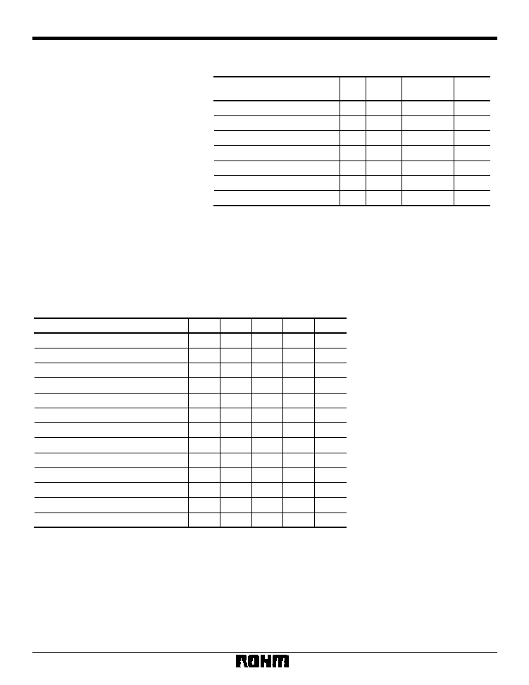
(unless otherwise noted, Ta = 40 to 85°C, V
CC
= 3V ± 10%)
Parameter
Symbol
Min.
Typ.
Max.
Unit
Conditions
V
IL
0.3
-- 0.15
×
V
CC
V
V
IH
0.7
×
V
CC
--
V
CC
+ 0.3
V
V
OL
--
--
0.2
V
I
OL
= 10
µ
A
V
OH
V
CC
0.4 --
--
V
I
OH
= 10
µ
A
I
LI
1.0
--
µ
A
V
IN
= 0V ~ V
CC
I
LO
1.0
--
µ
A
I
CC1
--
0.5
2
mA
I
CC2
--
0.2
1
mA
I
SB
--
0.4
3
µ
A
1.0
1.0
V
OUT
= 0V ~ V
CC
, CS = GND
CS = SK = DI = GND, DO = OPEN
V
IN
= V
IH
/ V
IL
, DO = OPEN, fsk = 250kHz, WRITE
V
IN
= V
IH
/ V
IL
, DO = OPEN, fsk = 250kHz, READ
Input low level voltage
Input high level voltage
Output low level voltage
Output high level voltage
Input leakage current
Output leakage current
Standby current
Operating current
dissipation 1
Operating current
dissipation 2
--
--
·
Electrical characteristics (unless otherwise noted, Ta = 40 to 85°C, V
CC
= 2.0V)
Parameter
Symbol
Min.
Typ.
Max.
Unit
Conditions
V
IL
0.3
-- 0.15
×
V
CC
V
V
IH
0.7
×
V
CC
-- V
CC
+ 0.3
V
V
OL
--
--
0.2
V
I
OL
= 10
µ
A
V
OH
V
CC
0.4 --
--
V
I
OH
= 10
µ
A
I
LI
1.0
--
1.0
µ
A
V
IN
= 0V ~ V
CC
I
LO
1.0
--
1.0
µ
A
I
CC2
--
0.2
1
mA
I
SB
--
0.4
3
µ
A
V
OUT
= 0V ~ V
CC
, CS = 0V
CS = SK = DI = 0V, DO = OPEN
V
IN
= V
IH
/ V
IL
, DO = OPEN, fsk = 200kHz,
READ
Input low level voltage
Input high level voltage
Output low level voltage
Output high level voltage
Input leakage current
Output leakage current
Operating current
dissipation 2
Standby current
--
--
4
Memory ICs
BR93LC66 / BR93LC66F / BR93LC66RF / BR93LC66FV
(2) Operation timing characteristics
(unless otherwise noted, Ta = 40 to 85°C, V
CC
= 5V ± 10%)
Parameter
Symbol
Min.
Typ.
Max.
Unit
f
SK
--
--
1
MHz
t
SKH
450
--
--
ns
t
SKL
450
--
--
ns
t
CS
450
--
--
ns
t
CSS
50
--
--
ns
t
DIS
100
--
--
ns
t
CSH
0
--
--
ns
t
DIH
100
--
--
ns
t
PD1
--
--
500
ns
t
PD0
--
--
500
ns
t
SV
--
--
500
ns
t
DF
--
--
100
ns
--
--
10
ms
t
E / W
SK clock frequency
SK "H" time
SK "L" time
CS "L" time
CS setup time
DI setup time
CS hold time
DI hold time
Data "1" output delay time
Data "0" output delay time
Time from CS to output confirmation
Time from CS to output High impedance
Write cycle time
·
Circuit operation
(1) Command mode
With these ICs, commands are not
recognized or acted upon until the
start bit is received. The start bit is
taken as the first "1" that is received
after the CS pin rises.
1 After setting of the read command
and input of the SK clock, data corre-
sponding to the specified address is
output, with data corresponding to up-
per addresses then output in se-
quence. (Auto increment function)
2 When the write or write all address-
es command is executed, all data in the selected memory cell is erased automatically, and the input data is written to
the cell.
3 These modes are optional modes. Please contact Rohm for information on operation timing.
1
10
A7 ~ A0
1
00
11XXXXXX
1
01
A7 ~ A0
D15 ~ D0
1
00
01XXXXXX D15 ~ D0
1
00
00XXXXXX
1
11
A7 ~ A0
1
00
10XXXXXX
Read (READ)
1
Write Enabled (WEN)
Write (WRITE)
2
Write to All Addresses (WRAL)
2
Write Disabled (WDS)
Erase (ERASE)
3
Chip Erase (ERAL)
3
Command
Start
bit
Operating
code
Address
Data
X: Either V
IH
or V
IL
--
--
--
--
--
5
Memory ICs
BR93LC66 / BR93LC66F / BR93LC66RF / BR93LC66FV
For low voltage operation (unless otherwise noted, Ta = 40 to 85°C, V
CC
= 3V ± 10%)
Parameter
Symbol
Min.
Typ.
Max.
Unit
f
SK
--
--
250
kHz
t
SKH
1
--
--
µ
s
t
SKL
1
--
--
µ
s
t
CS
1
--
--
µ
s
t
CSS
200
--
--
ns
t
DIS
400
--
--
ns
t
CSH
0
--
--
ns
t
DIH
400
--
--
ns
t
PD1
--
--
2
µ
s
t
PD0
--
--
2
µ
s
t
SV
--
--
2
µ
s
t
DF
--
--
400
ns
--
--
25
ms
t
E / W
SK clock frequency
SK "H" time
SK "L" time
CS "L" time
CS setup time
DI setup time
CS hold time
DI hold time
Data "1" output delay time
Data "0" output delay time
Time from CS to output confirmation
Time from CS to output High impedance
Write cycle time
When reading at low voltage (Unless otherwise noted, Ta = 40 to 85°C, V
CC
= 2.0V)
Parameter
Symbol
Min.
Typ.
Max.
Unit
f
SK
--
--
200
kHz
t
SKH
2
--
--
µ
s
t
SKL
2
--
--
µ
s
t
CS
2
--
--
µ
s
t
CSS
400
--
--
ns
t
DIS
800
--
--
ns
t
CSH
0
--
--
ns
t
DIH
800
--
--
ns
t
PD1
--
--
4
µ
s
t
PD0
--
--
4
µ
s
t
DF
--
--
800
ns
SK clock frequency
SK "H" time
SK "L" time
CS "L" time
CS setup time
DI setup time
CS hold time
DI hold time
Data "1" output delay time
Data "0" output delay time
Time from CS to output High impedance
Not designed for radiation resistance.