 | –≠–ª–µ–∫—Ç—Ä–æ–Ω–Ω—ã–π –∫–æ–º–ø–æ–Ω–µ–Ω—Ç: BU2090F | –°–∫–∞—á–∞—Ç—å:  PDF PDF  ZIP ZIP |

1
Standard ICs
BU2090 / BU2090F / BU2090FS /
BU2092 / BU2092F / BU2092FV
12-bit, serial IN, parallel OUT driver
BU2090 / BU2090F / BU2090FS /
BU2092 / BU2092F / BU2092FV
The BU2090, BU2090F, BU2090FS, BU2092, BU2092F, and BU2092FV are 12-bit serial input, parallel output
drivers.
For the BU2090 / F / FS, data input is shifted to the 12-bit internal shift register on the rising edge of a clock pulse.
On the falling edge of the pulse, if the DATA pin is HIGH, the data in the shift register is output in parallel to Q0 to
Q11.
For the BU2092 / F / FV, shift data read at the rising edge of CLOCK is output in parallel to Q0 to Q11 at the rising
edge of LCK. These ICs also have an OE pin, which when HIGH, forces data to be output, regardless of the shift
data state.
∑
Applications
Radio cassette players, telephones, compact audio systems, car stereos, and others
∑
Features
1) Low power dissipation.
2) Operating voltages ranging from 2.7 to 5.5V.
3) Output is Nch open drain.
4) High output withstand voltage of + 25V.
5) Diverse variety of packages.
BU2090 / F / FS: DIP16, SOP16, SSOP-A16
BU2092 / F / FV: DIP18, SOP18, SSOP-A18
(plastic molds)
6) High drive capability; direct lighting of green LED
possible.
2
Standard ICs
BU2090 / BU2090F / BU2090FS /
BU2092 / BU2092F / BU2092FV
∑
Absolute maximum ratings (Ta = 25∞C)
(BU2090 / F / FS, BU2092 / F / FV)
Parameter
Symbol
Limits
Unit
Power supply voltage
Power
dissipation
Power
dissipation
Operating temperature
Storage temperature
Input voltage
Output voltage
V
DD
≠ 0.3 ~ + 7.0
V
BU2090 / F / FS
Pd
1000 (DIP), 300 (SOP), 500 (SSOP)
1
1050 (DIP), 450 (SOP), 400 (SSOP)
1
mW
BU2092 / F / FV
BU2090 / F / FS
Pd
500 (SOP)
2
, 650 (SSOP)
3
500 (SOP)
2
, 650 (SSOP)
4
mW
BU2092 / F / FV
Topr
≠ 25 ~ + 75
∞
C
Tstg
≠ 55 ~ + 125
∞
C
V
IN
V
SS
≠ 0.3 ~ V
DD
+ 0.3
V
V
O
V
SS
~ 25.0
V
1 Unmounted
2 When mounted on a glass epoxy board of 50mm
◊
50mm
◊
1.6mm
3 When mounted on a glass epoxy board of 90mm
◊
50mm
◊
1.6mm
4 When mounted on a glass epoxy board of 70mm
◊
70mm
◊
1.6mm
∑
Recommended operating conditions
Parameter
Symbol
Limits
Unit
Power supply voltage
V
DD
2.7 ~ 5.5
V
3
Standard ICs
BU2090 / BU2090F / BU2090FS /
BU2092 / BU2092F / BU2092FV
∑
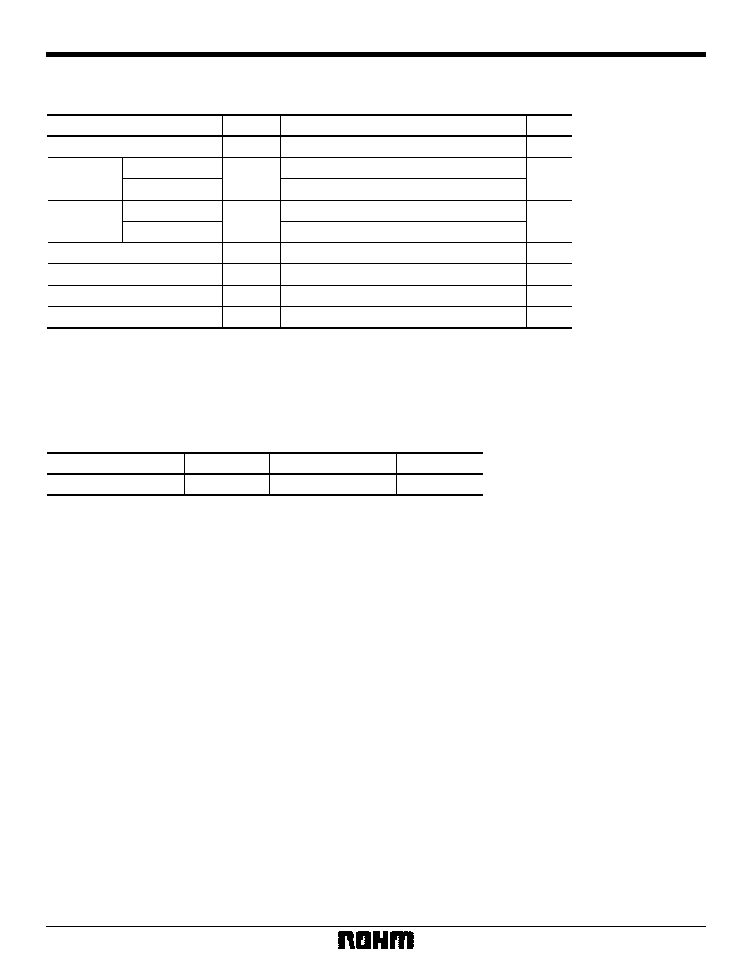
Block diagram
Control circuit
12-bit shift register
Latch
V
SS
2
1
3
4
5
6
7
8
DATA
CLOCK
Q0
Q1
Q2
Q3
Q4
16
15
14
13
12
11
10
9
V
DD
V
SS
2
1
3
DATA
CLOCK
Q0
Q1
Q2
Q3
Q4
V
DD
4
LCK
5
6
7
8
9
10
11
12
13
14
15
16
OE
17
18
Q11
Q10
Q9
Q8
Q7
Q6
Q5
Q11
Q10
Q9
Q8
Q7
Q6
Q5
Output buffer
(open drain)
BU2090 / F / FS
BU2092 / F
Control circuit
Output buffer
(open drain)
12-bit shift register
1
12-bit storage register
V
SS
2
1
3
DATA
CLOCK
Q0
Q1
Q2
Q3
Q4
V
DD
4
LCK
5
6
7
8
9
12
13
14
15
16
17
18
OE
19
20
Q11
Q10
Q9
Q8
Q7
N.C.
N.C.
BU2092FV
Control circuit
Output buffer (open drain)
12-bit shift register
12-bit storage register
Q5
10
11
Q6
4
Standard ICs
BU2090 / BU2090F / BU2090FS /
BU2092 / BU2092F / BU2092FV
∑
Pin descriptions
Pin name
1
1
GND
Serial data input
Data shift clock input
Data latch clock input
Parallel data output
Parallel data output
Parallel data output
Parallel data output
Parallel data output
Parallel data output
Parallel data output
Not connected
Not connected
Parallel data output
Parallel data output
Parallel data output
Parallel data output
Parallel data output
Output Enable
Power supply
2
2
DATA
3
3
CLOCK
--
4
LCK
4
5
Q0
5
6
Q1
6
7
Q2
7
8
Q3
8
9
Q4
9
10
Q5
10
11
Q6
N.C.
N.C.
--
--
Q7
--
--
Q8
11
12
Q9
12
13
Q10
13
14
Q11
14
15
OE
15
16
V
SS
V
DD
BU2090 / F / FS
BU2092 / F
1
2
3
4
5
6
7
8
9
10
11
12
13
14
15
16
17
18
--
17
19
16
18
20
BU2092 / FV
Pin No.
Function
5
Standard ICs
BU2090 / BU2090F / BU2090FS /
BU2092 / BU2092F / BU2092FV
∑
Electrical characteristics (Ta = 25∞C)
DC characteristics (unless otherwise noted, Ta = 25∞C, V
SS
= 0V)
Parameter
Symbol
Min.
Typ.
Max.
Unit
V
DD
Conditions
V
IH
3.5
--
--
V
5
2.5
--
--
--
--
3
V
IL
--
--
1.5
V
5
--
--
0.4
3
V
OL
--
--
2.0
V
5
I
OL
= 20mA
--
--
1.0
3
5
5
I
OL
= 5mA
I
OZH
--
--
10.0
µ
A
V
O
= 25.0V
I
OZL
--
--
≠ 5.0
µ
A
V
O
= 0V
I
DD
--
--
5.0
µ
A
5
V
IN
= V
SS
or V
DD
--
--
3.0
3
OUTPUT: OPEN
Input high level voltage
Input low level voltage
Output low level voltage
"H" output disable current
"L" output disable current
Current dissipation
BU2090 / F / FS switching characteristics (unless otherwise noted, Ta = 25∞C, V
SS
= 0V)
Parameter
Symbol
Min.
Typ.
Max.
Unit
V
DD
Conditions
Minimum clock pulse width
Data shift setup time
Data shift hold time
Data latch setup time
Data latch hold time
Data latch "L" setup time
Data latch "L" hold time
t
W
500
--
--
ns
5
3
1000
--
--
t
SU
200
--
--
--
--
--
--
--
--
--
ns
5
3
300
--
--
t
H
200
--
--
ns
5
3
400
--
--
t
LSUH
50
--
--
ns
5
3
100
--
--
t
LHH
250
--
--
ns
5
3
500
--
--
t
LSUL
200
--
--
ns
5
3
400
--
--
t
LHL
250
--
--
ns
5
3
500
--
--
Not designed for radiation resistance.
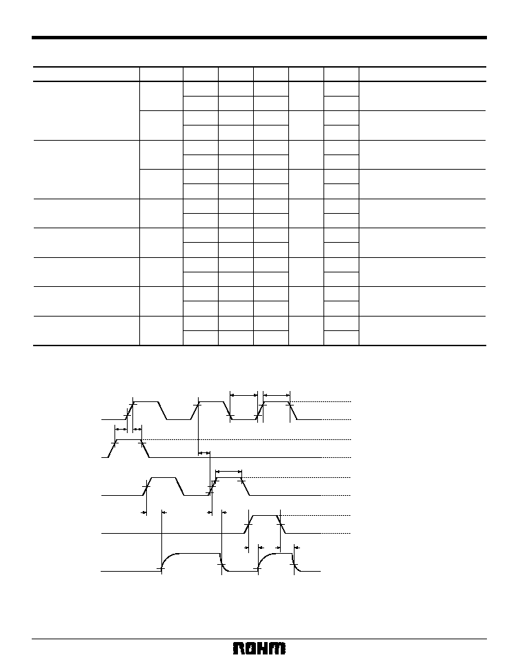
BU2090 / F / FS switching characteristics measurement conditions
90%
10%
90%
10%
10%
10%
10%
10%
90%
90%
90%
90%
90%
V
DD
V
DD
CLOCK
DATA
t
H
t
SU
t
LSUL
t
LHL
t
LHH
t
LSUH
t
W
t
W
GND (V
SS
)
GND (V
SS
)
Fig.1
6
Standard ICs
BU2090 / BU2090F / BU2090FS /
BU2092 / BU2092F / BU2092FV
BU2092 / F / FV switching characteristics (unless otherwise noted, Ta = 25∞C, V
SS
= 0V)
Parameter
Symbol
Min.
Typ.
Max.
Unit
V
DD
Conditions
Transmission delay time
(LCK to OUTPUT QX)
Output disable time
(OE to OUTPUT QX)
Minimum clock pulse width
Minimum latch pulse width
Setup time
(LCK to CLOCK)
Setup time
(DATA to CLOCK)
Hold time
(CLOCK to DATA)
--
55
--
ns
5
R
L
= 5k
C
L
= 10pF
--
90
--
3
--
50
--
ns
5
R
L
= 5k
C
L
= 10pF
--
115
--
3
t
PLZ
--
45
--
ns
5
R
L
= 5k
C
L
= 10pF
--
70
--
3
t
PZL
--
35
--
ns
5
R
L
= 5k
C
L
= 10pF
--
80
--
3
t
W
500
--
--
ns
5
1000
--
--
--
--
--
--
--
3
500
--
--
ns
5
1000
--
--
3
t
S
200
--
--
ns
5
400
--
--
3
t
SU
200
--
--
ns
5
400
--
--
3
t
H
200
--
--
ns
5
400
--
--
3
t
W (LCK)
t
PLZ (LCK)
t
PZL (LCK)
Not designed for radiation resistance.
BU2092 / F / FV switching characteristics measurement conditions
90%
10%
90% 90%
90%
10%
10%
90%
90%
50%
50%
90%
10%
90%
50%
50%
10%
50%
10%
50%
t
W
t
W
CLOCK
DATA
LCK
OE
Qx
V
DD
V
DD
V
DD
V
DD
t
SU
t
H
t
S
t
PLZ
t
PZL
t
W
(LCK)
GND (V
SS
)
GND (V
SS
)
GND (V
SS
)
GND (V
SS
)
t
PZL
(LCK)
t
PLZ
(LCK)
Fig.2
7
Standard ICs
BU2090 / BU2090F / BU2090FS /
BU2092 / BU2092F / BU2092FV
∑
Truth table
BU2092 / F / FV
INPUT
FUNCTION
CLOCK DATA
LCK
OE
◊
◊
◊
H
◊
◊
◊
L
L
◊
◊
H
◊
◊
◊
◊
◊
◊
◊
◊
◊
◊
◊
Output (Q0 to Q11) disabled
Output (Q0 to Q11) enabled
First cell of the shift register stores the LOW. Other cells, respectively, store
data from the preceding cells or other prior data. (Output state is HOLD.)
First cell of the shift register stores the HIGH. Other cells, respectively, store
data from the preceding cells or other prior data. (Storage state and output state are HOLD.)
No change in shift register.
Contents of shift register are stored in storage register.
No change in shift register.
Q0 to Q11 output for the BU2090 / F / FS and BU2092 / F / FV is Nch open drain output. When the shift register transfer data is LOW,
the corresponding output FET is ON (continuous state). When the transfer data is HIGH, the output FET is OFF (discontinuous).
∑
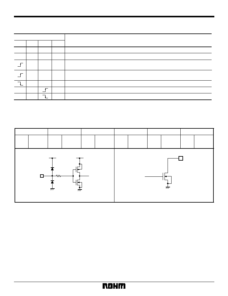
Input / output circuit
V
DD
V
DD
GND (V
SS
)
GND (V
SS
)
GND (V
SS
)
Pin No.
Pin No.
Pin No.
Pin No.
Pin No.
Pin No.
BU2090 / F / FS
BU2092 / F
BU2092FV
BU2090 / F / FS
BU2092 / F
BU2092FV
2, 3
2, 3, 4, 17
2, 3, 4, 19
10, 11, 12, 13
14, 15
4, 5, 6, 7, 8, 9
10, 11, 12, 13
14, 15, 16
5, 6, 7, 8, 9,
10, 11, 14, 15
16, 17, 18
5, 6, 7, 8, 9,
8
Standard ICs
BU2090 / BU2090F / BU2090FS /
BU2092 / BU2092F / BU2092FV
∑
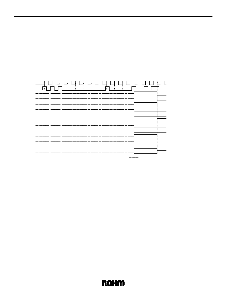
Circuit operation
The logic of the DATA pin is sent to the 12-bit shift register on the rising edge of the CLOCK pulse. Subsequently, it
is shifted from Q0 to Q11 for every clock rising edge.
For the BU2090 / F / FS
When the DATA pin is LOW on the CLOCK falling edge, the data does not change its output state. It is only shifted in
the internal shift register. However, when the DATA pin is HIGH, the content of the 12-bit shift register is latched and
is output to the corresponding Q0 to Q11.
D11
D10
D8
D7
D6
D5
D4
D3
D2
D1
D0
D9
CLOCK
DATA
Note 1) indicates unstable output.
Note 2) Pull-up resistance is connected to the output pin.
Q11
Q10
Q9
Q8
Q7
Q6
Q5
Q4
Q3
Q2
Q1
Q0
Fig.3 Operation timing chart
9
Standard ICs
BU2090 / BU2090F / BU2090FS /
BU2092 / BU2092F / BU2092FV
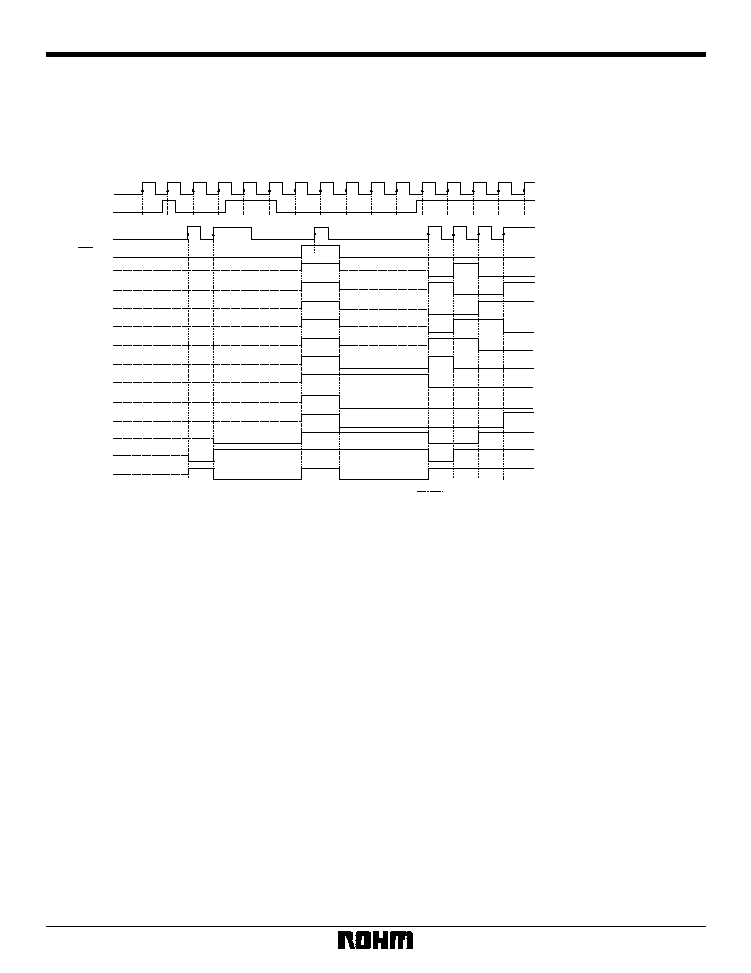
For the BU2092 / F / FV
The content of the 12-bit shift register is stored in the 12-bit storage register at the rising edge of LCK, and is output
to the corresponding Q0 to Q11. When OE is HIGH, regardless of the content of the storage register, the output FET
turns OFF and enters a HIGH (discontinuous) state.
LCK
OE
Q11
Q10
Q9
Q8
Q7
Q6
Q5
Q4
Q3
Q2
Q1
Q0
CLOCK
DATA
Note 1) indicates unstable output.
Note 2) Pull-up resistance is connected to the output pin.
D11
D10
D8
D7
D6
D5
D4
D3
D2
D1
D0
D9
Fig.4 Operation timing chart
10
Standard ICs
BU2090 / BU2090F / BU2090FS /
BU2092 / BU2092F / BU2092FV
∑
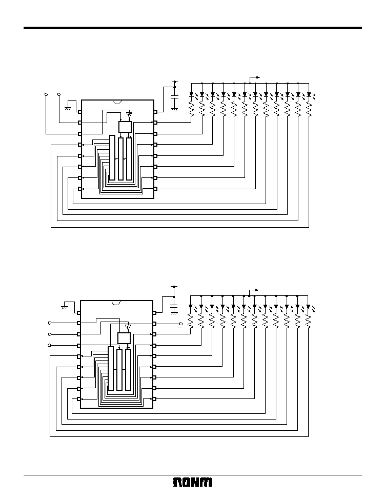
Application example
BU2090 / F / FS
Control
circuit
Output buffer (open drain)
12-bit shift register
LED power supply
GND
GND
Latch
V
DD
CLOCK DATA
(V
SS
)
(V
SS
)
Fig.5
BU2092 / F / (FV)
CLOCK
DATA
LED power supply
Control
circuit
Output buffer (open drain)
12-bit shift register
12-bit storage register
LCK
OE
GND
V
DD
GND (V
SS
)
(V
SS
)
Fig.6
11
Standard ICs
BU2090 / BU2090F / BU2090FS /
BU2092 / BU2092F / BU2092FV
∑
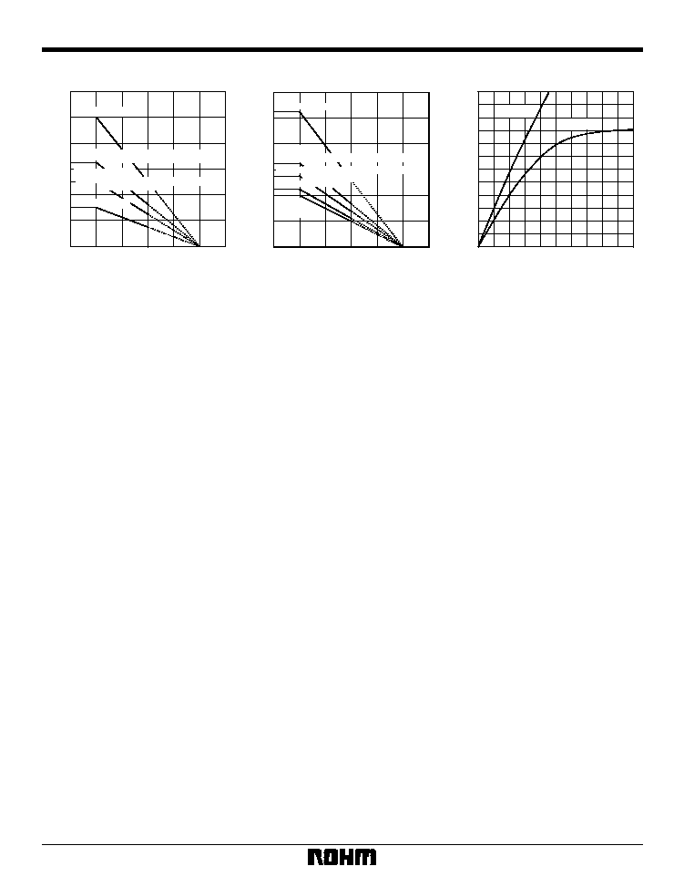
Electrical characteristic curves
25
50
75
100
125
150
0
SOP16
SSOP16 (Unmounted)
SSOP16
1200
1000
800
600
400
200
AMBIENT TEMPERATURE: Ta (
∞
C)
POWER DISSIPATION
: Pd (mW)
Fig.7 BU2090 / F / FS thermal derating
characteristics
DIP16 (Unmounted)
(when mounted on a 90mm
◊
50mm
◊
1.6mm
glass epoxy board)
(when mounted on a 50mm
◊
50mm
◊
1.6mm
glass epoxy board)
SOP16 (Unmounted)
25
50
75
100
125
0
200
400
600
800
1000
1200
150
DIP18 (Unmounted)
AMBIENT TEMPERATURE: Ta (
∞
C)
POWER DISSIPATION
: Pd (mW)
(When mounted on a 70mm
◊
70mm
◊
1.6mm glass epoxy board)
SSOP-B20
SSOP-B20
(Unmounted)
Fig.8 BU2092 / F / FV thermal derating
characteristics
(when mounted on a 50mm
◊
50mm
◊
1.6mm
glass epoxy board)
SOP18 (Unmounted)
SOP18
0.5
0
1.0
1.5
2.0
2.5
30
25
20
15
10
5
V
DD
=
5V
V
DD
=
3V
OUTPUT VOLTAGE "LOW" LEVEL: V
OL
(V)
OUTPUT CURRENT
"
LOW
"
LEVEL
:
I
OL
(
mA
)
Fig.9 Output current vs.output low level
voltage
12
Standard ICs
BU2090 / BU2090F / BU2090FS /
BU2092 / BU2092F / BU2092FV
∑
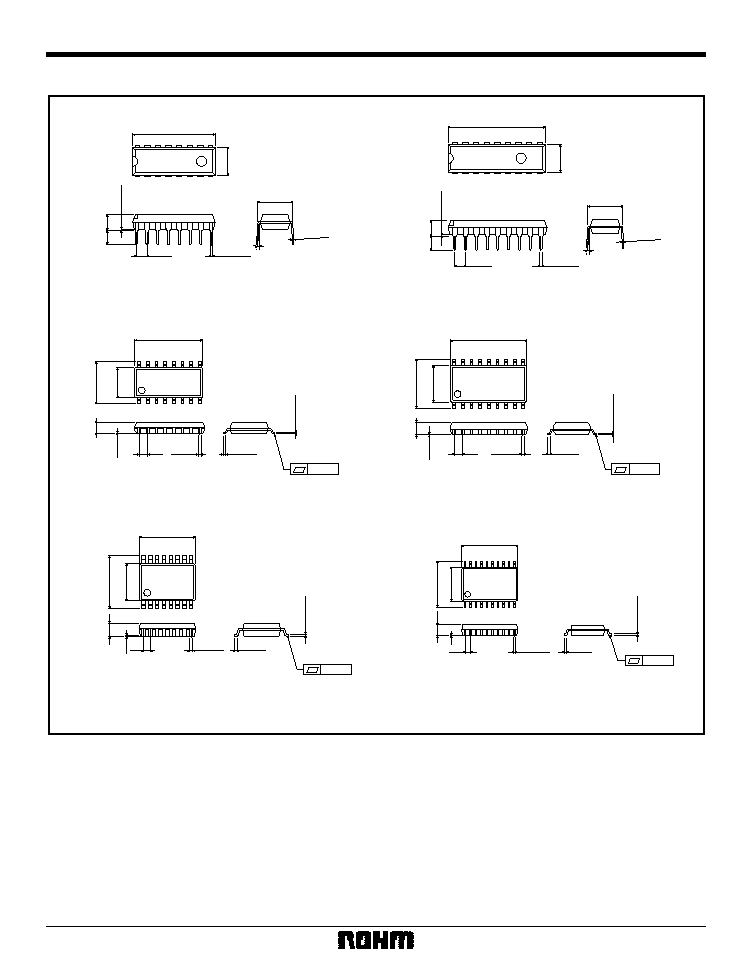
External dimensions (Units: mm)
DIP16
SOP16
DIP18
SOP18
BU2090F
BU2090FS
BU2092FV
BU2090
BU2092
BU2092F
0.51Min.
0.3
±
0.1
9
16
8
1
6.5
±
0.3
3.2
±
0.2
4.25
±
0.3
0.5
±
0.1
19.4
±
0.3
0.51Min.
18
10
9
1
6.5
±
0.3
22.9
±
0.3
3.29
±
0.2
0.5
±
0.1
0.3
±
0.1
2.54
0
∞
~ 15
∞
7.62
2.54
0
∞
~ 15
∞
7.62
SSOP-A16
SSOP-B20
0.4
±
0.1
1.27
0.15
0.15
±
0.1
0.3Min.
4.4
±
0.2
6.2
±
0.3
0.11
1.5
±
0.1
1
16
10.0
±
0.2
8
9
0.4
±
0.1
1.27
0.3Min.
0.11
1.8
±
0.1
5.4
±
0.2
7.8
±
0.3
0.15
±
0.1
18
1
11.2
±
0.2
10
9
0.15
0.36
±
0.1
0.8
0.11
6.6
±
0.2
4.4
±
0.2
6.2
±
0.3
1.5
±
0.1
1
16
8
9
0.15
0.3Min.
0.15
±
0.1
11
10
20
1
6.4
±
0.3
4.4
±
0.2
6.5
±
0.2
0.15
±
0.1
1.15
±
0.1
0.3Min.
0.1
11
10
20
1
0.1
6.4
±
0.3
4.4
±
0.2
6.5
±
0.2
0.15
±
0.1
0.22
±
0.1
0.65
1.15
±
0.1
0.3Min.
0.1