 | ÐлекÑÑоннÑй компоненÑ: BU2374FV | СкаÑаÑÑ:  PDF PDF  ZIP ZIP |
Äîêóìåíòàöèÿ è îïèñàíèÿ www.docs.chipfind.ru
BU2374FV
Multimedia ICs
1/7
VCO + phase comparator IC for PLL system
BU2374FV
BU2374FV is a VCO+phase comparator IC used to construct PLL system. PLL system is constructed and low
jitter clocks can be generated by adopting external LPF and divider. Through a mechanism incorporated in this
IC the output could be switched into quarter. Another function can set in the center point of frequency by
adjusting external resistance.
!
!
!
!
Applications
TV
!
!
!
!
Features
1) V
DD
=3.3V
±5% operating guaranteed
2) Oscillating range of VCO is 37MHz~60MHz
3) High-speed edge trigger type phase comparator
4) VCO can be fine-adjusted by external resistor.
5) VCO and phase comparator can be controlled
independently.
6) Small SSOP-B14 package
!
!
!
!
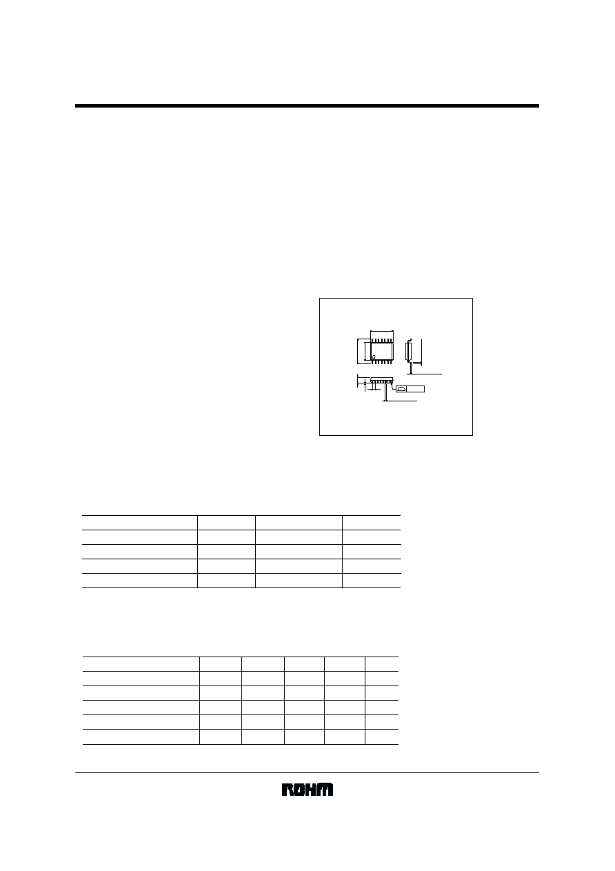
External dimensions (Unit : mm)
SSOP-B14
8
7
14
1
0.1
6.4 ± 0.3
4.4 ± 0.2
5.0 ± 0.2
0.22 ± 0.1
1.15 ± 0.1
0.65
0.15 ± 0.1
0.3Min.
0.1
!
!
!
!
Absolute maximum ratings (Ta=25
°C)
Parameter
Unit
V
V
°
C
Symbol
V
DD
V
IN
Tstg
Pd
Limits
-
0.5 to
+
7.0
-
0.5 to V
DD
+
0.5
-
30 to
+
125
400
mW
Applied voltalge
Inpuit voltage
Storage temperature
Power dissipation
An operation is not guaranteed.
In case it is used at Ta=25
°
C or more, 4.0mW is reduceed at every 1
°
C.
Radiation resistance design is not used.
Power dissipation is measured when BU2374FV is placed on the board.
!
!
!
!
Recommended operating conditions(Ta=25
°C)
Parameter
Symbol
Typ.
Max.
Unit
Supply voltage
V
DD
-
3.45
V
Input H voltage range
-
V
DD
V
IH
V
Input L voltage range
-
0.2V
DD
V
V
IL
Operating temperature
-
+
75
°
C
Topr
Output load
-
15
C
L
pF
Min.
3.15
0.8V
DD
0
-
20
-
BU2374FV
Multimedia ICs
2/7
!
!
!
!
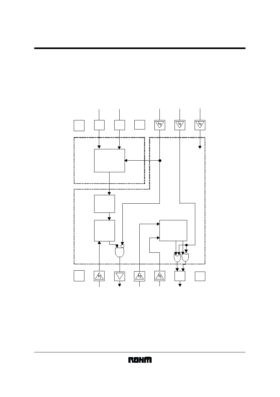
Block diagram
Through
or 1/4
Level
Shifter
Logic
V
DD
Phase
Detector
Logic
GND
VCO
V
DD
VCO
GND
Bias resistor
T
e
r
minal
(Connect a resistor betw
een
vco
V
DD
)
VCO frequency Control input
(F
orce DC
V
oltage)
VCO P
o
w
erdo
wn and Output
disab
le
(H :
disab
le L :
enab
le)
Phase Detector Output-Enab
le
(H :
disab
le L :
enab
le)
T
est Pin
(Nor
mally L or Open)
Pmos Gate
Nmos Gate
VCO
divide select
VCO Output
Frequency
Input 1
Frequency
Input 2
Phase Detect
Output
VCO
BU2374FV
Multimedia ICs
3/7
!
!
!
!
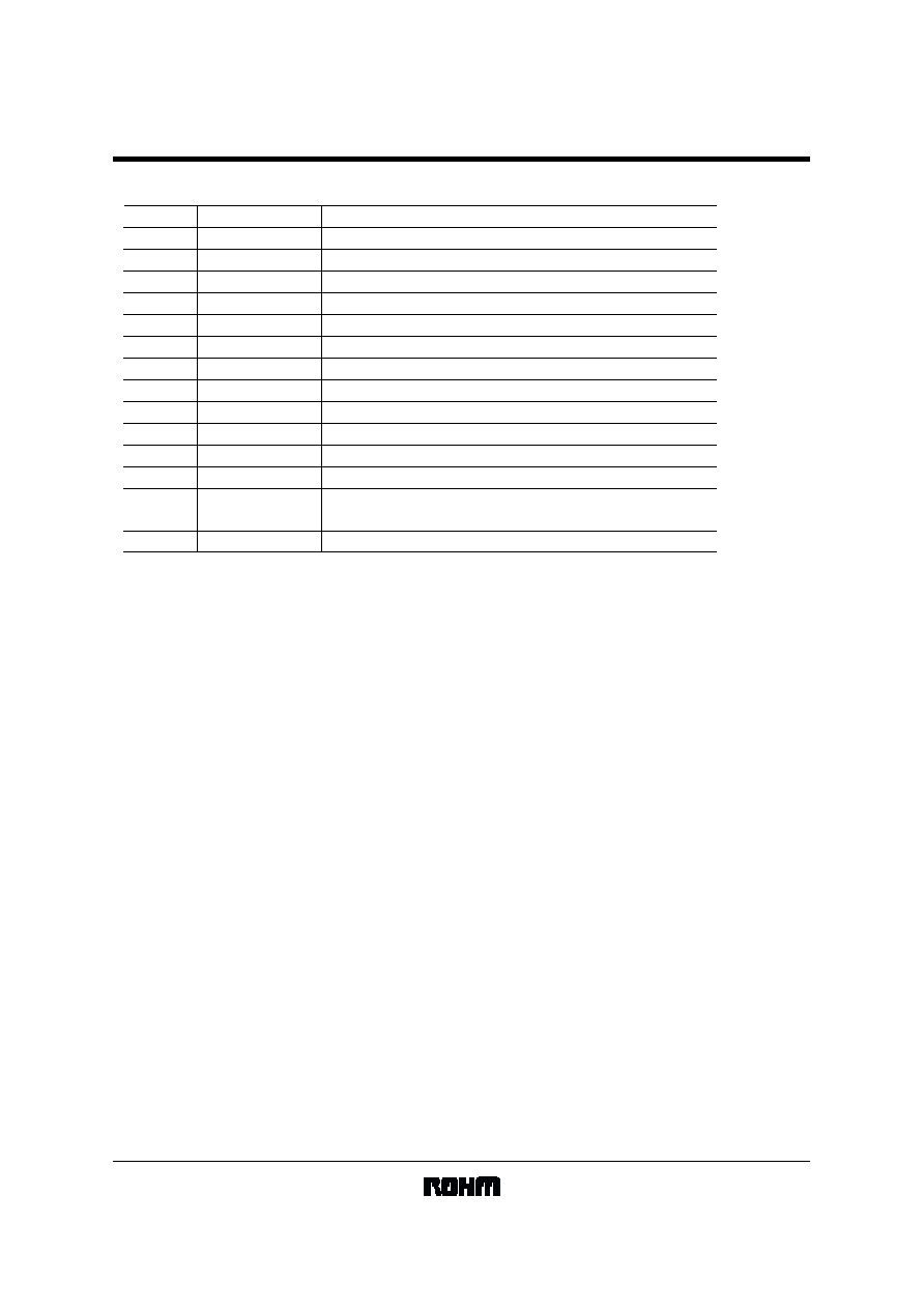
Pin descriptions
Functions
Pin No.
Pin name
1
Digital V
DD
2
VCO output frequency select (H:1/4 output, L:1/1 output)
4
Input reference frequency is applied to Fin A
6
PD output
7
Digital GND
5
Input for VCO external counter output frequency
VCO output
3
TEST input with Pull-down resistor (Normaly OPEN or 'L')
8
GND for VCO (Analog GND)
11
Contorol Pin for PD (H:PD disable (Hi impedance state), L:PD enable)
9
VCO control voltage input
12
V
DD
for VCO (Analog V
DD
)
14
For adjusting VCO output frequency range
(An external resistor connect between VCO_V
DD
and BIAS)
13
LOGIC V
DD
SELECT
FIN-A
PFD_OUT
LOGIC_GND
FIN-B
VCO OUT
TEST
VCO_GND
PFD_INHIBIT
VCO_IN
VCO_V
DD
BIAS
VCO_INHIBIT
VCO mode select (H:VCO OUT disable (L Fix), L:VCOOUT enable)
10
BU2374FV
Multimedia ICs
4/7
!
!
!
!
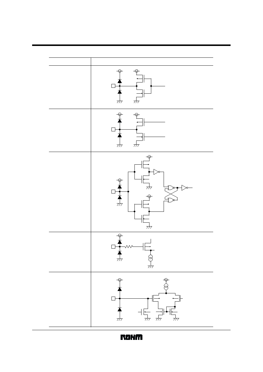
Input / output circuits
( Pin2, 4, 5, 8, 9, 10)
Pin8 : with pull-down
resistance
Input Pin (Schmitt triger)
(Pin3)
Output Pin
(Pin6)
Output Pin
(Pin12)
Input Pin
(Pin13)
Input Pin
From inside IC
From inside IC
From inside IC
To inside IC
Pin No.
Equivalent circuit
From inside IC
From inside IC
From inside IC
From inside IC
From inside IC
From inside IC
BU2374FV
Multimedia ICs
5/7
!
!
!
!
Electrical characteristics (Unless otherwise noted,Ta=25
°C, V
CC
=3.3V)
Conditions
I
OL
=
2.0mA
VCO_OUT Output L voltage
input current (VCO_INHIBIT, SELECT)
1
VCO section
VCO current consumption (inhibit)
at VCO_INHIBIT=V
DD
PFD_INHIBIT=V
DD
VCO frequency range
VCO control voltage
Bias Resistor range
1
1 Value of design
guarantee
(all guarantee range)
2 Frequency sersibility
3 When FSEL is H and output frequency is 1/4, culculate
Bias R
=
2.0k
37MHz to 54MHz
Bias R
=
2.4k
45MHz to 58MHz
Bias R
=
3.0k
53MHz to 60MHz
{ f1(VCOIN
=
2.0V)
-
f2(VCOIN
=
1.0V)} / 1.0V
I
OH
=-
2.0mA
VCO_OUT Output H voltage
input impedance (VCO_IN)
Output 50MHz
VCO current consumption (normal operation)
2
Frequency sersibility
at 1/2 V
DD
point
Output duty
Time is from V
DD
0.2 to vdd
0.8
Output Rise-time
Output Fall-time
Time is from V
DD
0.8 to vdd
0.2
Min.
-
-
-
37
0.5
2.0
3.0
-
-
-
45
-
-
Symbol
V
OL
IIH, IIL
I
DD
(INH)
frange
VI(vco_in)
Rbias
V
OH
Zi
I
DD
(vco)
1
Duty
tr
tf
Unit
V
µ
A
µ
A
MHz
V
K
V
M
mA
MHz/V
%
nsec
nsec
-
-
-
-
-
-
-
10
12.5
23
50
2.5
2.5
Typ.
Parameter
+
Max.
0.3
1
60
V
DD
-
0.5
3.0
-
-
-
-
55
-
-
-
Document Outline