 | ÐлекÑÑоннÑй компоненÑ: BU8732AKV | СкаÑаÑÑ:  PDF PDF  ZIP ZIP |
Äîêóìåíòàöèÿ è îïèñàíèÿ www.docs.chipfind.ru

BU8732AKV
Communication ICs
1/10
CODEC IC for digital mobile phone
BU8732AKV
BU8732AKV is a PCM codec IC for digital cellular phones. This includes plenty of analog input / output functions such as
a 14bit precision linear.
µ
/ A-LAW codec, a microphone amplifier with two systems, amplifiers for speaker and earphone
and a switch transistor for driving a ringer. This IC is the most suitable for both PDC system and CDMA system cellular
phones.
Application
Digital cellular phones with CDMA system, Digital cellular phones with PDC system.
Features
1) +3V single power supply. (V
DD
=2.7 to 3.3V)
2) 14bit precision linear
µ
/ A-LAW codec.
3) Transmission filter of the codec block is in conformity to the ITU-T recommendation G. 714.
4) Built-in PLL circuit for system clock generation.
5) Built-in DSP I/F which is in conformity with PDC and N-CDMA.
6) Arbitrary setting of the clock frequency of PCM data transmission is allowed :
µ
/ A-LAW
64kHz to 2048kHz
Linear 128kHz to 2048kHz
7) Plenty of input / output analog functions :
·
Two systems of built-in microphone amplifier (differential input type, single input type)
·
Built-in speaker amplifier for receiver (32
BTL type)
·
Built-in speaker amplifier for earphone (32
single type)
·
Built-in speaker amplifier for REXT of call receiving system (600
)
·
Built-in electronic volumes for gain adjustment. (Call-receiving system, call sending system, TONE system)
·
Built-in input / output circuit for data signal which allows external connection.
·
Pop noise of REXT earphone and receiver outputs at the time of switching on and off the power supply is reduced
by means of soft mute.
8) A built-in function to generate DTMF signals and musical scale tones is provided in the tone signal generating block.
9) Built-in switch transistor for driving a ringer.
10) VQFP 48 pin package.
BU8732AKV
Communication ICs
2/10
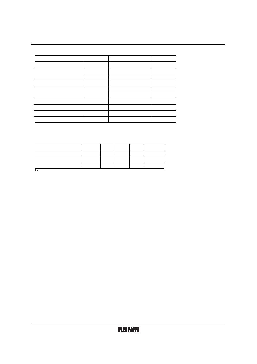
Absolute maximum rating (Ta=25
°
C unless specified particularly)
Parameter
Symbol
Limits
Unit
Digital power supply voltage
Analog power supply voltage
Digital pin apply voltage
Analog pin apply voltage
Input current
Power dissipation
Storage temperature range
Operation temperature range
DV
DD
RXV
DD
TXV
DD
V
TD
V
TA
I
IN
Pd
Tstg
Ta
-
0.3 to
+
4.5
-
0.3 to
+
4.5
-
0.3 to
+
4.5
DV
SS
-
0.3 to DV
DD
+
0.3
RXV
SS
-
0.3 to RXV
DD
+
0.3
TXV
SS
-
0.3 to TXV
DD
+
0.3
-
10 to
+
10
400
1
-
50 to
+
125
-
30 to
+
85
V
V
V
V
V
V
mA
mW
°
C
°
C
1 Drops by 4.0mW per 1
°
C when used at more than Ta=25
°
C.
Recommendable operation condition (Ta=25
°
C unless specified particularly)
Parameter
Symbol
Unit
Max.
Typ.
Min.
DV
DD
RXV
DD
TXV
DD
2.7
2.7
2.7
-
-
-
3.3
3.3
3.3
V
V
V
Digital power supply voltege
Analog power supply voltege
Radiation resistance is not included design.
BU8732AKV
Communication ICs
3/10
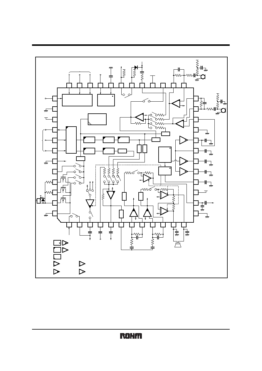
Block diagram
+-
+
-
36
35
34
33
32
31
30
29
28
27
26
25
12
11
10
9
8
7
6
5
4
3
2
1
37
38
39
40
41
42
43
44
45
46
47
48
13
14
15
16
17
18
19
20
21
22
23
24
CPU I / F
PLL
for CPU
DSP
8kHz
SW8
SW12
SW0
1
2
3
MIC
Amp2
MIC
Amp1
Amp1
Amp3
EAmp1
EAmp2
Amp5
Amp4
ERMT
SPMT
RAmp
JAmp
TEXT
R8
R7
C11
C10
C8
R5
MIC10
MIC1IP
TXV
SS
TXREF
REFC
CODECREF
RXREF
SMUTE
RXV
DD
RXV
SS
EARO
C7
EAR (32
)
SPC (32
)
1
µ
1
µ
1
µ
2.2
µ
0.22
µ
MIC1IN
C9
R6
frame syne
signal
reset
XPRSTB
PCMOUT
PCMIN
DCLK
CPUSEL
RGPULSE
RINGER1
RINGER
R9
R10
RINGER2
RINGER3
REXTDI
REXTDO
EXTO
RIN
AUDO
AUDVR
ERPN
ERPO
SPPN
SPPO
SPCOP
SPCON
PV
SS
(20
)
DV
SS
DV
DD
SDA
SRL
STB
FSYNC
PLLLPF
TEXTDO
TEXTDI
TEXTA
DD
TXV
DD
TAUDO
MIC20
MIC2IN
0.01
µ
DTMF / TONE
DSP I / F
PWM
RG0
EXTSEL
SW9A
REXT
Power on by
REFPON
Power on by
VCPON
Power on by
TGPON
Power on by
VCPON or TGPON
Power on by
RXPON
Power on by
SPCON
Power on by
EARON
R2
C2
R4
C4
C5
C6
C1
R1
C3
R3
SW4
5
6
7
SW9B
ERP0
SPP0
1
2
3
BPF
LPF
A / D
AAF
D / A
EV1
EV7
+
+
+
+
EV0
Vref /
COMMON
EV3
EV2
EV6
EV5
EV4
+
-
+
-
+
-
SOFTMUTE
+
+
+
+
+ -
+
-
+
-
+
-
+
+
+
+
+
+
+
+
+
BU8732AKV
Communication ICs
4/10
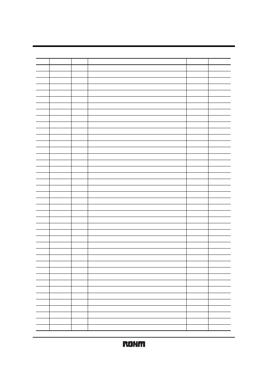
Pin descriptions
Pin No.
Pin name
Terminal function
1
2
3
4
5
6
7
8
9
10
11
12
13
14
15
16
17
18
19
20
21
22
23
24
25
26
27
28
29
30
31
32
33
34
35
36
37
38
39
40
41
42
REXTDI
REXTDO
EXTO
RIN
AUDO
AUDVR
ERPN
ERPO
SPPN
SPPO
SPCOP
SPCON
RXV
SS
EARO
RXV
DD
SMUTE
RXREF
CODCREF
REFC
TXREF
TXV
SS
MIC1IP
MIC1IN
MIC1O
MIC2IN
MIC2O
TAUDO
TXV
DD
TEXTADD
TEXTDI
TEXTDO
PLLLPF
FSYNC
STB
SCL
SDA
XPRSTB
DV
SS
DV
DD
PCMOUT
PCMIN
DCLK
I / O
I / O
I / O
O
I
O
O
I
O
I
O
O
O
-
O
-
I
O
O
O
O
-
I
I
O
I
O
O
-
I
I / O
I / O
I / O
I
I
I / O
I / O
I
-
-
O
I
I
-
-
-
-
50p
50p
-
50p
-
50p
-
-
-
-
-
0.22
µ
1
1
µ
1
1
µ
1
2.2
µ
1
1
µ
1
-
-
-
50p
-
50p
50p
-
-
-
-
0.01
µ
1
-
-
-
-
-
-
-
-
-
-
-
-
600
-
50k
50k
-
50k
-
50k
30(BTL)
30(BTL)
-
30
-
-
-
-
-
-
-
-
-
50k
-
50k
50k
-
-
-
-
-
-
-
-
-
-
-
-
-
-
-
Input of the data signal of receive
Output of the data signal of receive
Amplifier output for the gain adjustment of receive signal
Direct input of the voice of receive
Direct output of receive signal
External output of receive signal
Inverted amplifier input for the earphone gain adjustment
Amplifier output for the earphone gain adjustment
Inverted amplifier input for the speaker gain adjustment
Amplifier output for the speaker gain adjustment
Non-ineverted speaker amplifier output for the receiver
Inverted speaker amplifier output for the receiver
Analog grounding for the receive
Speaker amplifier output for the earphone
Analog power source for the receive
Time constant terminal for the soft mute setting
Analog reference voltage output for the receive
Analog reference voltage output for codec
Analog reference voltage output
Analog reference voltage output for the transmit
Analog grounding for the transmit
Non-inverted input of the microphone amplifier 1
Inverted input of the microphone amplifier 1
Output of microphone amplifier 1
Inverted input of the microphone amplifier 2
Output of microphone amplifier 2 output
External output of transmit signal
Analog power source for the transmit
Additive input of the transmit signal
Input of the data signal of transmit
Output of the data signal of transmit
Filter connection input/output for PLL
PLL reference clock input
Strobe input for CPU I/F
Shift clock input for CPU I/F
Address data input for CPU I/F
System reset input (L
:
reset)
Grounding for digital
Power supply for digital
Output of PCM signal
Input of PCM signal
Shift clock input for PCM signal
1 Standard value
Minimum load
resistance
[]
Maximum load
capacitance
[
F
]
BU8732AKV
Communication ICs
5/10
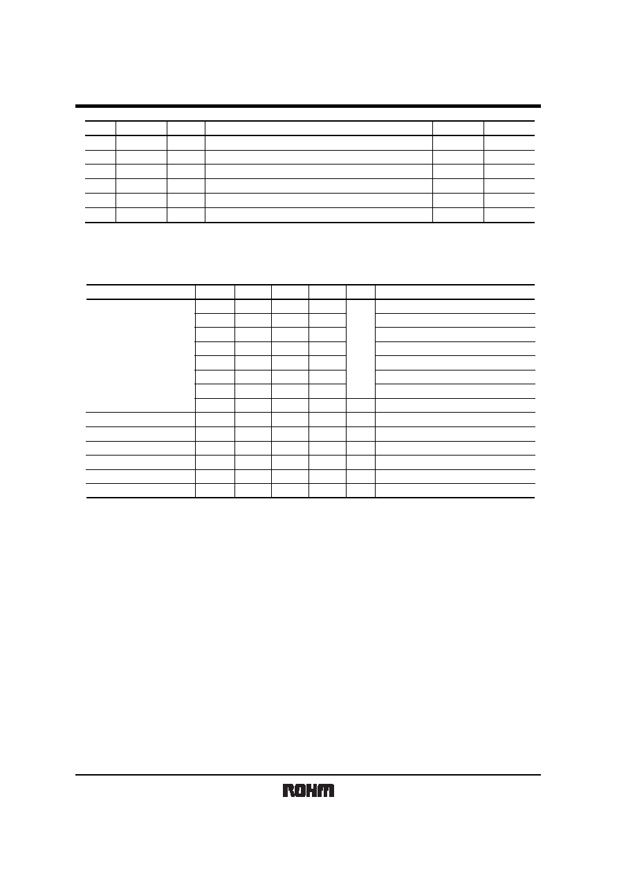
Pin No.
Pin name
Terminal function
43
44
45
46
47
48
CPUSEL
RGPULSE
RINGER1
RINGER2
RINGER3
PV
SS
I / O
I
O
O
O
O
-
-
-
-
-
-
-
-
-
100(at 3V)
60(at 3V)
20(at 3V)
-
Fixed to GND, Fixed "L"
Pulse output for the ringer
Open drain output of the ringer driving transistor
Open drain output of the ringer driving transistor
Open drain output of the ringer driving transistor
1 Standard value
Grounding for ringer
Minimum load
resistance
[]
Maximum load
capacitance
[
F
]
Electrical characteristics
(Ta=25
°
C, DV
DD
=RXV
DD
=TXV
DD
=3.0V, FSYNC=8kHz, gain 0dB unless specified particularly)
Parameter
Conditions
Current consumption
(
Note 1
)
Digital "H" level input voltage
Digital "L" level input voltage
Digital "H" level input current
Digital "L" level input current
Digital "H" level output voltage
Digital "L" level output voltage
Symbol
I
DD1
I
DD2
I
DD3
I
DD4
I
DD5
I
DD6
I
DD7
I
DD8
V
IH
V
IL
I
IH
I
IL
V
OH
V
OL
Min.
-
-
-
-
-
-
-
-
0.8DV
DD
-
-
-
10
DV
DD
-
0.5
-
Typ.
8.0
7.0
6.0
5.4
5.1
3.7
3.3
0.1
-
-
-
-
-
-
Max.
11.5
10.2
8.6
7.8
7.3
5.3
4.8
20
-
0.2DV
DD
10
-
-
0.5
Unit
mA
µ
A
V
V
µ
A
µ
A
V
V
Full operation
(
Note2
)
Reference / Voice / SPC ON
(
Note2
)
Reference / Voice / EAR ON
(
Note2
)
Reference / Voice / RAMP ON
(
Note2
)
Reference / Voice ON
(
Note2
)
Reference / Tone ON
(
Note2
)
Reference ON
(
Note2
)
All power down, FSYNC, Fixed DCLK terminal
V
IH
=
DV
DD
V
IL
=
0V
I
OH
= -
1mA
I
OL
=
1mA
1) Power
supply voltage (
DV
DD
, RXV
DD
, TXV
DD
) is 3V. Digital and analog output terminals are free from load.
All the digital terminals except FSYNC. CLK terminal are connected to either
DV
DD
or
DV
SS
.
Analog terminals are connected with an appropriate resistance to TXREF or RXREF.
The soft mute is in the canceled status. (SMUTE="0")
2)
FSYNC=8kHz, DCLK=256kHz
Document Outline