 | –≠–ª–µ–∫—Ç—Ä–æ–Ω–Ω—ã–π –∫–æ–º–ø–æ–Ω–µ–Ω—Ç: SA2531J | –°–∫–∞—á–∞—Ç—å:  PDF PDF  ZIP ZIP |

sames
SA2531 A/B/C/E/G/U
1/24
VERSATILE SINGLE CHIP TELEPHONE
WITH 14 NUMBER REPERTORY DIALLER
sames
SA2531 A/B/C/D/E/F/G/J/U
s
Speech circuit, LD/MF Repertory Dialler
and Tone Ringer on one 28 pin CMOS
chip
s
Net 4 compatible
s
Soft clip to avoid harsh distortion
s
Line Loss Compensation selectable by
pin option
s
Power down mode
s
Versatile applications for different PTT
demands
s
31 digit last number redial
s
Sliding Cursor protocol with comparison
s
2 Flash keys, 100 ms and 280 ms (option
600 ms)
s
Ring frequency discrimination
s
Operating range from 13 to 100 mA
(down to 5 mA with reduced perform-
ance)
s
Volume control of receive signalExcept
"D")
s
Low noise (max. -72dBmp)
s
Real or Complex impedance on chip pro-
grammable
s
LD/MF switchable dialling
s
14 memories, 4 direct/10 indirect or 10
direct
s
Pause key for 2, 3 or 6 sec Auto Pause or
Wait function
s
On chip MF filter (CEPT CS 203 compat-
ible)
s
3-tone melody generator
FEATURES
M82-2013
PDS039-SA2531-001 Rev.D 15-05-97
GENERAL DESCRIPTION
The SA2531 is a CMOS integrated circuit that contains all the functions needed to form a high
performance electronic telephone.
The device incorporates LD/MF repertory dialling, melody generation, ring frequency
discrimination and a high quality speech circuit.
A RAM is on chip for a 31 digit last number redial and 14 memories each containing up to 21
digits. The sliding cursor procedure makes Last Number Redial easy behind a PABX.
The SA2531 (exept the SA2531D) incorporates a volume control for the earpiece. The receive
volume can be controlled by the VOL key (+4dB) or by the +/- keys (+6dB/-4dB in 5 steps).
The versatility of the circuit is provided by on chip programmability and a few external
components. This allows easy adaption to different PTT requirements without changing the
PCB of the telephone.
2/24
SA2531 A/B/C/E/G/U
sames
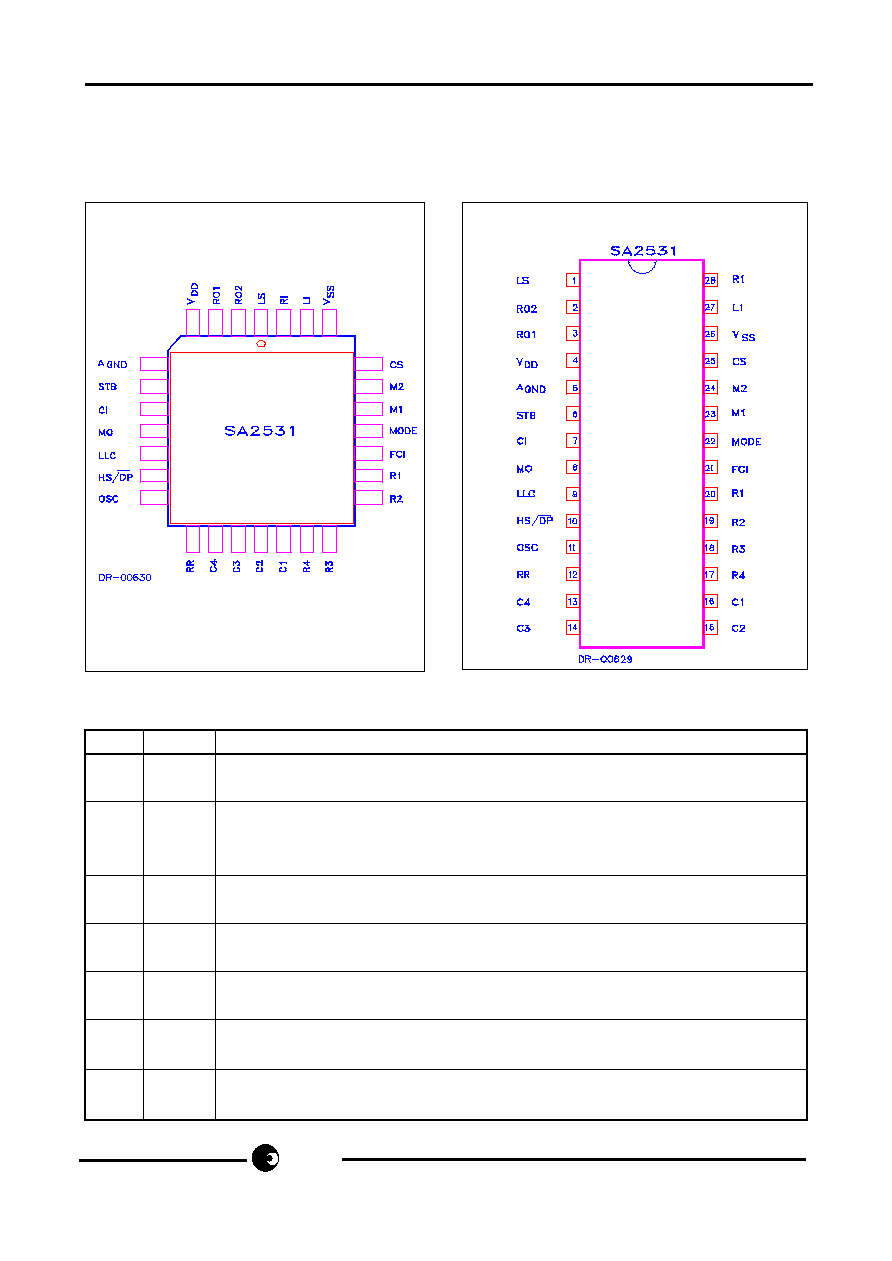
PIN CONFIGURATIONS
PACKAGE
Available in 28 pin DIP and PLCC
PIN DESCRIPTION
Pin# Symbol Function
23
M1
Microphone Inputs
24
M2
Differential inputs for the microphone (electret).
3
RO1
Receiver Outputs
2
RO2
These are the outputs for driving a dynamic earpiece with an impedance
of 150 to 300
5
A
GND
Analogue Ground
This is the analog ground for the amplifiers.
28
RI
Receive Input
This is the input for the receive signal.
6
STB
Side Tone Balance Input
This is the input for side tone cancellation.
1
LS
Line Current Sense Input
This is the input for sensing the line current.
27
LI
Line Input
This input is used for power extraction and line current sensing.
28 Pin PLCC
28 Pin DIP
sames
SA2531 A/B/C/E/G/U
3/24
Pin# Symbol Function
25
CS
Current Shunt Control Output
This N-channel open drain output controls the external high power shunt
transistor for the modulation of the line voltage and for shorting the line
during make period of pulse dialling.
4
V
DD
Positive Voltage Supply
This is the supply pin for the circuit.
26
V
SS
Negative Power Supply
8
MO
Melody Output
Pulse Density Modulated output of the melody generator for tone ringer. At
high impedance when not active.
21
FCI
Frequency Comparator Input
This is a Schmitt trigger input for ring frequency discrimination. Disabled
during off-hook.
10
HS/DP
Hook Switch Input and Dial Pulse Output
This is an I/O that is pulled high by the hook switch when off- hook. An open
drain pulls it low during break periods of pulse dialling and flash.
11
OSC
Oscillator Input
Oscillator pin for Xtal or ceramic resonator (3.58 MHz). Recommended part
is the Murata CSA3.5MG312AM.
9
LLC
Line Loss Compensation
Select pin for the loss compensation.
OPEN = None V
DD
= 45-75mA V
DD
= 20-50mA
12
RR
Repetition Rate
Select pin for repetition rate of melody for the Tone rinser.
22
MODE
Signalling Mode Select Input
Mode pin
Function
High
LD mode, 10pps, M:B = 33:66 (J:20pps)
Open
MFonly
Low
LD mode, 10pps, M:B = 40:60 (J:20pps, M:B = 33:66)
20
R1
Keyboard Rows
19
R2
18
R3
17
R4
16
C1
Keyboard Columns
15
C2
14
C3
13
C4
7
CI
Complex Impedance Input
Input pin for the capacitor in the complex impedance

4/24
SA2531 A/B/C/E/G/U
sames
FUNCTIONAL DESCRIPTION
Power On Reset
The on chip power on reset circuit monitors the supply voltage (V
DD
). When V
DD
rises above
approx. 1.2V, a power on reset occurs to assure correct start-up and the RAM is cleared.
DC Conditions
The normal operating range is from 13mA to 100 mA. Operating range with reduced
performance is from 5mA to 13mA. In the operating range all functions are operational.
At line currents below 13mA the SA2531 provided an additional scope below 4.5V to allow
parallel operation. (See Figure 12).
The dc characteristic (excluding diode bridge and Pulsing transistors) is determined by the
voltage at LI and the resistor R1 as follows:
VLS = VLI + I
Line
.R1
The voltage at LI is 4.5V.
During pulse dialling the speech circuit and other parts of the device not required are in a
power down mode to save current. The CS pin is pulled to V
SS
in order to turn the external
shunt transistor on to keep a low voltage drop at the LS pin during make periods.
AC Impedance
The Characteristic or Output impedance of the SA2531 is set within the IC and adjusted by
Mask Options. Available options are for 600
and 1000
. When the 1000
option is selected
then a capacitor may be added to the circuit at pin CI to add a reactive element and make the
output impedance complex.
Oscillator
All the Timing Functions of the SA2531 are based on a Clock Frequency of 3.58MHz. A crystal
or ceramic resonator of this frequency should be connected to the OSC pin. In practise minor
deviations from the nominal frequency may occur due to the characteristics of the frequency
reference device used and so it is recommended that care is taken in the selection of
components.
Typically a small value capacitor (
47pF) should be connected in parallel with the Frequency
Reference to ensure start-up and/or operation at the nominal frequency.
Speech Circuit
The speech circuit consists of a transmit and a receive path born with soft clip, mute, line loss
compensation and side tone cancellation.
Transmit
The gain of the transmit from M1/M2 to LS is 35dB for 600
versions and 37dB for 1000
versions (see test circuit figure 5). The microphone input is differential with an input
impedance of 25 k
.
The soft clip circuit limits the output voltage at LI to 2.0V
PEAK
(see figures 8 & 9). The attack
time is 30µs/6dB and the decay time is 20 ms/6 dB. When mute is active, during dialling
sames
SA2531 A/B/C/E/G/U
5/24
or after pressing the MUTE key, the gain is reduced by > 60 dB.
Receive
The receive input is the differential signal of RI and STB. The gain of the receive path
is 2 dB (test circuit figure 5) with differential outputs, RO1/RO2 (0dB on 1000
versions).
When mute is active during dialling the gain is reduced by > 60dB. During DTMF dialling
a MF comfort tone is applied to the receiver. The comfort tone is the DTMF signal with
a level that is -30dB relative to the line signal.
The receive gain can be adjusted under user control by using the volume control keys (not
on SA2531D). The VOL key gives a 4dB increase or returns the gain to normal in a Toggle
Function. Alternatively the + and - keys may be used. The + key increases the gain to
a maximum of +6dB while the - key reduces the gain to a minimum of -4dB. Each press
of the keys changes the gain by approximately 2dB.
The gain is reset by the next on-hook.
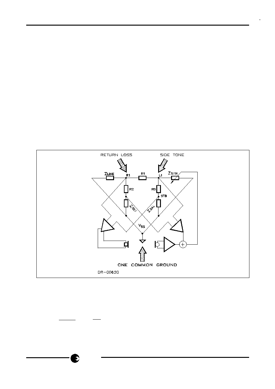
Side Tone
Side Tone is controlled along with Return Loss by a Double Balance Bridge as shown in
Fig. 1.
Figure 1
Double balance bridge (return loss and side tone) with one common ground
A good side tone cancellation is achieved by using the following equation:
ZBAL =
R5
ZLINE
R1