
sames
SA9604A
PDS039-SA9604A-001
REV. 5
29-05-00
FEATURES
s
Performs bidirectional active and
reactive power/energy measurement
s
Voltage and frequency measurement
s
Individual phase information
accessable
s
SPI communication bus
s
Meets the IEC 521/1036 Specification
requirements for Class 1 AC Watt hour
meters
s
Protected against ESD
s
Uses current transformers for current
sensing
s
Excellent long term stability
s
Operates over a wide temperature
range
s
Precision Voltage Reference on-chip
THREE PHASE BIDIRECTIONAL POWER/ENERGY
METERING IC WITH SERIAL SPI INTERFACE
SA9604A
1/20
PIN CONNECTIONS
DESCRIPTION
The SAMES SA9604A Bidirectional Three
Phase Power/Energy metering integrated
circuit has a serial interface, ideal for use
with a �-Controller. The SA9604A performs
the calculation for active and reactive power
or energy, mains voltage sense and
frequency.
The measurements performed and the
resultant register values are provided for
individual phases.
The integrated values for active and reactive
energy, as well as the mains voltage sense
and frequency information, are accessable
through the SPI as 24 bit values.
This innovative universal three phase power/
energy metering integrated circuit is ideally
suited for energy calculations in applications
such as primary industrial metering and
factory energy metering and control.
The SA9604A integrated circuit is available
in both 20 pin dual-in-line plastic (DIP-20),
as well as 20 pin small outline (SOIC-20)
package types.
Package: DIP-20
SOIC-20
DD
O SC1
F1 50
SCK
D0
DR-01306
7
8
9
10
IIP 2
IIN 2
IVP3
IIP 3
IIN 3
V
1
2
6
4
5
3
O SC2
SS
V
14
CS
DI
13
12
11
VREF
IVP2
IVP1
20
G ND
IIN 1
IIP 1
19
18
17
16
15
SA9604A
sames
2/20
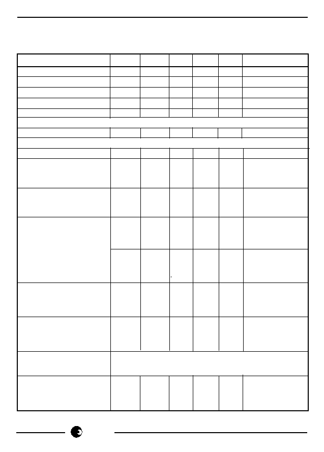
ABSOLUTE MAXIMUM RATINGS*
Parameter
Symbol
Min
Max
Unit
Supply Voltage
V
DD
-V
SS
-0.3
6.0
V
Current on any pin
I
PIN
-150
+150
mA
Storage Temperature
T
STG
-40
+125
�C
Operating Temperature
T
O
-40
+85
�C
* Stresses above those listed under "Absolute Maximum Ratings" may cause permanent
damage to the device. This is a stress rating only. Functional operation of the device
at these or any other condition above those indicated in the operational sections of this
specification, is not implied. Exposure to Absolute Maximum Ratings for extended
periods may affect device reliability.
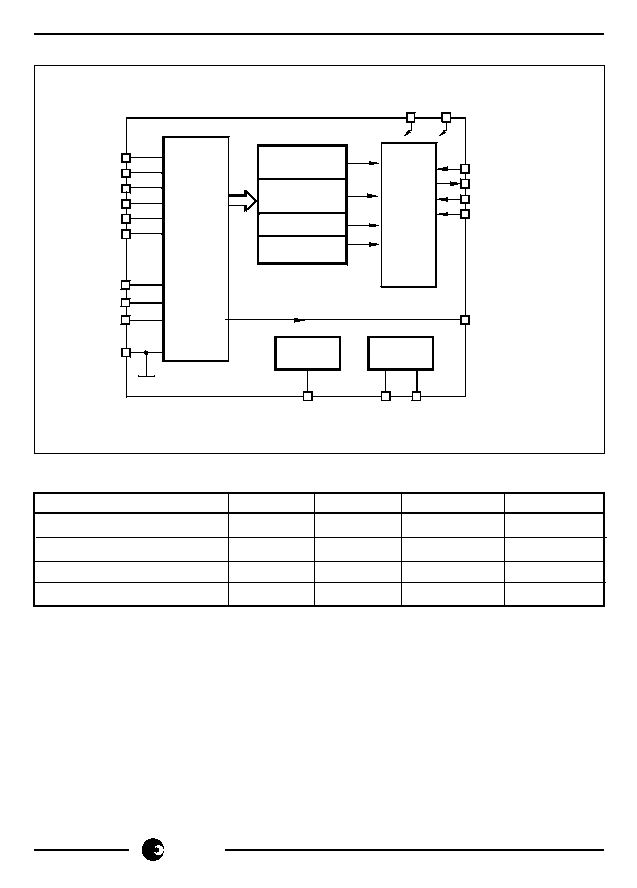
BLOCK DIAGRAM
ACTIVE
ENER GY
VOLTAGE
FREQU ENC Y
REAC TIVE
ENER GY
VOLTAGE
REF.
A N A LO G
S IG N A L
P R O C E S -
S IN G
I VP2
D R -01 3 0 7
G ND
I VP3
II P3
II N3
I VP1
II P1
II N1
II P2
II N2
O SC2
VREF
O SC1
O S C
F 150
S P I
DD
V
CS
SCK
DO
DI
VSS
SA9604A
sames
3/20
ELECTRICAL CHARACTERISTICS
(V
DD
= 2.5V, V
SS
= -2.5V, over the temperature range -10�C to +70�C
#
, unless otherwise
specified.)
Parameter
Symbol
Min
Typ
Max
Unit
Condition
Operating temp. range
T
O
-25
+85
�C
Supply Voltage: Positive
V
DD
2.25
2.75
V
Supply Voltage: Negative
V
SS
-2.75
-2.25
V
Supply Current: Positive
I
DD
8
10
mA
Supply Current: Negative
I
SS
8
10
mA
Current Sensor Inputs (Differential)
Input Current Range
I
II
-25
+25
�A
Peak value
Voltage Sensor Input (Asymetrical)
Input Current Range
I
IV
-25
+25
�A
Peak value
Pin DO
Low Voltage
V
OL
V
SS
+1
V
I
OL
= 5mA
High Voltage
V
OH
V
DD
-1
V
I
OH
= -2mA
Pin DI
High Voltage
V
IH
V
DD
-1
V
Low Voltage
V
IL
V
SS
+1
V
V
IN
= V
SS
Pin SCK
High Voltage
V
IH
V
DD
-1
V
Low Voltage
V
IL
V
SS
+1
V
V
IN
= V
SS
f
SCK
800
kHz
t
LO
0.6
�s
t
HI
0.6
�s
Pin CS
High Voltage
V
IH
V
DD
-1
V
Low Voltage
V
IL
V
SS
+1
V
V
IN
= V
SS
Pin F150
Low Voltage
V
OL
V
SS
+1
V
I
OL
= 5mA
High Voltage
V
OH
V
DD
-1
V
I
OH
= -2mA
Oscillator
Recommended crystal:
TV colour burst crystal f = 3.5795 MHz
Pin VREF
With R = 47k
Ref. Current
-I
R
22.5
25
27.5
�A
connected to V
SS
Ref. Voltage
V
R
1.1
1.3
V
Reference to V
SS
#
Extended Operating Temperature Range available on request.
SA9604A
sames
4/20
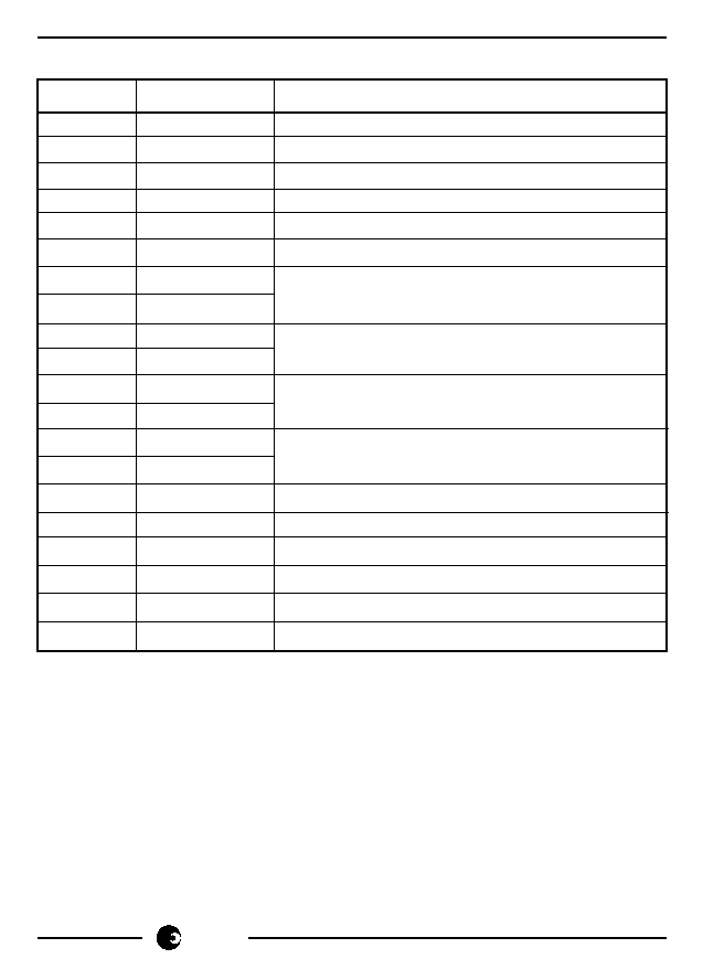
PIN DESCRIPTION
Pin
Designation
Description
16
GND
Ground
6
V
DD
Positive Supply Voltage
14
V
SS
Negative Supply Voltage
17
IVP1
Analog input for Voltage: Phase 1
20
IVP2
Analog input for Voltage: Phase 2
3
IVP3
Analog input for Voltage: Phase 3
19
IIN1
Inputs for Current sensor:Phase 1
18
IIP1
2
IIN2
Input for Current sensor: Phase 2
1
IIP2
5
IIN3
Input for Current sensor: Phase 3
4
IIP3
10
OSC1
Connections for crystal or ceramic resonator
11
OSC2
(OSC1 = Input; OSC2 = Output)
9
DO
Serial Interface Out
12
DI
Serial Interface In
8
SCK
Serial Clock In
13
CS
Chip Select (Active High)
7
FM150
Voltage Sense Zero Crossover
15
VREF
Connection for current setting resistor
FUNCTIONAL DESCRIPTION
The SA9604A is a CMOS mixed signal Analog/Digital Integrated Circuit, which performs
the measurement of active power, reactive power, voltage and frequency.
Internal offsets are eliminated through the use of cancellation procedures. The SA9604A
integrates the measured active and reactive power consumption and the average mains
voltage into 24 bit integrators, which are accessable via the SPI bus. The mains
frequency information is also available as a 24 bit register value.
The zero crossover of each voltage sense input is signalled on the FM150 (pin 7) output.
This output of 150Hz will allow monitoring by a microcontroller to synchronise with internal
timing for data aquisition. Refer to 5.5 for further information.
The SA9604A has tristate output to allow connection of more than one metering device
on a single SPI bus.
SA9604A
sames
5/20
1.
Power calulation
In the Application Circuit (Figure 1), the voltages from Line 1, Line 2 and Line 3, are
converted to currents and applied to the voltage sense inputs IVN1, IVN2 and IVN3.
The current levels on the voltage sense inputs are derived from the mains voltage
(3 x 230 V
AC
) being divided down through voltage dividers to 14V
RMS
. The resulting
input currents into the A/D converters are 14�A
RMS
through the resistors R
15
, R
16
and
R
17
.
For the current sense inputs, the voltages across the current transformers terminating
resistors are converted to currents of 16�A
RMS
for rated conditions, by means of
resistors R
8
, R
9
(Phase 1); R
10
, R
11
(Phase 2); and R
12
, R
13
(Phase 3).
The signals providing the current information are applied to the current sensor
inputs: IIN1; IIP1; IIN2; IIP2; IIN3; and IIP3.
2.
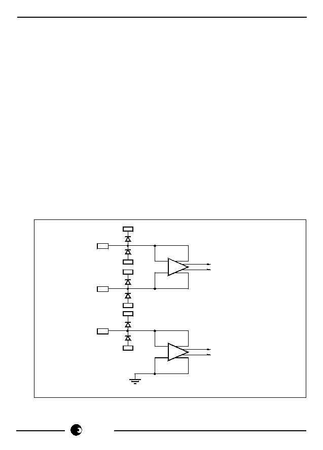
Analog Input Configuration
The input circuitry of the current and voltage sensor inputs are illustrated below.
These inputs are protected against electrostatic discharge through clamping
diodes.
The feedback loops from the outputs of the amplifiers A
I
and A
V
generate virtual
shorts on the signal inputs. Exact copies of the input currents are generated for the
following analog signal processing circuitry.
I V P
DR -0 1 3 0 8
VOL T AGE
SE NS OR
IN PU T
SS
V
I I N
I I P
CU RR EN T
SE NS OR
IN PUT S
DD
V
SS
V
SS
V
DD
V
DD
V
GN D
A
V
A
I
3.
Electrostatic Discharge (ESD), Protection
The SA9604A Integrated Circuits inputs/outputs are protected against ESD.