
Page 1
OCT. 26, 2001
GENERAL DESCRIPTION
SM5272B is a remote control decoder paired
with SM5262B utilizing CMOS Technology.
It has 12-bit tri-state address pins providing a
maximum of 531,411 (or 3
12
) address codes;
thereby, drastically reducing any code
collision and unauthorized code scanning
possibilities. SM5272B is available in
several options to suit every application
needs : variable number of data output pins,
latch or momentary output type.
FEATURES
* CMOS Technology
* Low power consumption
* Very high noise immunity
* Up to 12 tri-State code address pins
* Up to 6 data pins
* Wide range of operating voltage:
Vcc= 2.5 ~ 9 Volts
* Single resistor oscillator
* Latch or momentary output type
* Available in DIP and SOP package
APPLICATIONS
* Garage door
* Toys
* Remote control for industrial use
BLOCK DIAGRAM
Signal
Re-Shap
DIN
VT
A0
A5
OSC1
Timing
Generator
OSC
OSC2
Address
Data
A6/D5 A11/D0
Address
Compare
Data
Compare
Decode
SM5272B
3
12
RF DECODER
S
AM
H
OP
Microelectronics Corp.

Page 2
OCT. 26, 2001
PIN ASSIGNMENTS ( DIP )
18 Vcc
17 VT
16 OSC1
15 OSC2
14 DIN
13 A11
12 A10
11 A9
10 A8
Vss 9
A0 1
A1 2
A2 3
A3 4
A4 5
A5 6
A6 7
A7 8
SM5272B
18 Vcc
17 VT
16 OSC1
15 OSC2
14 DIN
13 D0
12 D1
11 A9
10 A8
Vss 9
A0 1
A1 2
A2 3
A3 4
A4 5
A5 6
A6 7
A7 8
SM5272B-M2/L2
18
Vcc
17
VT
16
OSC1
15
OSC2
14
DIN
13
D0
12
D1
11
D2
10
A8
Vss 9
A0 1
A1 2
A2 3
A3 4
A4 5
A5 6
A6 7
A7 8
SM5272B-M3/L3
18 Vcc
17 VT
16 OSC1
15 OSC2
14 DIN
13 D0
12 D1
11 D2
10 D3
Vss 9
A0 1
A1 2
A2 3
A3 4
A4 5
A5 6
A6 7
A7 8
SM5272B-M4/L4
18 Vcc
17 VT
16 OSC1
15 OSC2
14 DIN
13 D0
12 D1
11 D2
10 D3
Vss 9
A0 1
A1 2
A2 3
A3 4
A4 5
A5 6
A6 7
D4 8
SM5272B-M5/L5
18 Vcc
17 VT
16 OSC1
15 OSC2
14 DIN
13 D0
12 D1
11 D2
10 D3
Vss 9
A0 1
A1 2
A2 3
A3 4
A4 5
A5 6
D5 7
D4 8
SM5272BM6/L6
SM5272B
3
12
RF DECODER
S
AM
H
OP
Microelectronics Corp.

20 Vcc
19 VT
18 OSC1
17 OSC2
16 DIN
15 D0
14 D1
13 D2
12 D3
11 NC
SM5272BS-M5/L5
A0 1
A1 2
A2 3
A3 4
A4 5
A5 6
A6 7
D4 8
Vss 9
NC 10
Page 3
OCT. 26, 2001
PIN CONFIGURATION ( SOP )
A0 1
A1 2
A2 3
A3 4
A4 5
A5 6
D5 7
D4 8
Vss 9
NC 10
SM5272BS
20 Vcc
19 VT
18 OSC1
17 OSC2
16 DIN
15 A11
14 A10
13 A9
A0 1
A1 2
A2 3
A3 4
A4 5
A5 6
A6 7
A7 8
12 A8
Vss 9
11 NC
NC 10
A0 1
A1 2
A2 3
A3 4
A4 5
A5 6
A6 7
A7 8
Vss 9
NC 10
SM5272BS-M2/L2
20 Vcc
19 VT
18 OSC1
17 OSC2
16 DIN
15 D0
14 D1
13 A9
12 A8
11 NC
SM5272BS-M4/L4
20 Vcc
19 VT
18 OSC1
17 OSC2
16 DIN
15 D0
14 D1
13 D2
A0 1
A1 2
A2 3
A3 4
A4 5
A5 6
A6 7
A7 8
12 D3
Vss 9
11 NC
NC 10
SM5272BS-M6/L6
20 Vcc
19 VT
18 OSC1
17 OSC2
16 DIN
15 D0
14 D1
13 D2
12 D3
11 NC
SM5272BS-M3/L3
A0 1
A1 2
A2 3
A3 4
A4 5
A5 6
A6 7
A7 8
Vss 9
NC 10
20 Vcc
19 VT
18 OSC1
17 OSC2
16 DIN
15 D0
14 D1
13 D2
12 A8
11 NC
SM5272B
3
12
RF DECODER
S
AM
H
OP
Microelectronics Corp.

1
2
3
4
5
6
7
A0
A1
A2
A3
A4
A5
A6/D5
I
I
I
I
I
I / O
Address input, each pin can be set to "0",
"1" , or floating.
Address input or data output.
Address input or data output.
8
9
10
A7/D4
Vss
A8/D3
I / O
POWER
I / O
11
12
A9/D2
A10/D1
I / O
I / O
13
A11/D0
I / O
14
DIN
I
Receive from Rf module.
Page 4
OCT. 26, 2001
I
15
OSC1
Resistor connected between these two pins
determine the system clock.
16
OSC2
17
VT
Valid transmission indication.
18
V
DD
Positive power supply.
I
O
O
POWER
PIN FUNCTION
No.
Pin Name
I/O
Function
Negative power supply.
SM5272B
3
12
RF DECODER
S
AM
H
OP
Microelectronics Corp.

Page 5
OCT. 26, 2001
Code Word
A group of Code Bits is called a code Word. A Code Word consists of 12 Address plus Data
bits followed by one Sync Bit. The 12 AD bits are interpreted as either address or data bits
depending on the SM5272B version used. Please refer to the diagrams below:
SM5272B
SM5272B-M2/L2
A0
A1
A2
A3
A4
A5
A6
A7
A8
A9
A10 A11
SYNC
A0
A1
A2
A3
A4
A5
A6
A7
A8
A9
D1
D0
SYNC
SM5272B-M4/L4
A0
A1
A2
A3
A4
A5
A6
A7
D3
D2
D1
D0
SYNC
SM5272B-M5/L5
A0
A1
A2
A3
A4
A5
A6
D4
D3
D2
D1
D0
SYNC
SM5272B-M6/L6
A0
A1
A2
A3
A4
A5
D5
D4
D3
D2
D1
D0
SYNC
One Complete Code Word
SM5272B-M3/L3
A0
A1
A2
A3
A4
A5
A6
A7
A8
D2
D1
D0
SYNC
SM5272B
3
12
RF DECODER
S
AM
H
OP
Microelectronics Corp.
Page 6
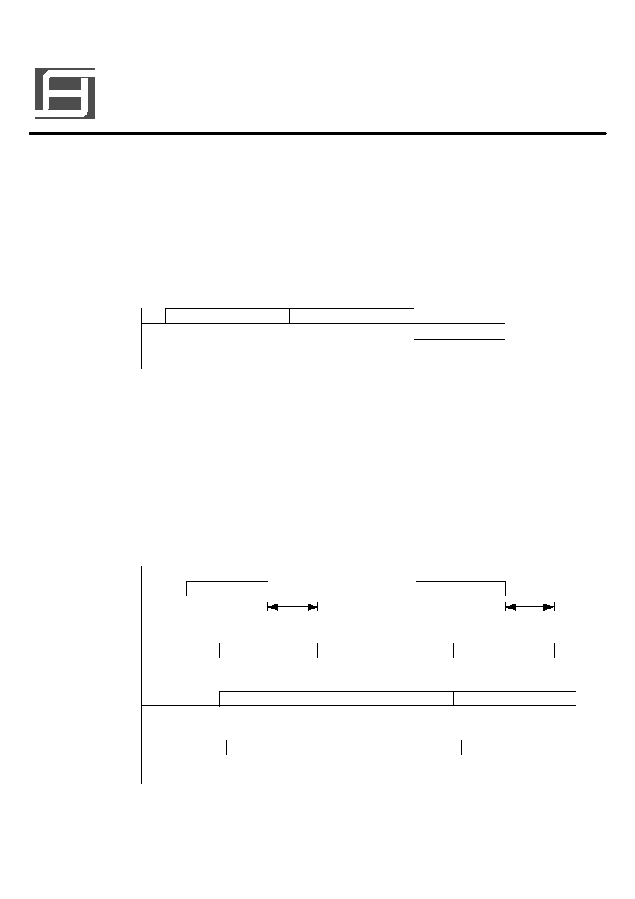
Valid Transmission
After Power On SM5272B enters the Search Address mode, if SM5272B finds 2 consecutive
Address that matches the Address Pin setting of SM5272B then it will set VT high.
If VT is set high, SM5272B is still in search Address. After 2 consecutive Address that do not
match the setting on SM5272B, SM5272B will disable VT.
The timing are shown in the following diagram.
Latch or Momentary Data Output Type
After Power On SM5272B is set in Address search mode, if SM5272B finds 2 consecutive
Address that matches the Address setting of SM5272B. SM5272B will enter Data Compare
mode. It will compare perviously 2 receive data, if they match each then SM5272B will set VT
high and send data O/P.
SM5272B re-enters Address search mode, after 2 consecutive Address that do not match the
setting on SM5272B will disable VT and momentary's data but keep Latch's data intact.
1st Address
S
2nd Address
S
VT
DIN
OCT. 26, 2001
DIN
DATA WORDS
DATA WORDS
T
T
DATA OUTPUT X
DATA OUTPUT Y
DATA PINS
(Momentary)
DATA OUTPUT X
DATA OUTPUT Y
DATA PINS
(Latch)
VT
T= 2 CODE WORD WIDTH
SM5272B
3
12
RF DECODER
S
AM
H
OP
Microelectronics Corp.
Page 7
OCT. 26, 2001
OPERATION FLOWCHART
After Power On SM5272B enters the Search
Address mode, if SM5272B finds 2 consecutive
Address that matches the Address Pin setting
of SM5272B, it will set VT high.
It VT is set high, SM5272B is still in search
Address. After 2 consecutive Address that do
not match the setting on SM5272B, SM5272B
will disable VT.
Power ON
Address
match?
Set VT
Address
match?
Address
match?
Address
match?
Disable VT
NO
YES
YES
NO
YES
YES
NO
NO
SM5272B
3
12
RF DECODER
S
AM
H
OP
Microelectronics Corp.

Page 8
OCT. 26, 2001
DECODER WITH DATA OUTPUT PINS
After Power On SM5272B is set in Address
search mode, if SM5272B finds 2 consecutive
Address that matches the Address setting of
SM5272B.
SM5272B will enter Data Compare mod. It will
compare previously 2 received data, if they
match then SM5272B will set VT high and send
data O/P.
SM5272B re-enters Address search mode, after
2 consecutive Address that do not match
setting on SM5272B will disable VT and
momentary's data but keep Latch's data intact.
Power ON
Address
match?
Address
match?
YES
YES
NO
NO
Data match?
Address
match?
Address
match?
Disable VT and Remove the
Momentary data.
But keep the Latch Type
data intact.
NO
YES
YES
NO
NO
Active VT and
O/P data
YES
SM5272B
3
12
RF DECODER
S
AM
H
OP
Microelectronics Corp.

Page 9
OCT. 26, 2001
Single Resistor Oscillator
SM5272B's oscillator be constructed by connecting a resistor between OSC1 and OSC2 pin.
SM5272B's OSC frequency must be 1.4 to 6.8 times more than SM5262B.
Encoder OSC Frequency
SM5272B
3
12
RF DECODER
S
AM
H
OP
Microelectronics Corp.
Decoder OSC Frequency
Suggested oscillator resistor of SM5262B/ SM5272B:
SM5262B
SM5272B
4.7M OHM
750K OHM
3.0M OHM
390K OHM
2.2M OHM
270K OHM
1.2M OHM
160K OHM
R = 510K
R = 1.2 M
R = 2.7 M
R = 3.0 M
R = 3.3 M
R = 4.3 M
100
KHz
0
6
9
12
15 VOLTAGE
90
80
70
60
50
40
30
20
10
2.5
VOLTAGE
R = 100 K
R = 300 K
R = 620 K
R = 680 K
R = 820 K
R = 1.0 M
300
0
6
9
200
100
50
250
2.5
180
KHz

Page 10
DC ELECTRICAL CHARACTERISTICS
OCT. 26, 2001
Conditions
Unit
Limit
Symbol
Min. Typ. Max.
V
V
CC
2.5
9
Vcc = 12 V
OSC stop
A0 ~ A11 open
A
I
STB
0.02
0.3
I
OH
I
OL
Parameter
Supply Voltage
Standby Current
Data Output
Driving Current
Data Output
Sinking Current
SM5272B
3
12
RF DECODER
S
AM
H
OP
Microelectronics Corp.
Vcc = 5V
V
OH
= 1V
mA
8
Vcc = 9V
V
OH
= 1.8V
mA
20
Vcc = 5V
V
OH
= 4V
mA
-3.5
Vcc = 9V
V
OH
= 7.2V
mA
-7.1

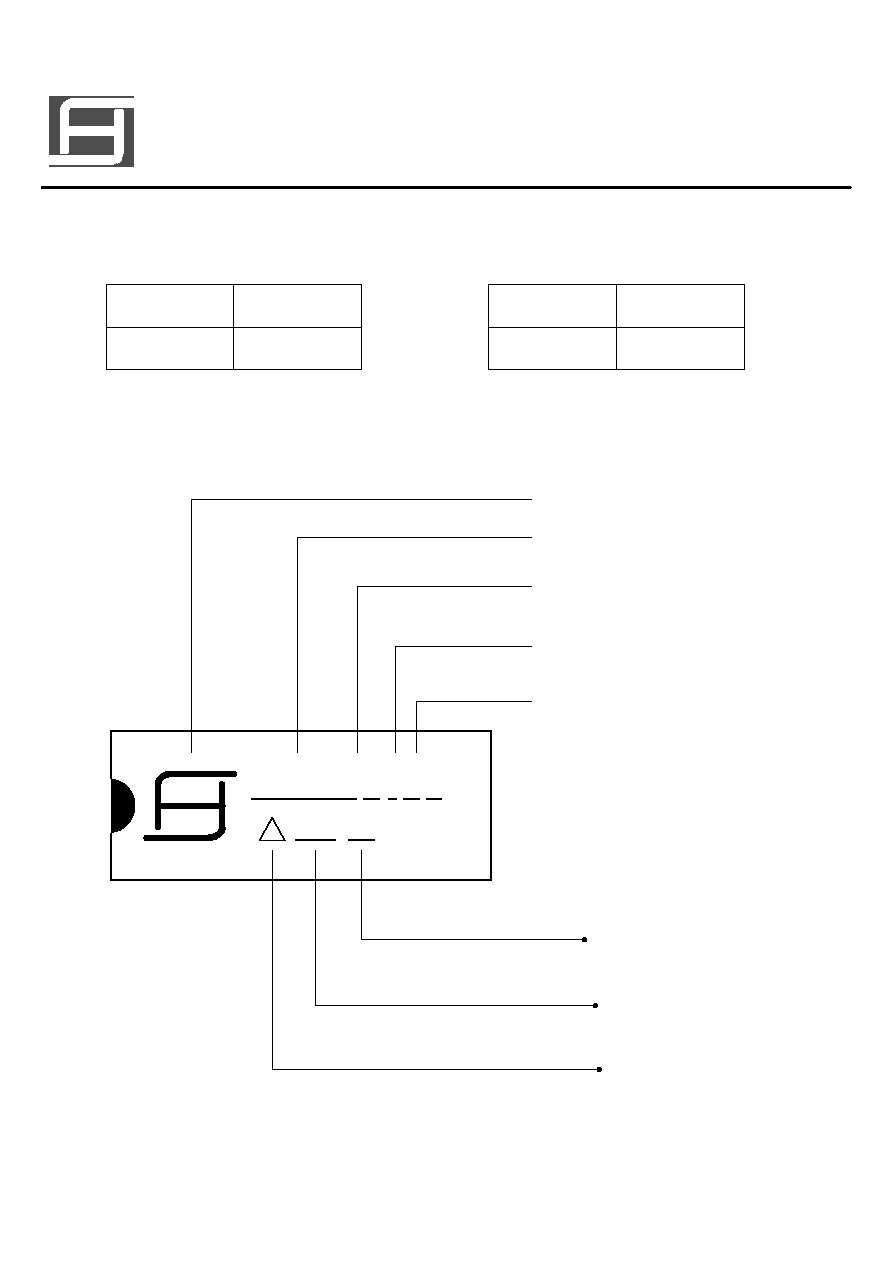
Vss
A0
A1
A2
A3
A4
A5
A6
A7
V
DD
VT
OSC1
OSC2
DIN
A11
A10
A9
A8
RF
Receiver
SM5272B
VT
ROSC
APPLICATION CIRCUIT
Page 11
OCT. 26, 2001
SM5272B
3
12
RF DECODER
S
AM
H
OP
Microelectronics Corp.
Page 12
ORDERING INFORMATION
Part No.
Package
SM5272B
18 Pin DIP
Part No.
Package
SM5272BS
20 Pin SOP
OCT. 26, 2001
SM5272B S
- X X
Logo
Empty: DIP TYPE
S: SO Package
M:Momentary type
L: Latch type
None: 0 Data Bits
2:Two Data Bits
3:Three Data Bits
4:Four Data Bits
5:Five Data Bits
6:Six Data Bits
Product No.
SM5272B
3
12
RF DECODER
S
AM
H
OP
Microelectronics Corp.
Date Code
Serial Number
ESD Protection Mark
xxx xx