
Page 1
GENERAL DESCRIPTION
SM6311 is a Vacuum Fluorescent Display (VFD)
Controller driven on a 1/8 to 1/16 duty factor.
Twelve segment output lines, 8 grid output lines, 8
segment/grid output drive lines, key scan, one
d i s p l a y m e m o r y , I C c o n t r o l c i r c u i t a r e a l l
incorporated in a single chip. This SM6311 is ideal
a s a p e r i p h e r a l d e v i c e o f a s i n g l e c h i p
microcomputer.
FEATURES
* Multiple Display Modes
* High Voltage Output
* Key Scanning
* General Purpose Input Ports (4 bit)
* Dimming Circuitry (8 segment)
* LED Display Ports(5 outs, 20mA max)
* No external Resistors Needed for Driver
Outputs
* Serial Interface for controller
APPLICATIONS
* Audio System
* Car Stereo
* VCD
* DVD
* VCR
* TV
PIN DIAGRAM ( TOP VIEW)
V.1.2, MAY,2003
SM6311
SAMHOP Microelectronics Corp.
VFD CONTROLLER / DRIVER
V
DD
Sg4/KS4
Sg3/KS3
Sg2/KS2
Sg1/KS1
Sg8/KS8
Sg7/KS7
Sg6/KS6
Sg5/KS5
Sg9/KS9
Sg10/KS10
Sg11/KS11
Sg12/KS12
39
35
36
37
38
31
32
33
34
30 29 28 27
14
18
17
16
15
22
21
20
19
23
24
25
26
52
48
49
50
51
44
45
46
47
43
42
41
40
OSC
LED3
LED2
LED1
GND
G1
V
DD
LED5
LED4
G2
G3
G4
G5
S1
S2
D
OUT
S3
STB
CLK
NC
D
IN
K1
K2
K3
K4
S4
1
5
4
3
2
9
8
7
6
10 11 12 13
Sg13/G16
G6
G7
Sg19/G10
G8
Sg17/G12
Sg18/G11
V
DD
V
EE
Sg16/G13
Sg15/G14
Sg14/G15
Sg20/G9

BLOCK DIAGRAM
Page 2
V.1.2, MAY,2003
Serial
Data
I/F
OSC
4 bit
Latch
Decoder
Display Memory
20bits*16words
Timing Gen
Key Memory
(12*4)
5 bit Latch
Dimming Ckt
20 bit
Latch
16 bit
Shift
Register
Data
Selector
Grid
Driver
Seg/Grid
Driver
Segment
Driver
LED
1
~ LED
5
SG
1
SG
12
~
SG
13
/
Grid
16
SG
20
/
Grid
9
~
Grid
1
Grid
8
~
S1
S4
~
K1
K4
~
4
4
R
V
DD
D
IN
D
OUT
STB
CLK
20
12
8
8
8
8
16
V
DD
GND V
EE
(+5V) (0V) (-30V)
Power Ckt
SM6311
SAMHOP Microelectronics Corp.
VFD CONTROLLER / DRIVER

Page 3
PIN DESCRIPTION
V.1.2, MAY,2003
FUNCITON DESCRIPTION
Outputs serial data at falling edge of shift clock,
starting from lower bit.
Input serial data at rising edge of shift clock,
starting from lower bit.
Connect this pin to GND of system.
Reads serial data at rising edge, and outputs
data at falling edge.
While STB is low, Data is valid; while STB is
high, CLK is ignored.
Data input to these pins is latched at end of
display cycle.
5V+10%.
Segment output pins (Dual function as key
source).
These pins are selectable for segment or grid
output.
V
DD
-35V max.
Grid output pins
CMOS output. +20 mA max.
Connect resistor for determining oscillation
frequency to this pin.
4 bit general-purpose input port.
7,51
8
9
10 to 13
14, 33, 45
15 to 26
27 to 32
35 to 36
34
37 to 44
46 to 50
52
PIN NO.
5
6
1 to 4
SYMBOL
D
OUT
D
IN
GND
CLK
STB
K1 to K4
V
DD
Sg1/KS1~
Sg12/KS12
Sg12/G16~
Sg20/G9
V
EE
G1~G8
LED1~LED5
OSC
S1 to S4
PIN NAME
Data Output
Data Input
Logic Ground
Clock Input
Strobe
Key data input
Logic Power
Segment/Key
Segment/Grid
Pull Down
Level
Grid
LED Output
Oscillator Pin
Switch Input
SM6311
SAMHOP Microelectronics Corp.
VFD CONTROLLER / DRIVER

Display RAM Address and Display Mode
The display RAM stores the data transmitted from an external device to the SM6311 through the serial
interface, and is assigned addresses as follows, in units of 8 bits :
Only the lower 4 bits of the addresses assigned to Seg
17
through Seg
20
are valid, and the higher 4
bits are ignored.
00 H
L
06 H
L
09 H
L
0C H
L
0F H
L
12 H
L
15 H
L
18 H
L
1B H
L
1E H
L
21 H
L
24 H
L
27 H
L
2A H
L
2D H
L
03 H
L
03 H
U
06 H
U
09 H
U
0C H
U
0F H
U
12 H
U
15 H
U
18 H
U
1B H
U
1E H
U
21 H
U
24 H
U
27 H
U
2A H
U
2D H
U
00 H
U
01 H
L
07 H
L
0A H
L
0D H
L
10 H
L
13 H
L
16 H
L
19 H
L
1C H
L
1F H
L
22 H
L
25 H
L
28 H
L
2B H
L
2E H
L
04 H
L
04 H
U
07 H
U
0A H
U
0D H
U
10 H
U
13 H
U
16 H
U
19 H
U
1C H
U
1F H
U
22 H
U
25 H
U
28 H
U
2B H
U
2E H
U
01 H
U
02 H
L
05 H
L
08 H
L
0B H
L
0E H
L
11 H
L
14 H
L
17 H
L
1A H
L
1D H
L
20 H
L
23 H
L
26 H
L
29 H
L
2C H
L
2F H
L
DIG
1
DIG
2
DIG
3
DIG
4
DIG
5
DIG
6
DIG
7
DIG
8
DIG
9
DIG
10
DIG
11
DIG
12
DIG
13
DIG
14
DIG
15
DIG
16
Seg
1
Seg
4
Seg
8
Seg
12
Seg
16
Seg
20
XX H
L
XX H
U
b
0
b
3
b
4
b
7
Lower 4 bits Higher 4 bits
Page 4
V.1.2, MAY,2003
SM6311
SAMHOP Microelectronics Corp.
VFD CONTROLLER / DRIVER

Page 5
V.1.2, MAY,2003
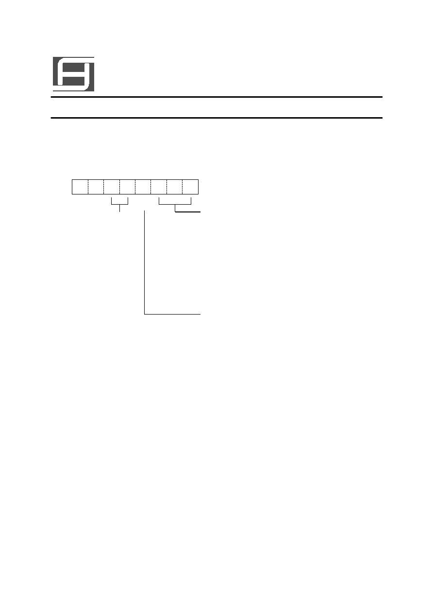
SW DATA
The SW data is read by a read command, starting from the least significant bit. Bits 5 through 8 of the
SW data are 0.
0
0
0
0
b3
b2
b1
b0
sw
1
sw
2
sw
3
sw
4
COMMAND
A command sets the display mode and status of the FIP driver.
The first 1 byte input to the SM6311 through the D
IN
pin after the STB pin has fallen is regarded as
a command.
If STB is made high while a command / data is transmitted, serial communication is initialized, and the
command / data being transmitted is invalid ( however, the command / data already transmitted remains
valid ).
(1) Display mode setting command
The command initializes the SM6311 and selects the number of segments and number of grids ( 1/8
to 1/16 duty, 12 segments to 20 segments ).
When this command is executed, display is forcibly tuned off, and key scanning is also stopped.
To resume display, a display ON command must be executed. If the same mode is selected,
however, nothing is performed.
0
0
b3
b2
b1
b0
MSB
LSB
Dont's care
Selects display mode
0xxx : 8 digits, 20 segments
1000 : 9 digits, 19 segments
1001 : 10 digits, 18 segments
1010 : 11 digits, 17 segments
1011 : 12 digits, 16 segments
1100 : 13 digits, 15 segments
1101 : 14 digits, 14 segments
1110 : 15 digits, 13 segments
1111 : 16 digits, 12 segments
On power application, the 16-digit, 12-segment mode is selected.
LSB
MSB
SM6311
SAMHOP Microelectronics Corp.
VFD CONTROLLER / DRIVER
Page 6
V.1.2, MAY,2003
DISPLAY CONTROL COMMAND
1
0
b3
b2
b1
b0
MSB
LSB
Dont's care
Sets dimming quantity
000 : Sets pulse width to 1/16
001 : Sets pulse width to 2/16
010 : Sets pulse width to 4/16
011 : Sets pulse width to 10/16
100 : Sets pulse width to 11/16
101 : Sets pulse width to 12/16
110 : Sets pulse width to 13/16
111 : Sets pulse width to 14/16
Turns on / off display.
0 : Display off ( key scan contiunes
*
)
1 : Display on
*
: On power application, key scanning is stopped.
SM6311
SAMHOP Microelectronics Corp.
VFD CONTROLLER / DRIVER

SERIAL COMMUNICATION FORMAT
Reception ( command / data write )
STB
D
IN
CLK
b6
b7
b0
b1
b2
1
2
3
7
8
Transmission ( data read )
STB
CLK
1
2
3
4
5
6
1
D
IN
b0
b1
b2
b3
b4
b5
b6
b7
2
3
4
5
6
7
8
D
OUT
b0
b1
b2
b3
b4
b5
t
WAIT
*
Data reading command is set.
Data reading starts.
Because the D
OUT
pin is an N-ch, open-drain output pin, be sure to connect an external pull-up resistor to
this pin ( 1 K
to 10 K
).
*
: When data is read, a wait time t
WAIT
of 1
s
is necessary since the rising of the eighth clock that has
set the command, until the falling of the first clock that has read the data.
Page 7
V.1.2, MAY,2003
SM6311
SAMHOP Microelectronics Corp.
VFD CONTROLLER / DRIVER

ABSOLUTE MAXIMUM RATINGS
RECOMMENDED OPERATING CONDITIONS
(Ta=-20 to +70
o
C, GND=0V)
(Ta=25
o
C, GND=0V)
Page 8
V.1.2, MAY,2003
UNIT
V
V
V
V
mA
mA
PARAMETER
Logic Supply Voltage
Driver Supply Voltage
Logic Input Voltage
VFD Driver Output Voltage
LED Driver Output Current
VFD Driver Output Current
SYMBOL
V
DD
V
EE
V
I
VO
I
OLED
I
OVFD
RATING
-0.5 to +7
V
DD
+0.5 to V
DD
-30
-0.5 to V
DD
+0.5
V
EE
-0.5 to V
DD
+0.5
+25
-40(grid) / -15(segment)
Unit
V
V
V
V
MIN.
4.5
0.7V
DD
0
0
TYP.
5
MAX.
5
V
DD
0.3V
DD
V
DD
-35
PARAMETER
Logic Supply Voltage
Driver Supply Voltage
High-Level Input Voltage
Low-Level Input Voltage
SYMBOL
V
DD
V
EE
V
IL
V
IH
SM6311
SAMHOP Microelectronics Corp.
VFD CONTROLLER / DRIVER

DC/AC ELECTRICAL CHARACTERISTIC
(V
DD
=5V, GND=0V, V
EE
=V
DD
-35V, TA =25, unless otherwise noted)
TIMING CONDITIONS ( Ta=-20 to +70, V
DD
=4.5 to 5.5V )
PARAMETER
SYMBOL
MIN.
TYP.
MAX.
UNIT
TEST CONDITIONS
Clock Pulse Width
PW
CLK
400
ns
Strobe Pulse Width
1
Data Setup Time
t
SETUP
100
Data Hold Time
t
HOLD
100
s
Clock-Strobe Time
1
CLK STB
t
CLK-STB
Wait Time
t
WAIT
1
PW
STB
s
ns
ns
s
CLK CLK
Page 9
V.1.2, MAY,2003
SM6311
SAMHOP Microelectronics Corp.
VFD CONTROLLER / DRIVER
PARAMETER
SYMBOL
MIN.
TYP.
MAX.
UNIT
TEST CONDITIONS
High-Level Output Voltage
V
OHLED
0.9V
DD
V
I
OHLED
=-1mA, LED1 to LED5
Low-Level Output Voltage
V
OLLED
1
V
I
OLLED
=+20mA, LED1 to LED5
Low-Level Output Voltage
V
OLDout
0.4
V
D
OUT
,I
OLDout
=4mA
High-Level Output Current
I
OHSg
-3
mA
V
O=
V
DD
2V, Seg
1 to
Seg
12
High-Level Output Current
V
OHGr
-15
mA
V
O=
V
DD
2V, Grid
1 to
Grid
8
,
Seg
13
/ Grid
16
to Seg
20
/ Grid
9
V
IH
0.7V
DD
V
High-Level Input Voltage
V
IL
0.3V
DD
V
Low-Level Input Voltage
fosc
350
500
650
KHz
R=51K
Oscillation Frequency
SWITCHING CHARACTERISTICS ( Ta=-20 to +70, V
DD
=4.5 to 5.5V, V
EE
=-30V )
PARAMETER
SYMBOL
MIN.
TYP.
MAX.
UNIT
TEST CONDITIONS
Oscillation Frequency
t
OSC
350
500
650
KHz
R=56K
Propagation Delay Time
t
PLZ
300
ns
CLK D
OUT
C
L
=15pF, R
L
=10K
Rise Time
C
L
=300pF
t
PZL
100
ns
t
TZH1
2
s
t
TZH2
0.5
s
Grid
1
to Grid
8
,
Seg
13
/ Grid
16
to
Seg
20
/ Grid
9
Fall Time
t
THZ
120
s
C
L
=300pF, Seg
n
, Grid
n
Maximun Clock Frequency
1
MH
Z
Duty=50%
fmax.
Input Capacitance
C
I
pF
15
Seg
1
to Seg
12

Page 10
V.1.2, MAY,2003
APPLICATIONS
Updating display memory by incrementing address
D
IN
Command 1
Command 2
Command 3
Data 1
Data n
Command 4
CLK
STB
Command 1 : sets display mode
Command 2 : sets data
Command 3 : sets address
Data 1 to n : transfers display data (48 bytes max.)
Command 4 : controls display
Updating specific address
D
IN
Command 1
Command 2
Command 2
Data
Data
CLK
STB
Command 1 : sets date
Command 2 : sets address
Data : display data
SM6311
SAMHOP Microelectronics Corp.
VFD CONTROLLER / DRIVER

PACKAGE SPEC.
52 PINS QFP DIMENSION
Note: Controlling dimensions are in millimeters (MM).
17.20 + 0.25
14.00
26
14
40
52
Index
1
13
1.00
14.00
17.20 +
0.25
39
27
0.35 + 0.1
2.75 + 0.1
1.60
0.8 + 0.2
2.70 + 0.20
Page 11
V.1.2, MAY,2003
SM6311
SAMHOP Microelectronics Corp.
VFD CONTROLLER / DRIVER