
Page 1
The SM6B595 is specifically designed for
USE in LED DISPLAY.
This device contains an 8-bit shift register,
8 bit D-type storage register an d open-drain
NMOS output drivers.
The serial output allows for cascading of the
data from the shift register to additional
devices.
PIN ASSIGNMENTS
GENERAL DESCRIPTION
FEATURES
* Maximum output terminal voltage: 30V.
* Maximum continuous drain current:100mA.
* Typical R
DS(ON) :
5
* Devices are cascadable
* Low power consumption
* Serial data transfer rate: 25 MHz.
SM6B595P
20 PIN DIP
SM6B595F
20 PIN SOP
SM6B595
8-BIT LED DRIVER
S
AM
H
OP
Microelectronics Corp.
SEP, 2002
1
2
3
4
5
6
7
8
9
10
20
19
18
17
16
15
14
13
12
11
NC
VCC
SERIN
OUT0
OUT1
OUT2
OUT3
SRCLR
G
GND
NC
GND
SEROUT
OUT7
OUT6
OUT5
OUT4
SRCK
RCK
GND
1
2
3
4
5
6
7
8
9
10
20
19
18
17
16
15
14
13
12
11
NC
VCC
SERIN
OUT0
OUT1
OUT2
OUT3
SRCLR
G
GND
NC
GND
SEROUT
OUT7
OUT6
OUT5
OUT4
SRCK
RCK
GND

Page 2
PIN DESCRIPTION
SM6B595
8-BIT LED DRIVER
S
AM
H
OP
Microelectronics Corp.
13
Pin NO.
1
2
3
14-17
4-7
8
18
19
20
SRCK
Pin Name
NC
Vcc
SER IN
OUT4~7
OUT0~3
SRCLR
SER OUT
GND
NC
Input terminal of a clock for shift-register. Data transfer through
shift-register on the rising edge of the shift-register clock.
Function Description
No connection
5V supply voltage terminal.
Input terminal of a serial-data for shift-register.
Output terminals.
Output terminals.
Input terminal of clear signal for shift-register. When SRCLR is
low, the input shift-register is cleared.
Output terminal of serial-data for next SER IN terminal.
Ground terminal.
No connection.
9
G
Input terminal of output enable. All outputs (OUT0~7) do off
with "H" level of G-terminal, and do on with "L" level input.
10-11
GND
Ground terminal.
12
RCK
Input terminal of a clock for storage-register. Data transfer
through storage-register on the rising edge of the storage-
register clock.
SEP, 2002

Page 3
BLOCK DIAGRAM
TIMING DIAGRAM
SM6B595
8-BIT LED DRIVER
S
AM
H
OP
Microelectronics Corp.
G
RCK
SRCK
SERIN
SRCLR
SERIAL-OUT
D Q
CK
CLR
D Q
CK
CLR
D Q
CK
CLR
Q D
CK
Q D
CK
Q D
CK
OUT0
OUT1
OUT7
SER IN
SRCLR
RCK
G
Out0
Out1
Out2
Out7
Serial-out
0V
5V
0V
0V
5V
0V
5V
Off
On
Off
5V
Off
Off
On
0V
5V
5V
0V
SRCK
SEP, 2002

TRUTH TABLE
Page 4
SM6B595
8-BIT LED DRIVER
S
AM
H
OP
Microelectronics Corp.
SRCLR
H
H
H
Shift-register
H R
0
R
1
... R
5
R
6
L R
0
R
1
... R
5
R
6
R
0
R
1
R
2
... R
6
R
7
SEROUT
R
6
R
6
R
7
Storage-register
RCK
G
SRCK
L
L L L ... L L
L
X
P
0
P
1
P
2
... P
6
P
7
P
7
X X X ... X X
H
OUT0 OUT1...OUT7
P0 P1 ... P7
H H ... H
SERIN
H
L
X
X
X X X ... X X
X
P0 P1 P2 ... P6 P7
L
R0 R1 R2 ...R6 R7
P : Present state. R : Previous state.
-55 ~ 150
o
C
Rating
7 V
- 0.3 ~ 7V
100 mA
30 V
-40 ~ 125
o
C
Tstg
Storage Temperature
Symbol
VCC
VIN
IOUT
VOUT
Topr
Characteristic
Logic Supply Voltage
Logic Input Voltage
Output Current
Output Voltage
Operating Termerature
MAXIMUM RATINGS (Ta = 25
o
C unless otherwise noted)
SEP, 2002

Page 5
RECOMMENDED OPERATING CONDITIONS
SM6B595
8-BIT LED DRIVER
S
AM
H
OP
Microelectronics Corp.
Characteristic
Unit
Typ. Max.
Symbol
Supply Voltage
Output Voltage
V
V
5.0
5.5
30
V
CC
V
OUT
Output Current
Input Voltage
Set-up Time for SER IN
Hold Time for SER IN
Pulse duration for SER IN
Operating Temperature
o
C
mA
V
V
ns
ns
ns
85
100
0.15Vcc
I
O
V
IH
V
IL
tsetup
t
hold
tw
Topr
Min.
4.5
-40
0.85Vcc
20
20
40
Condition
OUTn
OUTn
SEP, 2002

Page 6
ELECTRICAL CHARACTERISTICS (V
DD
= 5.0V, Ta = 25
o
C unless otherwise noted)
SM6B595
8-BIT LED DRIVER
S
AM
H
OP
Microelectronics Corp.
Symbol
V
(BR)DSX
Characteristic
Output breakdownvoltage
Condition
I
0
=I
m
A
Min.
Typ. Max.
Unit
30
V
SEP, 2002
I
DSX
Off-state leakage current
�A
V
0
=24V, V
cc
= 5.5V
V
0
=24V, V
cc
=5.5V, Tc=125
o
C
V
0
=12V, Vcc= 5.5V
V
0
=12V, Vcc=5.5V, Tc=125
o
C
I
N
I
IH
R
DS(ON)
Static drain-source
on-state resistance
I
IL
V
DS(on)
=0.5V, Ta=85
o
C
90
V
I
= V
cc
=5.5V
�A
I
0
= 100
m
A, V
cc
= 4.5V
5
V
I
= 0, V
cc
=5.5V
-1
Nominal Current
Logic input current
1
mA
�A
0.5
10
0.1
1
5
30
1
3
SER OUT output voltage
V
OH
V
OL
V
V
V
V
Propagation delay
(G-OUTn)
Output rise time
Output fall time
t
PLH
t
PLH
I
o
= 100
m
A, CL=30
PF
150
I
o
= 100
m
A, CL=30
PF
90
t
r
t
f
I
o
= 100
m
A, CL=30
PF
200
I
o
= 100
m
A, CL=30
PF
200
ns
ns
ns
ns
I
OH
= -20�A, V
cc
= 4.5V
I
OH
= -4
m
A, V
cc
= 4.5V
I
OL
=20�A, V
cc
= 4.5V
I
OL
= 4
m
A, V
cc
= 4.5V
4.4
4.49
4.0
4.2
0.005
0.3
0.1
0.5
I
CC
V
CC
=5.5V
20
Logic Supply Current
100
�A

Page 7
0
0
0
TIMING WAVEFORM
SM6B595
8-BIT LED DRIVER
S
AM
H
OP
Microelectronics Corp.
t
W
(SRCK)
t
setup
t
hold
t
p
t
setup
t
W(RCK)
t
p
t
W(G)
t
PLH
t
PHL
t
f
t
r
50%
50%
50%
50%
50%
50%
90%
10%
SRCK
SER IN
SER OUT
RCK
OUT
n
OUT
n
G
G
Low
SEP, 2002
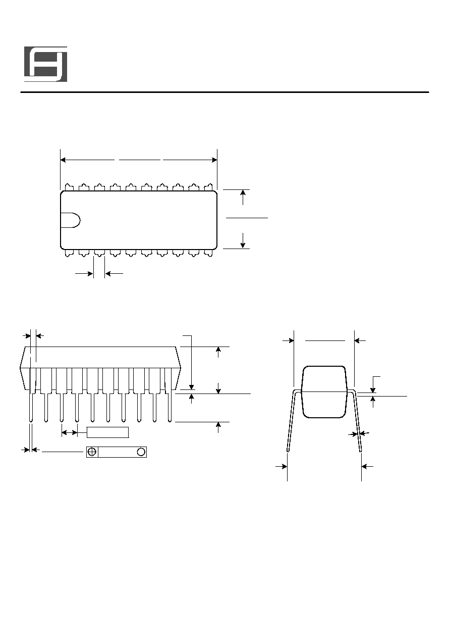
PACKAGE OUTLIN
Page 8
SEP, 2002
SM6B595
8-BIT LED DRIVER
S
AM
H
OP
Microelectronics Corp.
1
10
11
20
0.070 (1.78) MAX
0.260 (6.60)
0.240 (6.10)
0.975 (24.77)
0.940 (23.88)
0.035 (0.89) MAX
0.020 (0.51) MIN
0.200 (5.08) MAX
0.125 (3.18) MIN
Seating Plane
0.021 (0.53)
0.015 (0.38)
0.010 (0.25)
M
0.100 (2.54)
0.430 (10.92) MAX
0.010 (0.25) NOM
Gauge Plane
0.325 (8.26)
0.300 (7.62)
0.015 (0.38)
20 PINS DIP
UNIT : inches (millimeters)

PACKAGE OUTLIN
Page 9
SM6B595
8-BIT LED DRIVER
S
AM
H
OP
Microelectronics Corp.
0.510 (12.95)
0.500 (12.70)
0.020 (0.51)
0.014 (0.35)
0.050 (1.27)
0.010 (0.25)
M
0.419 (10.65)
0.400 (10.15)
0.299 (7.59)
0.291 (7.39)
1
10
11
20
0.012 (0.30)
0.004 (0.10)
0.104 (2.65) MAX
Seating Plane
0.004 (0.10)
0.050 (1.27)
0.016 (0.40)
0.010 (0.25) NOM
Gage Plane
0.010 (0.25)
0
o
- 8
o
20 PINS SOP
UNIT : inches (millimeters)
SEP, 2002