 | –≠–Ľ–Ķ–ļ—ā—Ä–ĺ–Ĺ–Ĺ—č–Ļ –ļ–ĺ–ľ–Ņ–ĺ–Ĺ–Ķ–Ĺ—ā: adc1256x | –°–ļ–į—á–į—ā—Ć:  PDF PDF  ZIP ZIP |
The ADC1256X is a CMOS 12bit analog-to-digital
converter (ADC).
It converts the analog input signal
into 12bit binary digital codes at a maximum
sampling rate of 20MHz.
The device is a monolithic ADC with an on-chip,
high-performance, sample-and-hold Amplifier (SHA)
and current reference.
The structure allows both
differential and single-ended input.
Resolution : 12bit
Maximum Conversion Rate : 20MHz
Package Type : 48TSSOP
Power Supply : 2.5V
Power Consumption : 115mW (typical)
Reference Voltage : 1.75V, 0.75V (dual reference)
Input Range : Ī1V (differential)
Differential Linearity Error : Ī1.0 LSB (Max)
Integral Linearity Error : Ī3.0 LSB (Max)
Signal to Noise & Distortion Ratio : 62dB (Typ.)
Digital Output : CMOS Level
Operating Temperature Range : 0ļC
~ 70
ļC
GENERAL DESCRIPTION
FEATURES
FUNCTIONAL BLOCK DIAGRAM
High Definition TV (HDTV)
Video Applications
CCD Imaging (Copiers, Scanners, Cameras)
Medical Imaging
Digital Communications
TYPICAL APPLICATIONS
12BIT 20MSPS ADC
ADC1256X
SAMSUNG ELECTRONICS Co. LTD
Ver 1.1 (February. 2000)
No responsibility is assumed by SEC for its use nor for any infringements of patents
or other rights of third parties that may result from its use. The content of this
datasheet is subject to change without any notice.
SHA
MDAC2
GAIN=8
MDAC3
GAIN=8
MDAC1
GAIN=8
FLASH
1
FLASH
2
FLASH
3
FLASH
4
4
4
4
4
4
4
4
12
DIGITAL CORRECTION LOGIC
Common Mode
Level Generator
Clock
Generator
MAIN
BIAS
VDD25A1
VSS25A1
VBBA1
VDD25A2
VSS25A2
VBBA2
CML
SPEEDUP
ITEST
STBY
CKIN
AINT
AINC
REFTOP1
REFTOP
REFBOT
REFBOT1
DO[11:0]
[MSB:LSB]
SEC ASIC
ADC1256X
12BIT 20MSPS ADC
ANALOG
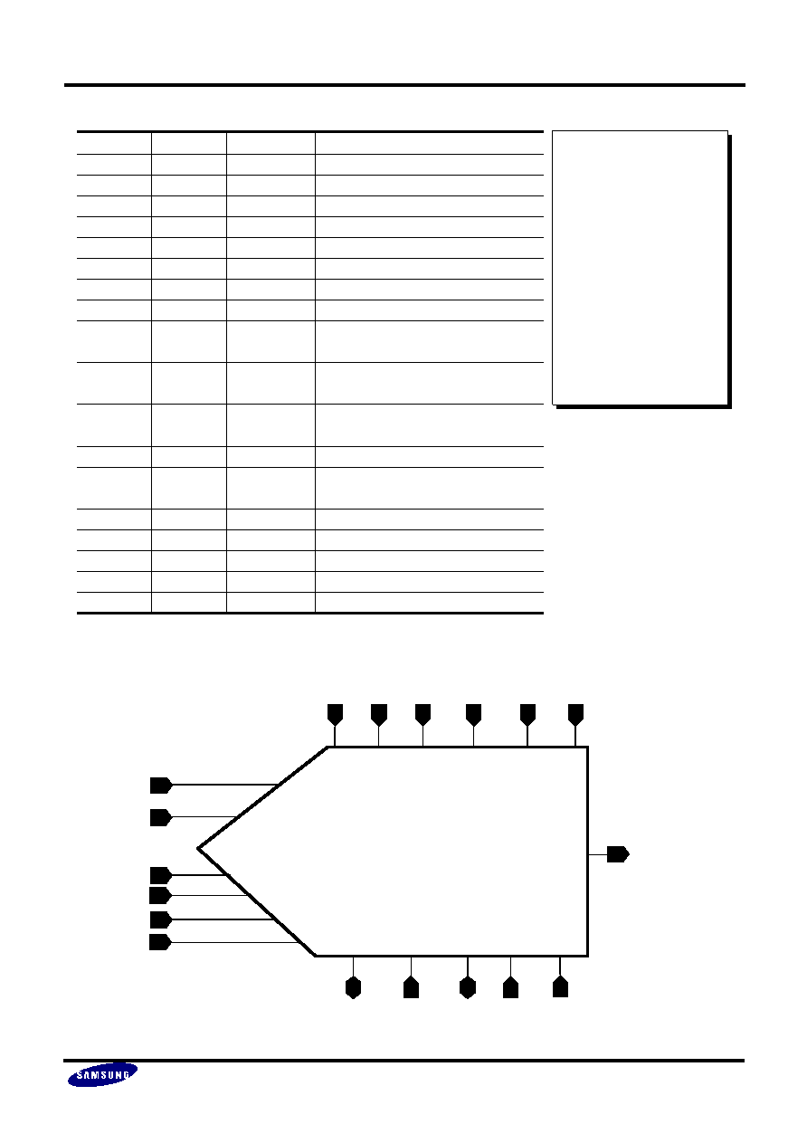
CORE PIN DESCRIPTION
NAME
I/O TYPE
I/O PAD
PIN DESCRIPTION
REFTOP1
AI
piar50_abb
Reference Top Sense (1.75V)
REFTOP
AI
pia_abb
Reference Top Force (1.75V)
REFBOT
AI
pia_abb
Reference Bottom Force (0.75V)
REFBOT1
AI
piar50_abb
Reference Bottom Sense (0.75V)
CML
AB
pia_abb
Common Mode Level (Test Pin)
VDD25A1
AP
vdd2t_abb
Analog Power (2.5V)
VBBA1
AG
vbb_abb
Analog Sub Bias
VSS25A1
AG
vss2t_abb
Analog Ground
AINT
AI
piar50_abb
Analog Input +
(Input Range : 0.75V ~ 1.75V)
AINC
AI
piar50_abb
Analog Input -
(Input Range : 0.75V ~ 1.75V)
SPEEDUP
DI
picc_abb
VDD=Speed up, Normal (
20MHz)
GND=Speed down (
15MHz)
ITEST
AB
pia_abb
open=use internal bias point
STBY
DI
picc_abb
VDD=power saving (standby),
GND=normal
CKIN
DI
picc_abb
Sampling Clock Input
D[11:0]
DO
poa_abb
Digital Output
VBBA2
DG
vbb_abb
Digital Sub Bias
VSS25A2
DG
vss2t_abb
Digital GND
VDD25A2
DP
vdd2t_abb
Digital Power (2.5V)
I/O TYPE ABBR.
AI : Analog Input
DI : Digital Input
AO : Analog Output
DO : Analog Output
AP : Analog Power
AG : Analog Ground
DP : Digital Power
DG : Digital Ground
AB : Analog Bidirection
DB : Digital Bidirection
adc1256x
AINC
ITEST STBY
CKIN
AINT
REFTOP1
REFTOP
REFBOT
REFBOT1
SPEEDUP
CML
VDD25A1
VSS25A1 VBBA1 VDD25A2
VSS25A2
VBBA2
DO[11:0]
[MSB:LSB]
2/12

SEC ASIC
ADC1256X
12BIT 20MSPS ADC
ANALOG
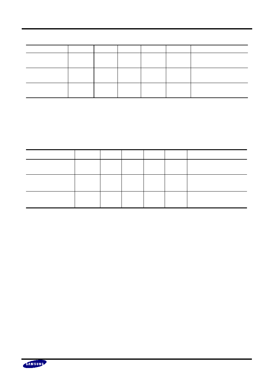
ABSOLUTE MAXIMUM RATINGS
Characteristics
Symbol
Value
Unit
Supply Voltage
VDD
3.3
V
Analog Input Voltage
AINT/AINC
VSS to VDD
V
Digital Input Voltage
CLK
VSS to VDD
V
Reference Voltage
REFTOP/REFBOT/
REFTOP1/REFBOT1
VSS to VDD
V
Storage Temperature Range
Tstg
-40 to 125
ļC
Operating Temperature Range
Topr
0 to 70
ļC
NOTES
1. Absolute maximum rating specifies the values beyond which the device may be damaged permanently. Exposure to
ABSOLUTE MAXIMUM RATING conditions for extended periods may affect reliability. Each condition value is
applied with the other values kept within the following operating conditions and function operation under any of
these conditions is not implied.
2. All voltages are measured with respect to VSS unless otherwise specified.
3. 100pF capacitor is discharged through a 1.5Kohm resistor (Human body model)
RECOMENDED OPERATING CONDITIONS
Characteristics
Symbol
Min
Typ
Max
Unit
Supply Voltage
VDD25A1
VDD25A2
VDD25A3
2.3
2.5
2.7
V
Reference Input Voltage
REFTOP
REFBOT
1.75
0.75
V
Analog Input Voltage
AINT
AINC
Ī
1
(differential)
V
Operating Temperature
Toper
0
-
70
ļC
NOTES
It is strongly recommended that all the supply pins (VDD25A1, VDD25A2, VDD25A3) be powered from the same
source to avoid power latch-up.
3/12
SEC ASIC
ADC1256X
12BIT 20MSPS ADC
ANALOG
DC ELECTRICAL CHARACTERISTICS
Characteristics
Symbol
Min
Typ
Max
Unit
Test Condition
Differential
Nonlinearity
DNL
-
Ī
0.8
Ī
1
LSB
REFTOP=1.75V
REFBOT=0.75V
Integral
Nonlinearity
INL
-
Ī
1.2
Ī
3
LSB
REFTOP=1.75V
REFBOT=0.75V
Offset
Voltage
OFF
-
10
15
mV
REFTOP=1.75V
REFBOT=0.75V
(Converter Specifications : VDD25A1=VDD25A2=VDD25A3=2.5V, VSS25A1=VSS25A2=VSS25A3=0V,
Toper=25ļC, REFTOP=1.75V, REFBOT=0.75V unless otherwise specified)
AC ELECTRICAL CHARACTERISTICS
Characteristics
Symbol
Min
Typ
Max
Unit
Test Condition
Maximum
Conversion Rate
fc
-
-
20
MHz
AIN=AINT-AINC
Dynamic Supply
Current
IVDD
-
46
60
mA
fc=20MHz
(without system load)
Signal-to-Noise &
Distortion Ratio
SNDR
56
62
-
dB
AIN=1MHz
(Conversion Specifications : VDD25A1=VDD25A2=VDD25A3=2.5V, VSS25A1=VSS25A2=VSS25A3=0V,
Toper=25ļC, REFTOP=1.75V, REFBOT=0.75V unless otherwise specified)
4/12
SEC ASIC
ADC1256X
12BIT 20MSPS ADC
ANALOG
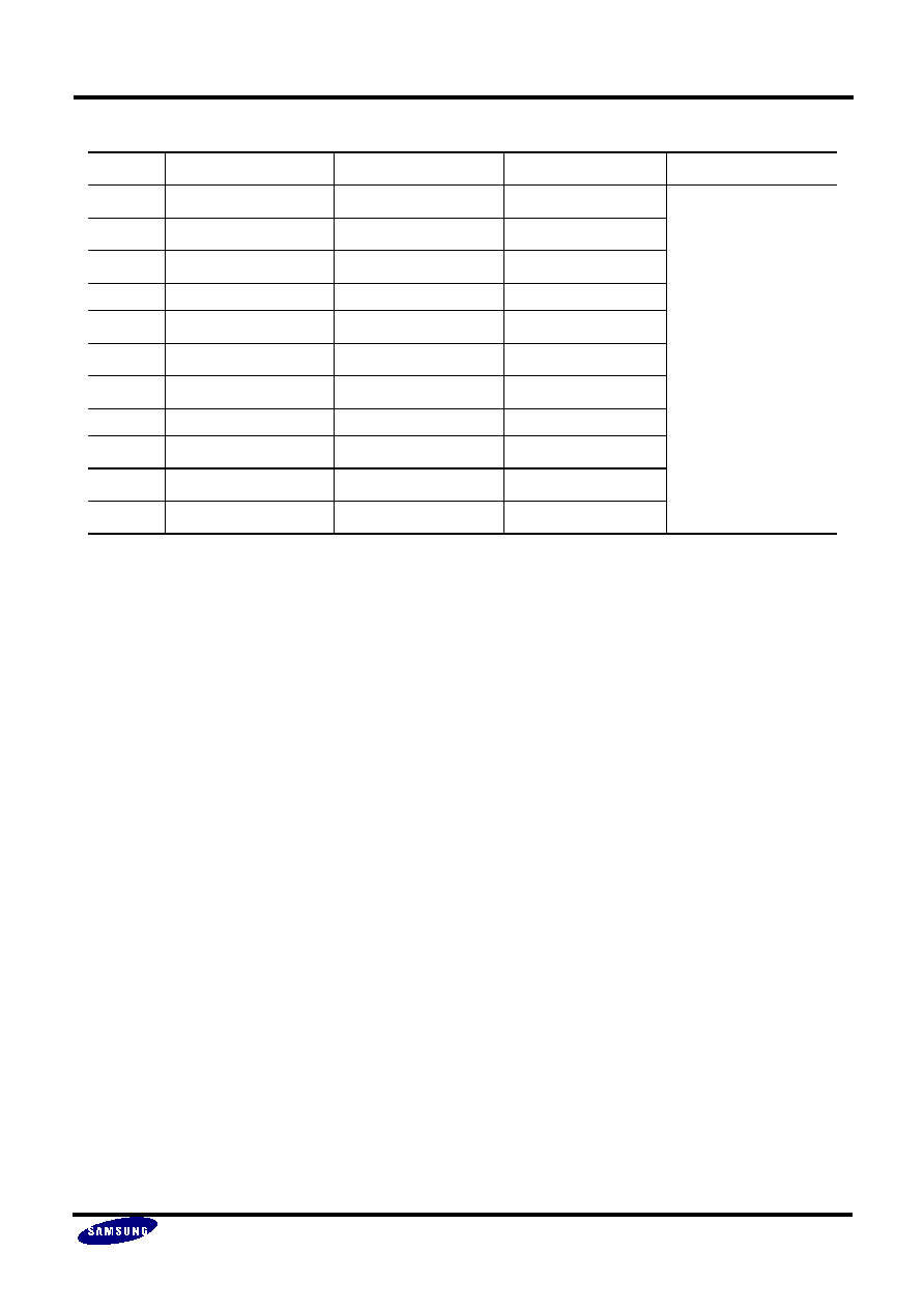
I/O CHART
Index
AINT Input (V)
AINC Input (v)
Digital Output
0
0.2500 ~ 0.2505
1.25
0000 0000 0000
1LSB=0.488mV
REFTOP=1.75V
REFBOT=0.75V
1
0.2505 ~ 0.2510
1.25
0000 0000 0001
2
0.2510 ~ 0.2515
1.25
0000 0000 0010
~
~
~
~
2047
1.2495 ~ 1.2500
1.25
0111 1111 1111
2048
1.2500 ~ 1.2505
1.25
1000 0000 0000
2049
1.2505 ~ 1.2510
1.25
1000 0000 0001
~
~
~
~
4093
2.2485 ~ 2.2490
1.25
1111 1111 1101
4094
2.2490 ~ 2.2495
1.25
1111 1111 1110
4095
2.2495 ~ 2.2500
1.25
1111 1111 1111
5/12

SEC ASIC
ADC1256X
12BIT 20MSPS ADC
ANALOG
TIMING DIAGRAM
A1
A2
D1
D2
D3 D4
D5
A5
AINT
CKIN
DO[11:0]
Input sampling period
6/12

SEC ASIC
ADC1256X
12BIT 20MSPS ADC
ANALOG
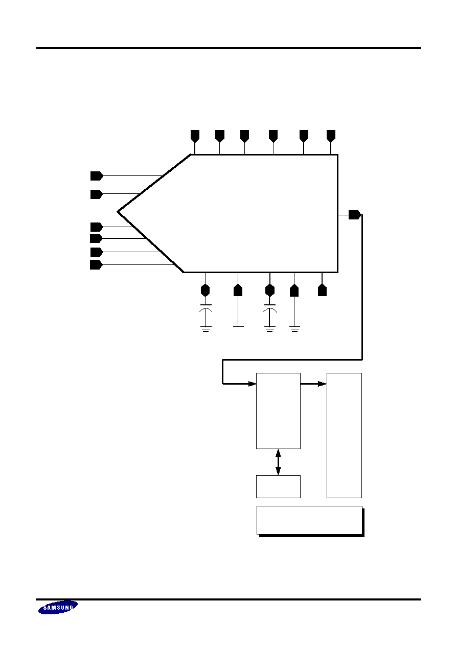
FUNCTIONAL DESCRIPTION
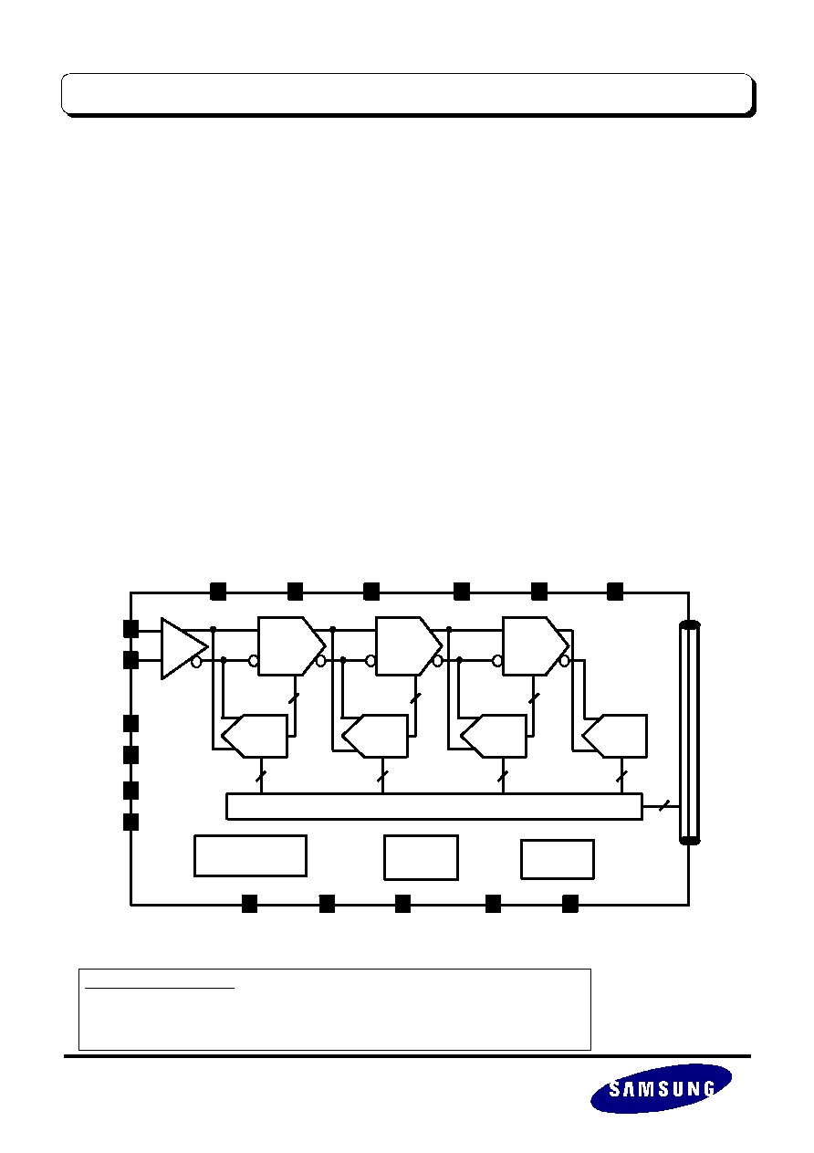
1. The ADC1256X is a CMOS four step pipelined
Analog-to-Digital Converter. It contains four 4-bit
flash A/D Converters and three multiplying D/A
Conveters. The 4-bit flash ADC is composed of
2
4
-1 latching comparators, and multiplying DAC is
composed
of
2◊(2
4
+1)
capacitors
and
two
fully-differential amplifiers.
2. The ADC1256X operates as follows. During the
first "L" cycle of external clock the analog input
data is sampled, and the input is held from the
rising edge of the external clock, which is fed to
the first 4-bit flash ADC, and the first multiplying
DAC. Multiplying DAC reconstructs a voltage
corresponding to the first 4-bit ADC's output, and
finally amplifies a residue voltage by 2
3
. The
second and third 4-bit flash ADC, and MDAC are
worked as same manner. Finally amplified residue
voltage at the third multiplying DAC is fed to the
last 4-bit flash ADC decides final 4-bit digital code.
3. ADC1256X has the error correction scheme, which
handles the output from mismatch in the first,
second, third and fourth flash ADC.
MAIN BLOCK DESCRIPTION
1. SHA
SHA (Sample-and-Hold Amplifier) is the circuit that
samples the analog input signal and hold that value
until next sample-time. It is good as small as its
different value between analog input signal and
output signal. SHA amp gain is higher than 70dB
at 20MHz conversion rate, its settling-time must be
shorten than 18ns with less than 1/2 LSB error
voltage at 12bit resolution. This SHA is consist of
fully differential op amp, switching tr. and sampling
capacitor. The sampling clock is non-overlapping
clock (Q1, Q2) and sampling capacitor value is
about 3.0pF. SHA uses independent bias to protect
interruption of any other circuit. SHA amp is
designed that open-loop dc gain is higher than
70dB, phase margin is higher than 60 degrees. Its
input block is designed to be the rail-to-rail
architecture using complementary different pair.
2. FLASH
The 4-bit flash converters compare analog signal
(TAH output) with reference voltage, and that
results transfer to MDAC and digital correction
logic
block.
It
is
realized
fully
differential
comparators
of
15EA.
Considering
self-offset,
dynamic feed through error, it should distinguish
40mV at least. First, the comparators charge the
reference voltage at the sampling capacitors before
transferred SHA output.That operation is performed
on the phase of Q2, and discharging on the phase
of Q1. That is, the comparators compare relative
different values dual input voltage with dual
reference voltage. Its output during Q1 operation is
stored at the pre-latch block by Q1P.
3. MDAC
MDAC is the most important block at this ADC
and it decides the characteristics. MDAC is consist
of two stage op amp, selection logic and capacitor
array (c_array). c_array's compositions are the
capacitors to charge the analog input and and the
reference voltage, switches to control the path.
Selection logic controls the c_array internal switches
. If Q1 is high, selection's output are all low, the
switches of tsw1 are off, the switches of tsw2 are
all on. Therefore the capacitors of c_array can
charge analog input values held at SHA.
7/12
SEC ASIC
ADC1256X
12BIT 20MSPS ADC
ANALOG
CORE EVALUATION GUIDE
1. ADC function is evaluated by external check on the bidirectional pads connected to input nodes of HOST DSP
back-end circuit.
2. The reference voltages may be biased internally through resistor divider.
D[11:0]
Digital Mux
Bidirectional
PAD
HOST
DSP
CORE
D[11:0]
D[11:0]
(ADC Function Test &
externally forced Digital Input)
adc1256x
AINC
ITEST STBY
CKIN
AINT
REFTOP1
REFTOP
REFBOT
REFBOT1
SPEEDUP
CML
VDD25A1
VSS25A1 VBBA1 VDD25A2
VSS25A2
VBBA2
DO[11:0]
[MSB:LSB]
vdd
8/12
SEC ASIC
ADC1256X
12BIT 20MSPS ADC
ANALOG
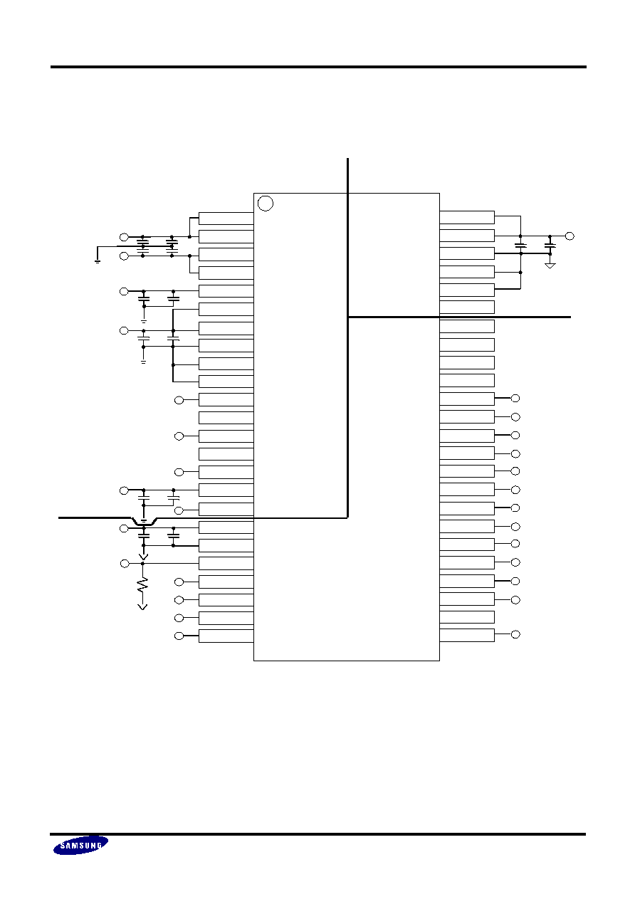
PACKAGE CONFIGURATION
NOTES
1. NC denotes "No Connection".
Digital II
Analog
ADC1256X
1
2
3
4
5
6
7
8
9
10
11
12
13
14
15
16
17
18
19
20
21
22
23
24
48
47
46
45
44
43
42
41
40
39
38
37
36
35
34
33
32
31
30
29
28
27
26
25
REFTOP1
REFTOP
REFBOT
REFBOT1
CML
VDD25A1
VDD25A1
VBBA1
VSS25A1
VSS25A1
AINT
NC
AINC
NC
SPEEDUP
ITEST
STBY
VDD25A3
VSS25A3
CKIN
TEST1
TEST2
NC
NC
VDD25A2
VDD25A2
VSS25A2
VSS25A2
VBBA2
NC
NC
NC
NC
NC
DO[11]
DO[10]
DO[9]
DO[8]
DO[7]
DO[6]
DO[5]
DO[4]
DO[3]
DO[2]
DO[1]
DO[0]
NC
TRIST
50ohm
10u
0.1u
0.1u
10u
0.1u
10u
0.1u
10u
10u
0.1u
0.1u
10u
0.1u
10u
Digital I
9/12

SEC ASIC
ADC1256X
12BIT 20MSPS ADC
ANALOG
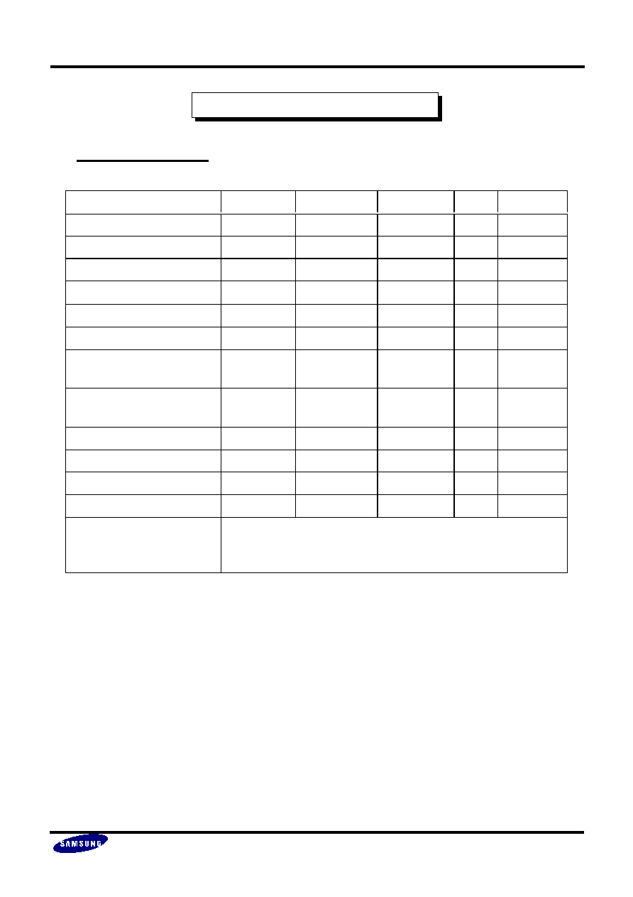
PACKAGE PIN DESCRIPTION
NOTES
1. I/O TYPE PP and PG denote PAD Power and PAD Ground respectively
No.
NAME
I/O
TYPE
PIN DESCRIPTION
CONFIGURATION
1
REFTOP1
AI
Reference Top Sence (1.75V)
2
REFTOP
AI
Reference Top Force (1.75V)
3
REFBOT
AI
Reference bottom Force (0.75V)
4
REFBOT1
AI
Reference bottom Sense (0.75V)
5
CML
AB
Common Mode Level (Test Pin)
6, 7
VDD25A1
AP
Analog Power (2.5V)
8
VBBA1
AG
Analog Sub Bias
9, 10
VSS25A1
AG
Analog Ground
11
AINT
AI
Analog Input +
13
AINC
AI
Analog Input -
15
SPEEDUP
DI
VDD=Normal (
20MHz)
GND=Speed Down (
15MHz)
16
ITEST
AB
open=use internal bias circuit
17
STBY
DI
VDD=Power saving (Standby),
GND=Normal
18
VDD25A3
PP
PAD Power (2.5V)
19
VSS25A3
PG
PAD Ground
20
CKIN
DI
Sampling Clock Input
21
TEST1
AO
Monitoring (TEST) Cell Pin1,
GND=Normal
22
TEST2
AO
Monitoring (TEST) Cell Pin2,
GND=Normal
25
TRIST
DI
Tristate Buffer Input
VDD=High Impedance,
GND=Normal
27
DO[0]
DO
Digital Output (LSB)
28~37
DO[1:10]
DO
Digital Output
38
DO[11]
DO
Digital Output (MSB)
44
VBBA2
DG
Digital Sub Bias
45, 46 VSS25A2
DG
Digital GND
47, 48 VDD25A2
DP
Digital Power (2.5V)
REFTOP
VBBA1
TEST1
TEST2
NC
NC
ADC1256X
1
2
3
4
5
6
7
8
9
10
11
12
13
14
15
16
17
18
19
20
21
22
23
24
48
47
46
45
44
43
42
41
40
39
38
37
36
35
34
33
32
31
30
29
28
27
26
25
REFTOP1
REFBOT
CML
VDD25A1
VDD25A1
VSS25A1
VSS25A1
AINT
NC
AINC
NC
SPEEDUP
ITEST
STBY
VDD25A3
VSS25A3
CKIN
VDD25A2
VDD25A2
VSS25A2
VSS25A2
VBBA2
NC
NC
NC
NC
NC
DO[11]
DO[10]
DO[9]
DO[8]
DO[7]
DO[6]
DO[5]
DO[4]
DO[3]
DO[2]
DO[1]
DO[0]
NC
TRIST
REFBOT1
10/12

SEC ASIC
ADC1256X
12BIT 20MSPS ADC
ANALOG
USER GUIDE
1. Input Range
- If you want to using the single-ended input, you should use he input range as below.
AINT : 0.25V ~ 2.25V,
AINC : 1.25V.
- If you want to using the differential input, you should use the input range as below.
AINT : 0.75V ~ 1.25V,
AINC : 0.75V ~ 1.25V.
AIN : AINT-AINC
2. Speed Up
The initial target speed of ADC1256X is 20MHz.
If you want speed down (about 15MHz), you should connect the SPEEDUP port to 'LOW'.
And it can save the total power consumption about 10 ~ 15%.
3. Power Consumption Optimization
Yon can optimize the power consumption, as control the ITEST voltage level precisely .
11/12
SEC ASIC
ADC1256X
12BIT 20MSPS ADC
ANALOG
FEEDBACK REQUEST
ADC Specification
Parameter
Min
Typ
Max
Unit
Remarks
Supply voltage
V
Reference Input voltage
V
Analog Input voltage
Vpp
Operating temperature
ļC
Integral non-linearity error
LSB
Differential non-linearity error
LSB
Offset voltage error
(Bottom)
mV
Offset voltage error
(Top)
mV
Maximum conversion rate
MSPS
Dynamic supply current
mA
Power dissipation
mW
Signal-to-noise ratio
dB
Digital output format
(Provide detailed description
& timing diagram)
- What do you want to choose as power supply voltages?
- What resolution do you need for ADC?
- How about conversion speed(data in
data out)?
- How many cycles do exist during the latency of ADC (pipelined delay)?
- What's the input range? And then what do you need between single input and differential input?
- Could you explain external/internal pin configurations as required?
Specially requested function list :
12/12