 | –≠–ª–µ–∫—Ç—Ä–æ–Ω–Ω—ã–π –∫–æ–º–ø–æ–Ω–µ–Ω—Ç: bw0405xb | –°–∫–∞—á–∞—Ç—å:  PDF PDF  ZIP ZIP |

0.35
µ
µ
µ
µ
m 16-BIT 44.1KHZ SIGMA-DELTA STEREO DAC
BW0405XB
1
GENERAL DESCRIPTION
This product is SD Digital-To-Analog Converter for digital audio System (CDP). The product contains Serial-to-
Parallel Converter and Compensation Filter, Digital Volume Attenuator by the MICOM Interface, De-Emphasis
Filter, FIR filter, Sinc Filter, digital sigma-delta modulator, analog postfilter, AIF (Anti-Image-Filter). The normal
input and output channels provides 95dB SNR (Signal to Noise Ratio) over in band (20kHz).
The product employs the 1bit 4th-order sigma-delta architecture with 16bit resolution, over sampling of 64X. And
analog postfilter with low clock sensitivity and linear phase, filters the shaping-nosie and outputs analog voltage
with high resolution. An on-chip reference voltage is included to allow single supply operations.
FEATURES
-- 16bit SD Digital-To-Analog Converter
-- On-Chip Analog Postfilter
-- Filtered Line-Level Outputs, Linear Phase Filtering
-- On-Chip Voltage Reference
-- 90dB SNR
-- Sampling Rate 32KHz/44.1kHz/48KHz
-- Input Rate 1Fs or 2Fs by Normal Mode/Double Mode Selection
-- Zero Input Detection Mute
-- On-Chip Compensation Filter
-- Input Volume Attenuator by the MICOM Interface
-- On-Chip De-Emphasis Filter
(32KHz/44.1KHz/48KHz)
-- On-Chip 4 times oversampling Digital Filter
-- Low Clock Jitter Sensitivity
-- Single 3.3V ~ 2.5V Power Supply
APPLICATIONS
CD Player, Portable CD Player, CD-ROM, Video-CD, Mini-Disk, DVD etc
BW0405XB
0.35
µ
µ
µ
µ
m 16-BIT 44.1KHZ SIGMA-DELTA STEREO DAC
2
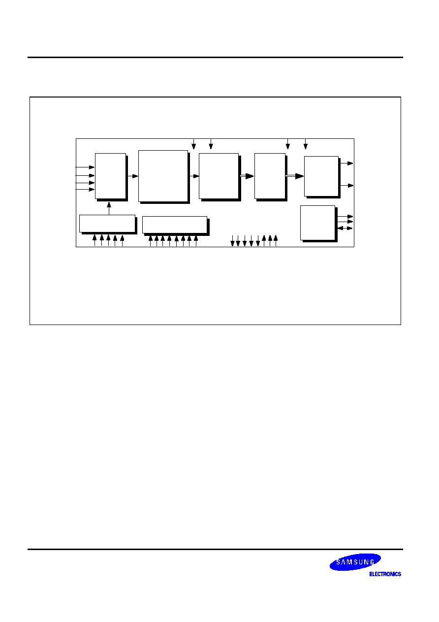
FUNCTIONAL BLOCK DIAGRAM
DAC
&
Analog
Postfilter
Sinc Filter
&
Sigma-Delta
Modulator
Compensation
Filter
&
De-emphsis
&
FIR Filter
Anti-Imaging
Filter
Timing Generation
Voltage
Reference
S/P
Converter
&
Attenuator
SDATA
BCK
LRCK
ZDENL
AOUTL
VREF
VHALF
IREF
AOUTR
I
D
N
U
M
<
7
:
0
>
F
S
E
L
<
1
:
0
>
M
L
D
M
D
A
T
A
M
C
L
K
MICOM Interface
D
E
E
M
D
N
M
S
C
K
R
S
T
B
B
I
S
T
O
N
P
M
U
T
E
L
P
D
L
T
S
E
L
I
A
D
S
R
I
A
D
S
L
I
F
S
6
4
O
D
S
R
O
D
S
L
O
F
S
6
4
S
D
I
A
G
S
E
R
R
O
R
B
VDDD VSSD
VDDA VSSA

0.35
µ
µ
µ
µ
m 16-BIT 44.1KHZ SIGMA-DELTA STEREO DAC
BW0405XB
3
EMBEDDED CORE BLOCK DIAGRAM
MSCK
BCK
LRCK
SDATA
AOUTL
VHALF
AOUTR
ZDENL
DEEM
DN
MUTEL
PDL
RSTB
V
S
S
A
V
D
D
A
V
D
D
D
V
S
S
D
Audio Processor
(DSP)
bw0405xb
SDIAG
SERRORB
OFS64
ODSL
ODSR
BISTONP
TSEL
IFS64
IADSL
IADSR
MUX_SEL
External
Inputs
These are test pins for internal blocks of the core.
So you don't need the internal test mode.
Make the test control pins disable ('L') state and
Output and bidirectional pins leave foalting.
MCLK
MLD
MDATA
FSEL<1:0>
IDNUM<7:0>
M
U
X
4
4
4
IREF
VSSD
6
13
5
External
VREF
EMBEDDED CORE USER GUIDE
-- Digital serial data input and clock input refer to digital input format.
-- Digital control pins inform refer to pin description.
-- Micom I/F pin inform refer to micom interface. IDNUM<7:0> are ID number setting pins for micom Interface.
-- External application of analog output pins refer to application circuit.
-- If you want to test only embedded analog core block (Sigma-Delta DAC), you can do it just adding the 4 pins to
supply digital serial input data (LRCK, BCK, SDATA, MSCK) and MUX block.
-- Analog power (VDDA,VSSA) and digital power (VDDD, VSSD) should be seperated.
-- VBB pin should be connected to analog ground.
-- Two pads should be dedicated to analog power (VDDA, VSSA)
-- If you need not use test mode for the testability of internal core block, you make internal core block test pins
disable state. (Test Input pins are 'L' state and Test output, bidirection pins leave floating)
BW0405XB
0.35
µ
µ
µ
µ
m 16-BIT 44.1KHZ SIGMA-DELTA STEREO DAC
4
CORE PIN DESCRIPTION
Symbol
I/O
Type
I/O
Pad
Description
Power
Supply
Pins
VDDD
DP
vdd3t_bb
Digital
Supply
VSSD
DG
vsst_bb
Digital
Ground
VDDA
AP
vdd3t_bb
Analog
Supply
VSSA
AG
vsst_bb
Analog
Ground
Digital
Pins
MSCK
DI
picc_bb
Master
Clock
Input.
384Fs
Clock
BCK
DI
picc_bb
Bit
Clock
Input.
(32Fs
or
64Fs)
LRCK
DI
picc_bb
Sample
Rate
Clock
Input.
(Fs
or
2Fs)
SDATA
DI
picc_bb
Serial
Digital
Input
MCLK
DI
picc_bb
Micom
Interface
Clock
Input
MLD
DI
picc_bb
Micom
Interface
Command
load
Input
(When
low,load)
MDATA
DI
picc_bb
Micom
Interface
Command
Data
Input
DEEM
DI
picc_bb
De-Emphasis
On/Off.
"H"
is
enabled.
"L"
is
disabled.
DN
DI
picc_bb
Input
Rate
Select.
High
is
Double(2Fs)
Mode,
Low
is
Normal(Fs)
Mode.
MUTEL
DI
picc_bb
Analog
Output
Mute.
"L"
enabled
ZDENL
DI
picc_bb
Zero Input Detection Enable. "L" is enabled. "H" is disabled
FSEL<1:0>
DI
picc_bb
De-Emphasis Sampling Frequency Mode Select
FSEL<1:0> Sampling Frequency
H H 48KHz
H L 32KHz
L H 48KHz
L L 44.1KHz
IDNUM<7:0>
DI
picc_bb
Micom Interface ID Number setting Input
PDL
DI
picc_bb
Power
Down.
"L"
enabled
RSTB
DI
picc_bb
Reset
Input.
"L"
Enabled
Analog
Pins
AOUTL
AO
poa_bb
Analog
Output
for
L-CH
AOUTR
AO
poa_bb
Analog
Output
for
R-CH
VHALF
AO
poar50_bb Reference
Voltage
Output
for
Bypass
VREF
AO
poar50_bb Reference Voltage Output for Bypass
Core
Internal
Block
Test
Pins
0.35
µ
µ
µ
µ
m 16-BIT 44.1KHZ SIGMA-DELTA STEREO DAC
BW0405XB
5
CORE PIN DESCRIPTION (Continued)
Symbol
I/O
Type
I/O
Pad
Description
BISTONP
DI
picc_bb
Memory
Bist
Test
Mode.
"H"
enabled
TSEL
DI
picc_bb
Test
pin
for
Analog
Postfilter
Input
Selection
IFS64
DI
picc_bb
64X
Sampling
Clock
Input
for
Analog
Postfilter
(When
TSEL=H)
IADSL
DI
picc_bb
Inputs
for
Analog
Postfilter
of
L-CH
(When
TSEL=H)
IADSR
DI
picc_bb
Inputs
for
Analog
Postfilter
of
R-CH
(When
TSEL=H)
SDIAG
DO
pot2_bb
Test
Output
pin
for
embeded
memory
BIST
(BIST_ON="H")
SERRORB
DO
pot2_bb
Test
Output
Pin
for
Embeded
memory
BIST
(BIST_ON="H")
OFS64
DO
pot2_bb
64X
Sampling
Clock
output
for
Digital
sigma-delta
Modulator
ODSL
DO
pot2_bb
L-CH
Output
for
Digital
sigma-delta
Modulator.
ODSR
DO
pot2_bb
R-CH
Output
for
Digital
sigma-delta
Modulator.
IREF
AB
poa_bb
Test
Pin
for
Analog
Supply
Current
I/O Type Abbr.
-- AI: Analog Input
-- DI: Digital Input
-- AO: Analog Output
-- DO: Digital Output
-- AB: Analog Bidirectional
-- DB: Digital Bidirectional
-- AP: Analog Power
-- DP: Digital Power
-- AG: Analog Ground
-- DG: Digital Ground

BW0405XB
0.35
µ
µ
µ
µ
m 16-BIT 44.1KHZ SIGMA-DELTA STEREO DAC
6
CORE CONFIGURTION
bw0405xb
Used Power:
(VDDD VSSD VDDA VSSA)
MSCK
BCK
LRCK
SDATA
ZDENL
MCLK
MLD
MDATA
FSEL<1:0>
IDNUM<7:0>
DEEM
DN
MUTEL
PDL
RSTB
BISTONP
TSEL
IFS64
IADSL
IADSR
AOUTL
AOUTR
VHALF
VREF
IREF
SDIAG
SERRORB
OFS64
ODSL
ODSR
ABSOLUTE MAXIMUM RATINGS
Characteristics
Symbol
Values
Unit
Supply Voltage
VDDD,VDDA
-0.15 ~ 3.8
V
Voltage on Any Digital Pin
Vin
VSSD-0.15 to VDDD+0.15
V
Storage Temperature Range
Tstg
-45 to +125
∞
C
RECOMMENDED OPERATING CONDITIONS
Charateristics
SYMBOL
MIN
TYP
MAX
UNITS
Supply Voltage
VDDD
VDDA
2.3
2.5
3.6
V
Operating Temp.
Topr
0
25
70
∞
C

0.35
µ
µ
µ
µ
m 16-BIT 44.1KHZ SIGMA-DELTA STEREO DAC
BW0405XB
7
ELECTRICAL CHARACTERISTICS
(VDDD,VDDA=2.5V, Temp=25
∞
C, Fs=44.1kHz, Signal Frequency=20-20kHz, Cload of AoutL, AoutR=10pF)
Parameter
Min
Typ
Max
Units
Resolution
16
bits
SNR
<1>
80
90
dB
THD
<2>
0.005
0.01
%
SND(THD+Noise)
<3>
76
80
dB
Dynamic Range
<4>
85
90
dB
Reference Voltage Ouput
0.5 x VDDA
V
Frequency Responce
±
0.1
±
0.5
dB
Analog Output
Voltage Range
0.75 x VDDA
Vpp
Load Impedance
10k
Digital Filter
Pass Band Ripple
±
0.0072
dB
Stop Band Attenuation
62.7
dB
Pass Band
0.45
Fs
Power Supply
Analog Current
2
3
mA
Digital Current
5
6
mA
Power Dissipation
17.5
22.5
mW
Power Down Current
0.1
1
mA
NOTES:
1.
1kHz 0dB Sinewave Input, EIAJ
2.
1kHz -3dB Sinewave Input
3.
1kHz 0dB Sinewave Input, (Not EIAJ)
4.
1kHz -60dB Sinewve Input, and then measured data + 60dB

BW0405XB
0.35
µ
µ
µ
µ
m 16-BIT 44.1KHZ SIGMA-DELTA STEREO DAC
8
AC TIMING CHARACTERISTICS
(VDDD=2.5V, VSSD=0V, Temp=25
∞
C)
Characteristics
Symbol
Min
Typ
Max
Unit
MSCK Frequency
Fmck
≠
16.9344
≠
MHz
BCK Frequency (Normal/Doube Mode)
Fbck
1.4112 / 2.8224
(Normal / Double)
≠
MHz
MSCK Rising and LRCK Edge Dealay
Tmld
10
≠
≠
ns
MSCK Risng and LRCK Edge Setup Time
Tmlst
10
≠
≠
ns
BCK Rising and LRCK Edge Dealay
Tbld
10
≠
≠
ns
BCK Risng and LRCK Edge Setup Time
Tblst
10
≠
≠
ns
SDATA and BCK Rising Setup Time
Tsbst
10
≠
≠
ns
BCK Ring and SDATA Hold Time
Tbsht
10
≠
≠
ns
1/Fbck
0.5 VDDD
MSCK
BCK
0.5 VDDD
1/Fmck
LRCK
0.5 VDDD
0.5 VDDD
Tmld
Tmlst
MSCK
SDATA
0.5 VDDD
LRCK
0.5 VDDD
0.5 VDDD
Tbld
Tblst
Tsbst
Tbsht
BCK
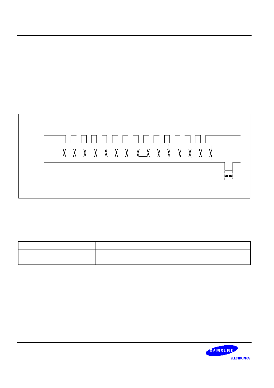
Figure 1. Timing Chart
0.35
µ
µ
µ
µ
m 16-BIT 44.1KHZ SIGMA-DELTA STEREO DAC
BW0405XB
9
CLOCK INPUT AND SERIAL INPUT DATA INFORM (FS=44.1KHZ)
DN is normal and double mode selection control pin. Refer to the following table for clock input inform.
Table 1. Input Clock Informs
Normal
Mode
(DN='Low')
Double
Mode
(DN='High')
LRCK
44.1kHz
88.2kHz
MSCK
16.9344MHz
16.9344MHz
BCK
1.4112MHz
2.8224MHz
Serial input data (SDATA) is MSB fisrt at falling edge triggered of BCK.
LSB
LRCK
BCK
SDATA
R-CH DATA
L-CH DATA
MSB
LSB+1
LSB+2
MSB-1 MSB-2
...
LSB
MSB
LSB+1
LSB+2
MSB-1 MSB-2
...
...
...
...
...
Figure 2. Digital Input Data Format
BW0405XB
0.35
µ
µ
µ
µ
m 16-BIT 44.1KHZ SIGMA-DELTA STEREO DAC
10
MICOM INTERFACE (DIGITAL ATTENUATION)
This
product
can
do
the
function
of
digital
attenuation
whenever
it
receives
thd
MDATA,
MLD,
MCLK
signals
form
the
MICOM.
When
the
14-bit
serial
data
is
applied
to
the
MDATA,
MCLK,
MLD
in
the
form
of
Fig3,
according
to
the
data
digital
attenuation
is
accomplished.
The
lower
eight
LSBs
should
be
5D(LSB
First
Format-Hex)
and
according
to
the
upper
6
bits(LSB
First
Format-Bin)
the
attenuation
level
can
be
adjusted.
(see
Table1)
When
RSTB
is
low
state
the
latch
circuitry
for
setting
the
attenuation
level
becomes
reset
and
the
attenuation
level
is
0dB.
At
this
instance,
because
the
digital
filter
circuit
gets
to
stop
operation
the
act
of
attenuation
is
impossible.
In
addition,
whenever
MDATA
is
not
carried,
MCLK
must
be
'HIGH'
state.
In
case
of
no
attenuation
fuction
needed,
MDATA
should
be
'L',
MCLK
and
MLD
should
be
'H.
M2
M3
M4
M5
Don't
Care
MCLK
MDATA
MLD
M1
M0
Don't
Care
Over 550ns needed
MSB
LSB
MSB
LSB
ID0
ID1
ID2
ID3
ID4
ID5
ID6
ID7
Figure 3. MICOM Interface Timing Chart
FSEL<1:0> is de-emphasis sampling frequency mode selection control pin. Refer to the following table for function
inform.
Table 2. De-Emphasis Sampling Frequency Mode Selection
FSEL<1>°¨ FSEL<0>
"High"
"Low"
"High"
48kHz
32kHz
"Low"
48KHz
44.1KHz
0.35
µ
µ
µ
µ
m 16-BIT 44.1KHZ SIGMA-DELTA STEREO DAC
BW0405XB
11
Table 3. Digital Attenuation Level
MDATA
Attenuation
MDATA
Attenuation
MSB ~ LSB MSB ~ LSB
ID7 ~ ID0 M5 M4 M3 M2 M1 M0
Level (dB)
MSB ~ LSB MSB ~ LSB
ID7 ~ ID0 M5 M4 M3 M2 M1 M0
Level (dB)
IDNUM<7:0> 0 0 0 0 0 0
IDNUM<7:0> 0 0 0 0 0 1
IDNUM<7:0> 0 0 0 0 1 0
IDNUM<7:0> 0 0 0 0 1 1
0
-0.28
-0.42
-0.56
IDNUN<7:0> 1 0 0 0 0 0
IDNUN<7:0> 1 0 0 0 0 1
IDNUN<7:0> 1 0 0 0 1 0
IDNUN<7:0> 1 0 0 0 1 1
-6.30
-6.58
-6.88
-7.18
IDNUN<7:0> 0 0 0 1 0 0
IDNUN<7:0> 0 0 0 1 0 1
IDNUN<7:0> 0 0 0 1 1 0
IDNUN<7:0> 0 0 0 1 1 1
-0.71
-0.86
-1.01
-1.16
IDNUN<7:0> 1 0 0 1 0 0
IDNUN<7:0> 1 0 0 1 0 1
IDNUN<7:0> 1 0 0 1 1 0
IDNUN<7:0> 1 0 0 1 1 1
-7.50
-7.82
-8.16
-8.52
IDNUN<7:0> 0 0 1 0 0 0
IDNUN<7:0> 0 0 1 0 0 1
IDNUN<7:0> 0 0 1 0 1 0
IDNUN<7:0> 0 0 1 0 1 1
-1.32
-1.48
-1.64
-1.80
IDNUN<7:0> 1 0 1 0 0 0
IDNUN<7:0> 1 0 1 0 0 1
IDNUN<7:0> 1 0 1 0 1 0
IDNUN<7:0> 1 0 1 0 1 1
-8.89
-9.28
-9.68
-10.10
IDNUN<7:0> 0 0 1 1 0 0
IDNUN<7:0> 0 0 1 1 0 1
IDNUN<7:0> 0 0 1 1 1 0
IDNUN<7:0> 0 0 1 1 1 1
-1.97
-2.14
-2.32
-2.50
IDNUN<7:0> 1 0 1 1 0 0
IDNUN<7:0> 1 0 1 1 0 1
IDNUN<7:0> 1 0 1 1 1 0
IDNUN<7:0> 1 0 1 1 1 1
-10.55
-11.02
-11.51
-12.04
IDNUN<7:0> 0 1 0 0 0 0
IDNUN<7:0> 0 1 0 0 0 1
IDNUN<7:0> 0 1 0 0 1 0
IDNUN<7:0> 0 1 0 0 1 1
-2.68
-2.87
-3.06
-3.25
IDNUN<7:0> 1 1 0 0 0 0
IDNUN<7:0> 1 1 0 0 0 1
IDNUN<7:0> 1 1 0 0 1 0
IDNUN<7:0> 1 1 0 0 1 1
-12.60
-13.20
-13.84
-14.54
IDNUN<7:0> 0 1 0 1 0 0
IDNUN<7:0> 0 1 0 1 0 1
IDNUN<7:0> 0 1 0 1 1 0
IDNUN<7:0> 0 1 0 1 1 1
-3.45
-3.66
-3.87
-4.08
IDNUN<7:0> 1 1 0 1 0 0
IDNUN<7:0> 1 1 0 1 0 1
IDNUN<7:0> 1 1 0 1 1 0
IDNUN<7:0> 1 1 0 1 1 1
-15.30
-16.12
-17.04
-18.06
IDNUN<7:0> 0 1 1 0 0 0
IDNUN<7:0> 0 1 1 0 0 1
IDNUN<7:0> 0 1 1 0 1 0
IDNUN<7:0> 0 1 1 0 1 1
-4.30
-4.53
-4.76
-5.00
IDNUN<7:0> 1 1 1 0 0 0
IDNUN<7:0> 1 1 1 0 0 1
IDNUN<7:0> 1 1 1 0 1 0
IDNUN<7:0> 1 1 1 0 1 1
-19.22
-20.56
-22.14
-24.08
IDNUN<7:0> 0 1 1 1 0 0
IDNUN<7:0> 0 1 1 1 0 1
IDNUN<7:0> 0 1 1 1 1 0
IDNUN<7:0> 0 1 1 1 1 1
-5.24
-5.49
-5.75
-6.02
IDNUN<7:0> 1 1 1 1 0 0
IDNUN<7:0> 1 1 1 1 0 1
IDNUN<7:0> 1 1 1 1 1 0
IDNUN<7:0> 1 1 1 1 1 1
-26.58
-30.10
-36.12
-
BW0405XB
0.35
µ
µ
µ
µ
m 16-BIT 44.1KHZ SIGMA-DELTA STEREO DAC
12
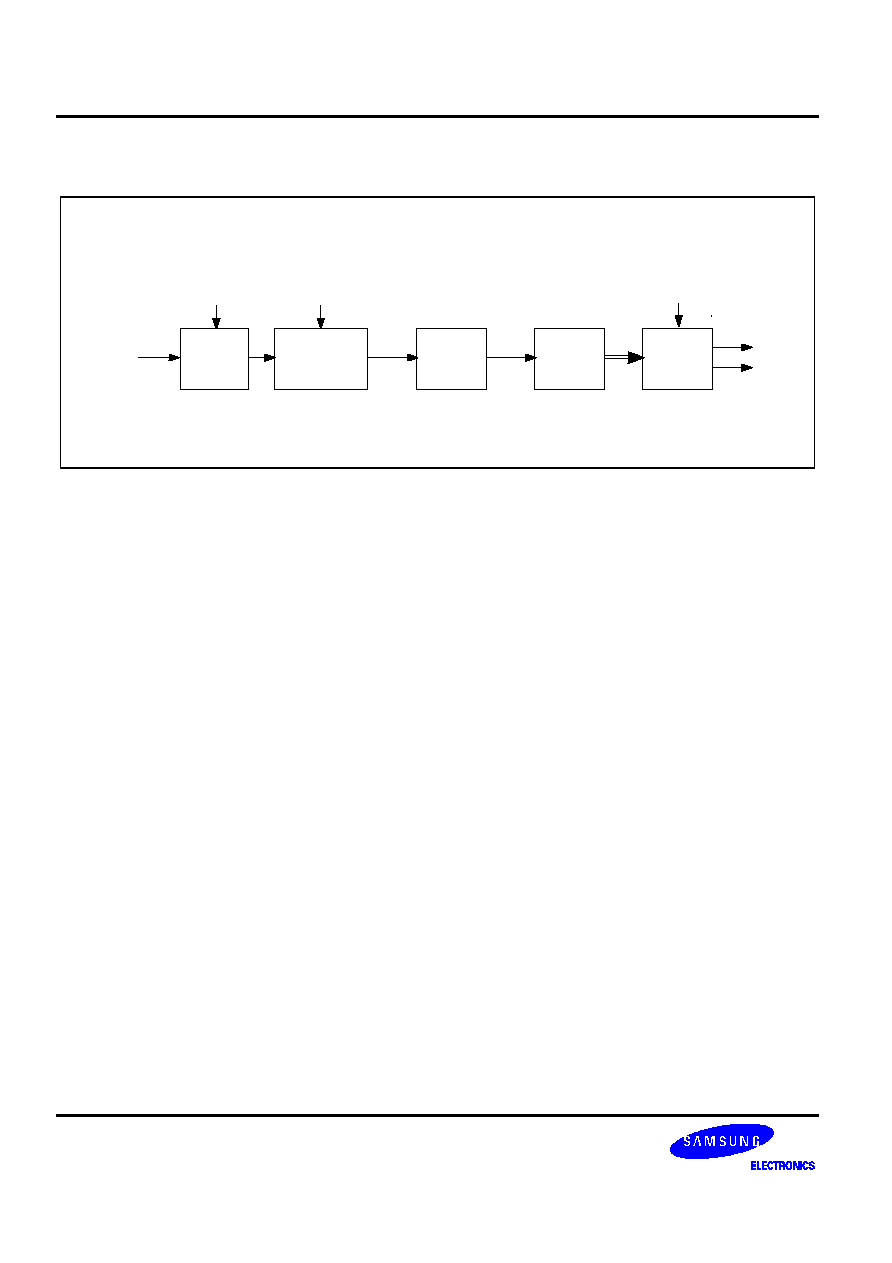
FUNCTIONAL DESCRIPTION
Compensation Filter
&
De-emphasis/
FIR Filter
Sinc Filter
&
Modulator
SC-Postfilter
Anti-Image
Filter
SDATA
BCK
LRCK
ZDENL
AoutL
4Fs/8Fs
16bits
64Fs
1bit
DEEM
DN
FSEL<1:0>
IDNUM<7:0>
1Fs/2Fs
16bits
S/P Converter
&
Attenuator
MCLK
MDATA
MLD
AoutR
MUTEL
Figure 4. Funtional Block Diagram
Fig4 is the 1bit 4th order sigma-delta DAC block daigram. S/P Converter converts serial 16bit input data to parallel
16bit data. Digital input data is attenuated by MICOM interface pin control. Compensation Filter compensates gain
droop in Passband by Sinc Filter and Sigma-Dellta Modulator Signal Transfer Function. De-emphasis Block de-
emphasizes pre-emphasised input data to emphssize high frequency in audible band. FIR Filter perfroms 4X
interpolation. And it outputs 4Fs(DN='Low') rate data or 8Fs(DN='High') rate data by variabled input data rate. It
also removes the images of the input signal that are present at multiples of the input sample frequency. And Sinc
filter makes the constant 64Fs rate data by 16 times or 8 times upsampling FIR Filter output data according to
DN(Double/Normal Mode) Pin Selection. This operation intorduces a sinc function responce on the resulting
frequency spectrum, which greatly attenuates the energy of images at the multifules of 4Fs(or 8Fs).
Digital sigma-delta modulator of bit-stream type has the IFL (Inverse-Follower-Leader) topology, and it performs a
noise-shaping function. The modulator shapes the quantization noise by suppressing its in-band component and
pushes the noise energy of outside the band-of-interest without deteriorating the audio input signal. The 64 times
oversampled 1-bit PDM outputs from the modulator drives a analog postfilter.
The analog postfilter comprises SC-postfilter, anti-imaging filter. The SC-postfilter removes the quantization noise
shaped to out-of-band by digital sigma-delta modulator. This analog filter has the good clock jitter characteristc and
very linear characteristic. And following the CTF(continuous time filter) removes the sampling images and makes
the high resolution analog output.
0.35
µ
µ
µ
µ
m 16-BIT 44.1KHZ SIGMA-DELTA STEREO DAC
BW0405XB
13
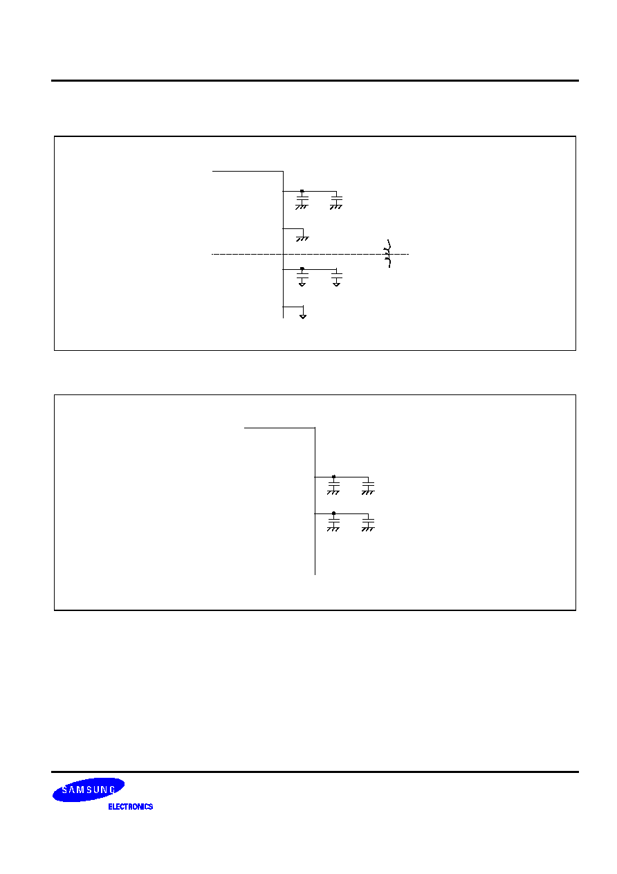
APPLICATION CIRCUIT
+
VDDA
+
0.1uF
10uF
VSSA
+
VDDD
+
0.1uF
10uF
VSSD
Analog Ground Plane
Digital Ground Plane
VSSA
VSSD
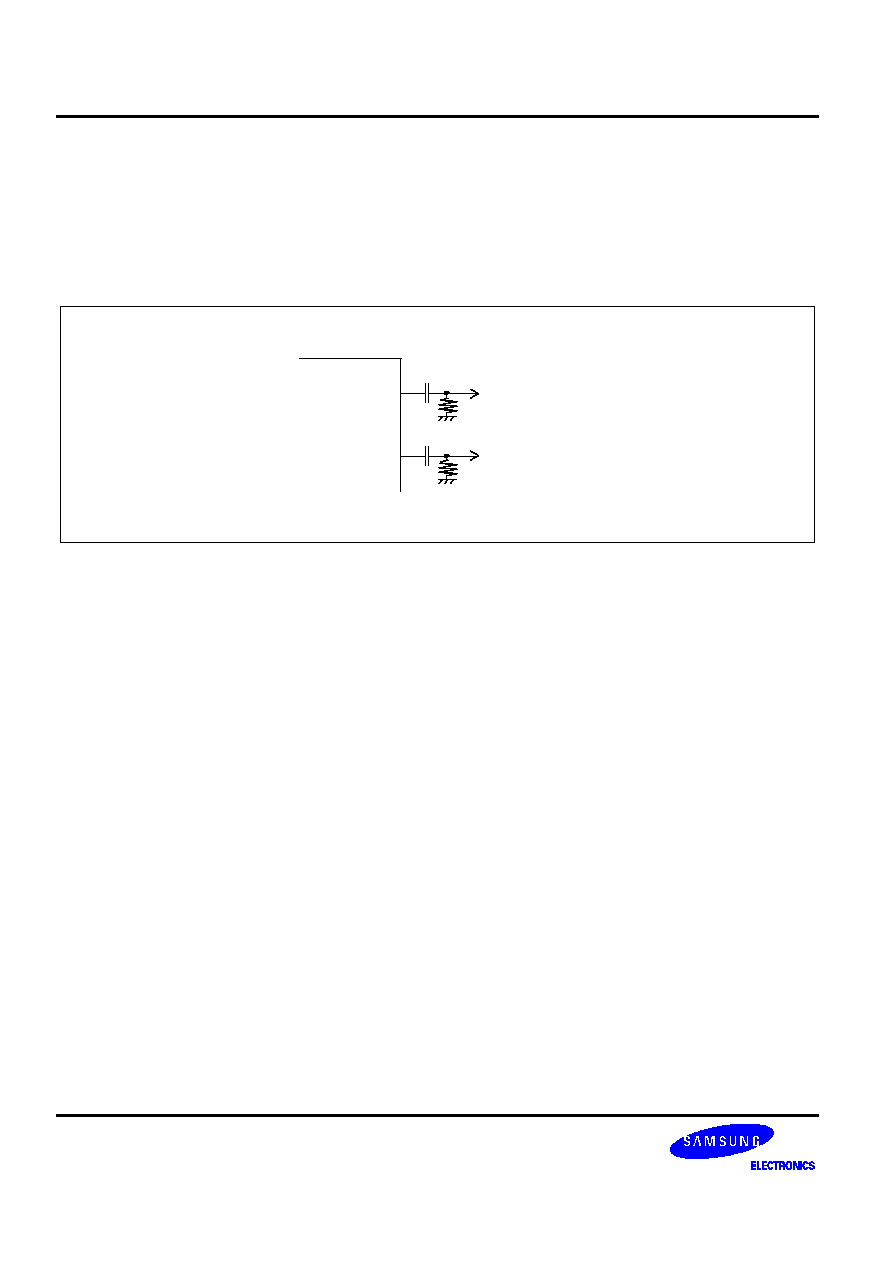
Figure 5. Bypass Capacitor for Power Supply Pins
+
VREF
+
0.1uF
+
VHALF
+
0.1uF
10uF
VSSA
VSSA
10uF
Figure 6. Bypass Capacitors for Reference Pins
BW0405XB
0.35
µ
µ
µ
µ
m 16-BIT 44.1KHZ SIGMA-DELTA STEREO DAC
14
Analog pins and digital pins must be seperated, Analog pins should be located on the analog ground plane and
digital pins should be located on the digital ground plane. Analog ground and digital ground connection is
recommended to only one path through ferrite bead like Fig5. Supply bypass capacitors should be located as close
as possible to chip. Small bypass capacitor (0.1uF) should be positioned first to chip than large bypass capacitor
(10uF).
Reference (VHALF, VREF) bypass capacitors (Fig6) should be located as close as possible to chip.
L-CH Output
1uF
100k
+
AOUTL
R-CH Output
1uF
100k
+
AOUTR
Figure 7. Ananlog output application
FIg7 is simple high pass filter circuit for analog output. It performs ac-coupling for analog output signal from analog
common level to analog ground. Recommended component values are 1uF and 100k
.
User Guide
-- This analog Core Verilog behavioral-modeling will be supplied.

0.35
µ
µ
µ
µ
m 16-BIT 44.1KHZ SIGMA-DELTA STEREO DAC
BW0405XB
15
FEEDBACK REQUEST
Sigma-Delta
DAC
Specification
We appreciate your interest in our products. If you have further questions, please specify in the attached form.
Thank you very much.
Parameter
Min
Typ
Max
Unit
Remarks
supply voltage
V
Max master clock frequency
Hz
Operating temperature
∞
C
Sampling Frequency
Hz
Dynamic range
dB
Total harmonic distortion
dB
Signal-to-noise ratio
dB
Input format resolution
(Serial/Parallel interface)
Bit
Channel
Mono Stereo
Power dissipation
mW
Full scale output voltage range
Vpp
Group delay
sec
Phase linearity deviation for
passband region
≠
(Deg)
Peak-to-peak frequency
response ripple for passband
region
dB
-- Could you explain external/internal pin configurations as required?
-- Specially requested function list:

BW0405XB
0.35
µ
µ
µ
µ
m 16-BIT 44.1KHZ SIGMA-DELTA STEREO DAC
16
NOTES