
0.35
µ
µ
µ
µ
m SIGMA-DELTA VOICE CODEC
BW0406X_LGISDN
1
GENERAL DESCRIPTION
The BW0406X_lgisdn is Sigma-Delta CODEC for speech and telephony applications. The product contains both
digital IIR/FIR filter and smoothing filter. The normal input and output channels have m/A law format with 38dB
signal to distortion ratio.
The input and output of this device is compressed form(A-law, m-law) and 14bit linear which can be easily
determined by control select pins
An on-chip voltage reference circuit is included to allow the single supply operation
FEATURES
-- Single chip voice line Codec
(A/D, D/A converter included)
-- Oversampled Sigma Delta modulator/Demodulator
-- Input/Output format : 8bit u-law/A-law and linear 14bit
- These three types are easily selectible by control pins
- When serial interface mode, the 14bit linear data has 16bit format with two don't care bits from LSB
-- Sigma Delta ADC
- 256X Oversampling
- On chip Decimation Filter
- On chip Smoothing Filter
-- Sigma Delta DAC
- 256X Oversampling
- On chip 256X Interpolation Filter
- On chip Analog Post Filter
-- Single ended Input and Output.
-- Sampling Rate of 8~11KHz
-- On chip voltage reference circuitry
-- Single +3.3V Power Supply
-- 2Vpp In, Output signal swing
-- Power Consumption
- Operating Mode : 10mW Typ(3.3V)
- Powerdown Mode : 33uW Typ(3.3V)
TYPICAL APPLICATIONS
-- Speech Processing (Recognition, Synthesis, Compression etc.)
-- Telephony
-- Modem

BW0406X_LGISDN
0.35
µ
µ
µ
µ
m SIGMA-DELTA VOICE CODEC
2
BLOCK DIAGRAM WITH INPUT/OUPUT APPLICATION
Analog
Modulator
Decimation
filter
Serial Interface
1. 14bit Linear PCM in
16bit format
2.
µ
µ
µ
µ
-law
3. A-law
VREFOUT
Voltage Reference
Output
Voltage Reference
Analog
Postfilter
Digital
Modulator
Interpolation
filter
Differential to
Single circuit +
Smoothing filter
Selectible
powerdown circuit
X256FS BCK
SYNC
RST
VDDD
VSSD
VDDA
VSSA
ADPWD DAPWD
DADS
LCS
CPSEL
SDOUT
ADC Serial
Output
SDIN
DAC Serial
Interface
ALOOP MUTE TPOST
TDECI
REFH REFL
SINPO<1:0>
SDECI<1:0>
DAPWD
AINFB1
Analog Input0
-
+
AINFB0
Analog Input1
-
+
CIS<0>
CIS<1>
APOSTOUT0
Analog Output0
APOSTOUT1
Analog Output1
COS<1:0>>
COS<1:0>
CIS<1:0>

0.35
µ
µ
µ
µ
m SIGMA-DELTA VOICE CODEC
BW0406X_LGISDN
3
CORE PIN DESCRIPTION
Name
I/O Type
I/O Pad
Pin Description
VDDA
AP
vdda
Analog Power (+3.3V)
VSSA
AG
vssa
Analog Ground (0.0V)
REFH
AP
piar50_bb
Analog Reference Power(+3.3V)
REFL
AG
piar50_bb
Analog Reference Ground (0.0V)
AMODIN0
AI
piar50_bb
ADC Analog input 0
AMODIN1
AI
piar50_bb
ADC Analog input 1
MUTE
DI
picc_bb
Analog Mute select (High active)
ALOOP
DI
picc_bb
Analog loop back select (High active)
VREFOUT
AO
poar50_bb
Vref output
AINFB0
AB
poar50_bb
Analog Input Gain control 0
AINFB1
AB
poar50_bb
Analog Input Gain control 1
APOSTOUT0
AO
poar50_bb
DAC Analog output 0
APOSTOUT1
AO
poar50_bb
DAC Analog output 1
ADPWD
DI
picc_bb
Power Down1 (High active)
DAPWD
DI
picc_bb
Power Down2 (High active)
RST
DI
picc_bb
Digital Reset (High active)
X256FS
DI
picc_bb
256*Sampling Freq.(FS) Clock
SYNC
DI
picc_bb
Sampling Freq.(FS) Clock
SDECI<1:0>
DI
picc_bb
ADC Digital Filter input select
TDECI
DI
picc_bb
ADC Digital Filter Test input
SINPO<1:0>
DI
picc_bb
DAC Post Filter input select
SDIN
DI
picc_bb
Serial Data Input
TPOST
DI
picc_bb
DAC Post Filter Test input
LCS
DI
picc_bb
Linear/Compand data select (Low/High)
CPSEL
DI
picc_bb
m-law/A-law select (Low/High)
VSSD
DG
vssd
Digital Ground
VDDD
DP
vddd
Digital Power Supply
SDOUT
DO
pot2_bb
Serial Data Output
BCK
DI
picc_bb
Bit Clock
DADS
DO
pot2_bb
DAC Modulator output
CIS<1:0>
DI
picc_bb
Analog Input Select Pins
COS<1:0>
DI
pot2_bb
Analog Output Select Pins

BW0406X_LGISDN
0.35
µ
µ
µ
µ
m SIGMA-DELTA VOICE CODEC
4
NOTES:
1. This pin description is not fixed, but recommended.
2. The Power pin(VDDA,VDDD) must be connected by DIODE_SLOT2.
3. The Ground pin (VSSA, VSSD) must be connected bye DIODE_SLOT2.
4. SDECI<1:0>, TDECI -> Decimation Filter Block test pin.
5. SINPO<1:0>, TPOST -> Post Filter Block test pin.
6. To operate the power down mode, the two control select pins, ADPWD and DAPWD must be activated simultaneously.
7. The followings are the input/output selection and mute control pins, so use these pins instead MUTE pin.
CIS<1:0>
STATUS
COS<1:0>
STATUS
0 : 0
AMODIN1 is MUTE,
AMODIN0 is MUTE
0 : 0
APOSTOUT1 is MUTE,
APOSTOUT0 is MUTE
0 : 1
AMODIN1 is MUTE,
AMODIN0 is ACTIVE
0 : 1
APOSTOUT1 is MUTE,
APOSTOUT0 is ACTIVE
1 : 0
AMODIN1 is ACTIVE,
AMODIN0 is MUTE
1 : 0
APOSTOUT1 is ACTIVE,
APOSTOUT0 is MUTE
1 : 1
AMODIN1 is ACTIVE,
AMODIN0 is ACTIVE
1 : 1
APOSTOUT1 is ACTIVE,
APOSTOUT0 is ACTIVE
I/O Type Abbr.
-- AI: Analog Input
-- DI: Digital Input
-- AO: Analog Output
-- DO: Digital Output
-- AB: Analog Bidirectional
-- DB: Digital Bidirectional
-- AP: Analog Power
-- DP: Digital Power
-- AG: Analog Ground
-- DG: Digital Ground

0.35
µ
µ
µ
µ
m SIGMA-DELTA VOICE CODEC
BW0406X_LGISDN
5
CORE CONFIGURTION
bw0406x_lgisdn
BCK
DADS
SDOUT
VREFOUT
APOSTOUT0
RST
SYNC
TPOST
TDECI
DAPWD
ADPWD
LCS
CPSEL
AINFB0
AMODIN1
REFH
REFL
X256FS
ALOOP
MUTE
SINPO<1:0>
SDECI<1:0>
SDIN
VDDD
VSSD
VDDA
VSSA
AINFB1
AMODIN0
APOSTOUT1
CIS<1:0>
COS<1:0>

BW0406X_LGISDN
0.35
µ
µ
µ
µ
m SIGMA-DELTA VOICE CODEC
6
ABSOLUTE MAXIMUM RATINGS
Characteristic
Symbol
Value
Unit
Supply Voltage
VDDD
-0.3 to 3.8
V
Digital Input Voltage
D
IN
-0.3 to 3.8
V
Storage Temperature Range
Tstg
-40 to 125
∞
C
Operating Temperature Range
Topr
0 to 70
∞
C
NOTES:
1.
ABSOLUTE
MAXIMUM
RATING
specifies
the
values
beyond
which
the
device
may
be
damaged
permanently.
Exposure
to
ABSOLUTE
MAXIMUM
RATING
conditions
for
extended
periods
may
affect
reliability.
Each
condition
value
is
applied
with
the
other
values
ke+pt
within
the
following
operating
conditions
and
function
operations
under
any
of
these
conditions
is
not
implied.
2.
All
voltages
are
measured
with
respect
to
VSS(VSSA
or
VSSD)
unless
otherwise
specified.
RECOMMENDED OPERATING CONDITIONS
Characteristics
Symbol
Min
Typ
Max
Unit
Supply Voltage
VDDA
∑
VSSA
VDDD
∑
VSSD
3.15
3.3
3.45
V
Supply Voltage Difference
VDDA
∑
VDDD
0.1
0.0
0.1
V
Digital Input Voltage Range
2.7
3.3
3.6
V
Analog Input Voltage Range
≠
2
≠
Vpp
NOTE: It
is
strongly
recommended
that
all
the
supply
pins
(VDDA,
VDDD)
be
powered
from
the
same
source
to
avoid
power
latch
up.
CONTROL CLOCK CHARACTERISTICS
Characteristics
Symbol
Min
Typ
Max
Unit
Conditions
X256FS
1.843
2.048
2.816
MHz
Fs=8KHz
Minimum Pulse Width Low
Minimum Pulse Width High
390
390
≠
160
160
ns
ns
SYNC Frequency (Fs clock)
≠
8
≠
KHz
Duty Cycle
40
≠
60
%

0.35
µ
µ
µ
µ
m SIGMA-DELTA VOICE CODEC
BW0406X_LGISDN
7
AC ELECTRICAL CHARACTERISTICS
(Measurement
Bandwidth
is
20Hz-4KHz.
Full
scale
input
sine
wave
1KHz,
FS=8KHz,
@VDDA=3.3V,
Ta=25
∞
C
,
Unless
otherwise
specified.)
Characteristics
Symbol
Min
Typ
Max
Unit
Conditions
Resolution
≠
14
≠
Bits
Sampling rate
≠
8
≠
KHz
≠
ADC Analog Input Characteristics
* Signal to Distortion
35
38
≠
dB
0dB Input : m/A Law compand
Ratio
67
70
≠
dB
0dB Input : Linear
28
29.5
≠
dB
-40dB Input : u-Law compand
29
-40dB Input : A-Law compand
23
25
≠
dB
-45dB Input : u-Law compand
24
-45dB Input : A-Law compand
Offset Error
≠
≠
±20
mV
≠
Input Voltage Range
≠
2
≠
Vpp
≠
DAC Analog Input Characteristics
* Signal to Distortion
35
38
≠
dB
0dB Input : m/A Law compand
Ratio
67
70
≠
dB
0dB Input : Linear
30
33.5
≠
dB
-40dB Input : u-Law compand
29
32
-40dB Input : A-Law compand
25
30
≠
dB
-45dB Input : u-Law compand
24
27
-45dB Input : A-Law compand
Offset Error
≠
≠
±20
mV
≠
Output Voltage Range
≠
2
≠
Vp--p
≠
Digital Filter Specification
Passband
0
0.4
Fs
Passband Ripple
+/-0.25
dB
Stopband
0.4
0.6375
Fs
Stopband Attenuation
-40
dB
Power Supply
Power comsumption
(3.3v Operating Mode)
Analog Digital
≠
≠
2.5
0.5
≠
3
0.7
mA
≠
Power comsumption
(3.3v Powerdown
Mode)
≠
10
≠
mA

BW0406X_LGISDN
0.35
µ
µ
µ
µ
m SIGMA-DELTA VOICE CODEC
8
CORE LAYOUT GUIDE
ANALOG
BLOCK
VDDA
VSSA
VBB
Guardring
DIGITAL
BLOCK
VBB
VSSD
VDDD
P+ Guardring
N-WELL Guardring
Analog Input
A
n
al
og O
u
t
put
NOTES:
1. The layout of bw0406x consists of digital part and analog part.
The digital part and the analog part must be divided.
2. The substrate of digital and analog part is seperated from digital and analog ground so that it can minimize noise
through substrate.
3. It is recommended that you use thick analog power metal. when connecting to PAD, and the path should be kept as
short as possible.
4. Digital power and analog power are used separately.
5. When the core block is connected to other blocks, it must be double guardring using N-well and P+active to remove
the substrate and coupling noise.
In that case, the power metal should be connected to PAD directly.
6. Digital input signal lines must be same length to reduce the difference of delay.

0.35
µ
µ
µ
µ
m SIGMA-DELTA VOICE CODEC
BW0406X_LGISDN
9
CORE EVALUATION GUIDE
VDDA
VSSA
AMODIN
AINFB
VREFOUT
APOSTOUT
VSSD
VDDD
MUTE
ALOOP
ADPWD
RST
X256FS
SYNC
SDECI<1:0>
TDECI
DAPWD
SINPO<1:0>
TPOST
LCS
CPSEL
DADS
BW0406X
DSP
Controller
R3
C2
C5
C6
+
REFH
REFL
C4
C3
Analog Output
C3
C4
2
2
SDIN
SDOUT
BCK
+
C4
C3
+
+
Analog Input
R1
R2
C1
+
-
VDDA
VSSA
AMODIN
AINFB
VREFOUT
APOSTOUT
VSSD
VDDD
MUTE
ALOOP
ADPWD
RST
X256FS
SYNC
SDECI<1:0>
TDECI
DAPWD
SINPO<1:0>
TPOST
LCS
CPSEL
DADS
BW0406X
DSP
Controller
R3
C2
C5
C6
+
REFH
REFL
C4
C3
Analog Output
C3
C4
2
2
SDIN
SDOUT
BCK
+
C4
C3
+
+
Analog Input
R1
R2
C1
+
-
Table 1. The Connection User Guide Line for Embedded Core Test
Location
Description
C3
0.1mF TANTALUM CAPACITOR
C4, C6
10mF CERAMIC CAPACITOR
C1
0.33mF TANTALUM CAPACITOR
C2
75pF CERAMIC CAPACITOR
R1, R2
50kW RESISTOR
R3
200kW RESISTOR
C5
0.1uF TANTALUM CAPACITOR
NOTES:
1.
If
SDOUT
is
externally
shorted
with
SDIN,
The
CODEC
is
achieved
to
loop-back
test
mode(ADC->DAC).
2.
If
end
users
want
to
test
CODEC
in
integrated
chip,
The
above
pin
must
be
extracted
to
the
PAD(pin
14).
3.
The
analog
power/ground
must
be
separated
from
digital
power/ground.
4.
CPSEL
=
1; A-law
select,
0; m-law
select
5.
I/O
TYPE
PP
and
PG
denote
PAD
Power
and
PAD
Ground
respectively.
6.
Power
typical
value:
VDDA
=
VDDD
=
3.3V,
VSSA
=
VSSD
=
0.0V

BW0406X_LGISDN
0.35
µ
µ
µ
µ
m SIGMA-DELTA VOICE CODEC
10
PACKAGE CONFIGURATION
24
23
22
21
20
19
18
17
16
15
14
13
37
38
39
40
41
42
43
44
45
46
47
48
36 35 34 33 32 31 30 29 28 27 26 25
1
2
3
4
5
6
7
8
9 10 11 12
BW0406X
SDIN
RST
DAPWD
ADPWD
NC41
NC42
X256FS
LCS
CPSEL
SYNC
BCK
SDOUT
NC24
APOSTOUT0
APOSTOUT1
NC21
VDDA
NC19
VREFOUT
VSSA
COS<1:0>
AMODIN0
AINFB0
NC13
SD
E
C
I<
1
>
SD
E
C
I<
0
>
VD
D
D
VS
SD
NC5
NC6
TD
E
C
I
NC8
A
L
OOP
CI
S<1:
0
>
AI
N
F
B1
AM
O
D
IN
1
SI
N
P
O
<
1
>
SI
N
P
O
<
0
>
VD
D
P
VS
SP
NC32
NC31
TP
O
S
T
DA
DS
NC27
MU
T
E
RE
F
H
RE
F
L
Ct
+
Cc
Cc
Ct
+
Cc
Ct
+
L
3.
3
V
Cc
Ct
+
L
24
23
22
21
20
19
18
17
16
15
14
13
37
38
39
40
41
42
43
44
45
46
47
48
36 35 34 33 32 31 30 29 28 27 26 25
1
2
3
4
5
6
7
8
9 10 11 12
BW0406X
SDIN
RST
DAPWD
ADPWD
NC41
NC42
X256FS
LCS
CPSEL
SYNC
BCK
SDOUT
NC24
APOSTOUT0
APOSTOUT1
NC21
VDDA
NC19
VREFOUT
VSSA
COS<1:0>
AMODIN0
AINFB0
NC13
SD
E
C
I<
1
>
SD
E
C
I<
0
>
VD
D
D
VS
SD
NC5
NC6
TD
E
C
I
NC8
A
L
OOP
CI
S<1:
0
>
AI
N
F
B1
SD
E
C
I<
1
>
SD
E
C
I<
0
>
VD
D
D
VS
SD
NC5
NC6
TD
E
C
I
NC8
A
L
OOP
CI
S<1:
0
>
AI
N
F
B1
AM
O
D
IN
1
SI
N
P
O
<
1
>
SI
N
P
O
<
0
>
VD
D
P
VS
SP
NC32
NC31
TP
O
S
T
DA
DS
NC27
MU
T
E
RE
F
H
RE
F
L
Ct
+
Cc
Cc
Ct
+
Cc
Ct
+
Cc
Ct
+
Cc
Ct
+
L
3.
3
V
Cc
Ct
+
L
L
LOCATION
DESCRIPTION
Ct
10uF TANTALUM CAPACITOR
Cc
0.1uF CERAMIC CAPACITOR
L
FERRITE BEAD (0.1mH)

0.35
µ
µ
µ
µ
m SIGMA-DELTA VOICE CODEC
BW0406X_LGISDN
11
CONTROL CLOCKS CHARACTERISTICS
Characteristics
Symbol
Min
Typ
Max
Unit
X256FS Frequency
Fmck
≠
2.048
≠
MHz
BCK Frequency
Fbck
≠
256
≠
KHz
SYNC Frequency
Fsync
≠
8
≠
KHz
X256FS Duty cycle (H:L)
MCDuty
40:60
50:50
60:40
%
BCK Duty cycle (H:L)
BCDuty
40:60
50:50
60:40
%
SYNC Duty cycle (H:L)
SYDuty
40:60
50:50
60:40
%
X256FS Falling and BCK Edge Delay(Hold)
Tdbck
5
10
15
ns
X256FS Falling and SYNC Edge
Delay(Hold)
Tdsync
5
10
15
ns
BCK Falling and SDOUT Delay
Tdsdout
5
10
15
ns
BCK Rising and SDIN Setup
Tsetup
10
15
20
ns
BCK Rising and SDIN Hold
Thold
10
15
20
ns

BW0406X_LGISDN
0.35
µ
µ
µ
µ
m SIGMA-DELTA VOICE CODEC
12
*Notes : BCK rising edge must NOT occur at the same time as SYNC edge.
X256FS
0.5
VDDD
Tdbck
BCK
0.5
VDDD
X256FS
0.5
VDDD
Tdsync
BCK
0.5
VDDD
BCK
0.5
VDDD
Tdsdout
SDOUT
0.5
VDDD
BCK
0.5
VDDD
Tsetup
SDIN
0.5
VDDD
Thold
X256FS
0.5
VDDD
1/Fmck
BCK
0.5
VDDD
1/Fbck
SYNC
0.5
VDDD
1/Fsync
X256FS
0.5
VDDD
MCDuty
"H"
"L"
BCK
0.5
VDDD
BCDuty
"H"
"L"
SYNC
0.5
VDDD
SYDuty
"H"
"L"

0.35
µ
µ
µ
µ
m SIGMA-DELTA VOICE CODEC
BW0406X_LGISDN
13
TIMING DIAGRAM
The frame of sync clock(SYNC) transitions determine the start of the serial data.
Input data
∑
All input data are clocked in by the falling edge of BCK.
∑
14bit, 2's complement or 8bit A-law, u-law data format.
Output data
∑
All output data are clocked out by the falling edge of BCK.
∑
14bit, 2's complement or 8bit A-law, u-law data format.
NOTES:
1.
SYNC
clock
is
at
sampling
frequency,
Fs
2.
14bit
linear
data
has
16bit
serial
data
format,
this
is
accomplished
by
16FS
(
=
Fs
clock
x
16
)
and
two
don't care bits
are
added
from
LSB,
to
fit
into
16bit
format.

BW0406X_LGISDN
0.35
µ
µ
µ
µ
m SIGMA-DELTA VOICE CODEC
14
Codec serial interface timing diagram
7
6
5
4
3
2
1
0
X
X
X
X
X
X
X
X
7
6
5
4
3
2
1
0
X
X
X
X
X
X
X
X
13
12
11
10
9
8
7
6
5
4
3
2
1
0
X
X
13 ; MSB, 0 ; LSB
13
12
11
10
9
8
7
6
5
4
3
2
1
0
X
X
Fs Clock
SYNC
16Fs
BCK
7 ; MSB, 0 ; LSB
X : Don't care data
X : Don't care data
SDOUT[ADC output](Compressed data)
X : Non-valid data
(0 insetion)
SDOUT[ADC output](Linear data)
SDIN [DAC input](Linear data)
SDIN [DAC input](Compressed data)
13 ; MSB, 0 ; LSB
7 ; MSB, 0 ; LSB
X : Non-valid data
(0 insetion)
Codec clock interface timing diagram
16Fs
BCK
256Fs
X256FS
Fs
SYNC

0.35
µ
µ
µ
µ
m SIGMA-DELTA VOICE CODEC
BW0406X_LGISDN
15
INPUT/OUTPUT APPLICATION GUIDE
1. Input stage application guide
-
+
R1
AMODIN0 and AMODIN1
Analog Input
R1
AINFB0 and AINFB1
- +
C1
Typhical value of R1 and C1
R1 > 50K
C1 = 0.33mF
2. Output stage application guide
Speaker
Driver
Amp
APOSTOUT0
and APOSTOUT1
R3
C2
Ground
How to determine the value of R3 and C2.
C2 = 1.5*10-5/R3
For example : If you choose R3 as 200K
, then the value of C3 is 75pF.
3. VREFOUT port application guide
VREFOUT
C1
Ground
C2
C1 = 0.1mF, C2 = 10mF
Note : The user should dispose the C1 and C2 as the order shown above and dispose the capacitors to VREFOUT
pin as close as possibe.

BW0406X_LGISDN
0.35
µ
µ
µ
µ
m SIGMA-DELTA VOICE CODEC
16
PHANTOM CELL INFORMATION

0.35
µ
µ
µ
µ
m SIGMA-DELTA VOICE CODEC
BW0406X_LGISDN
17
LAYOUT GUIDE
∑
∑
BW0406X_LGISDN
0.35
µ
µ
µ
µ
m SIGMA-DELTA VOICE CODEC
18
FEEDBACK REQUEST
It should be quite helpful to our CODEC core development if you specify your system requirements on CODEC in
the following characteristic checking table and fill out the additional questions.
We appreciate your interest in our products. Thank you very much.
-- Could
you
explain
external/internal
pin
configurations
as
required?
Specially
requested
function
list
:
1. What
is
your
signal
band
to
use,
3.6KHz?
4KHz?
or
4.8KHz?
2.
What
is
your
analog
in/output
signal
voltage
swing?
and
what
kind
of
format
do
your
want
as
analog
signal
in/ouput:
single
or
differential
format? If you can, Please let us know, what is your exact in/output signal spec.
3. What is your minimum S/N+D spec?
4. Do you want linear phase characteristic or you don't care on digital filter spec?
5. Could you give us exact design spec of speech codec? (For example, A-law, u-law and so on.)
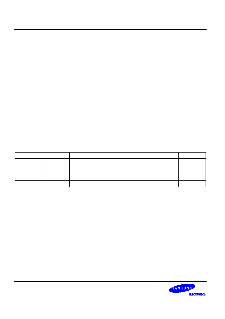
REVISION HISTORY
Version
Date
Modified Items
Comments
Ver 1.0
02.04.28
- p5: Digital Filter Specification added
- p12: Phantom Cell Information added
- p13: Layout Guide added
Ver 1.1
02.07.30
- p1: a typo corrected