 | ÐлекÑÑоннÑй компоненÑ: BW1217X | СкаÑаÑÑ:  PDF PDF  ZIP ZIP |
/home/web/htmldatasheet/RUSSIAN/html/samsung/188097

0.35
µ
µ
µ
µ
m 10-BIT 30MSPS ADC
BW1217X
1
GENERAL DESCRIPTION
The bw1217x is a CMOS 10-bit A/D converter for video applications. It is a three-step pipelined A/D converter
which consists of sample & hold, two multiplying DACs, and three 4-bit flash ADCs.
The maximum conversion rate of bw1217x is 30MSPS and supply voltage is 3.3V single.
TYPICAL APPLICATIONS
-- PC or computer based video signal processing such as multi-media, scanner, etc.
-- General Purpose video applications including camcorder, digital video, broad-casting and studio equipments.
-- Medical electronics such as digital scope, transit recorder, radar.
FEATURES
-- Resolution: 10Bit
-- Differential Linearity Error:
±
1.0 LSB
-- Integral Linearity Error:
±
2.0 LSB
-- Maximum Conversion Rate: 30MSPS
-- Sample & Hold Function Implemented
-- Low Power Consumption: 82.5mW(Typ)
-- Power Supply: 3.3V Single
-- Operation Temperature Range: 0
°
C~70
°
C
BW1217X
0.35
µ
µ
µ
µ
m 10-BIT 30MSPS ADC
2
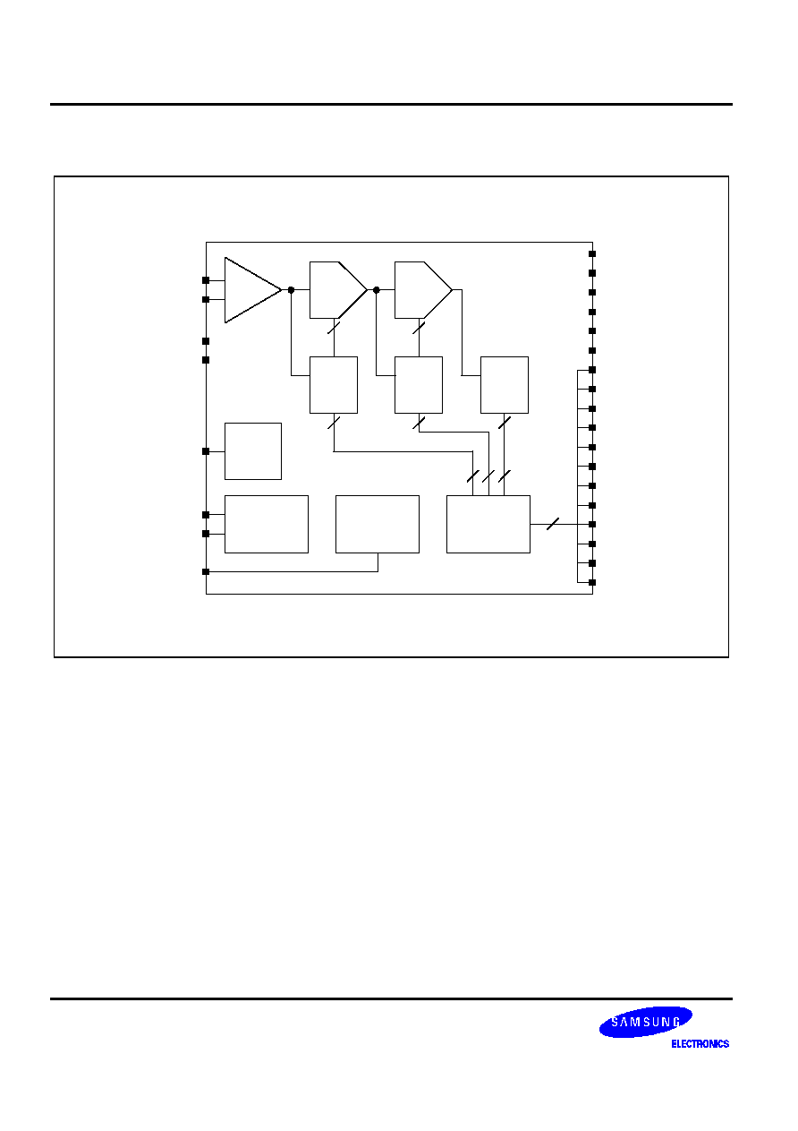
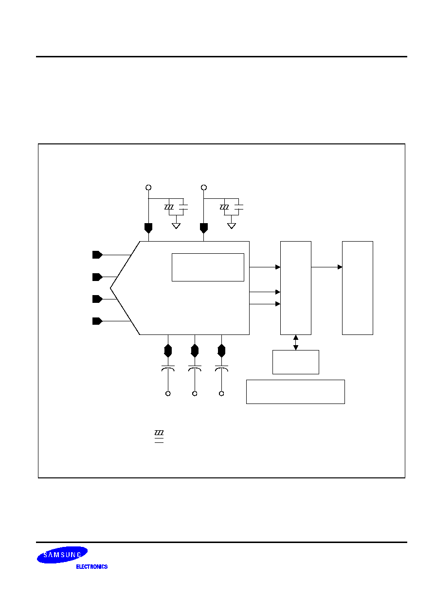
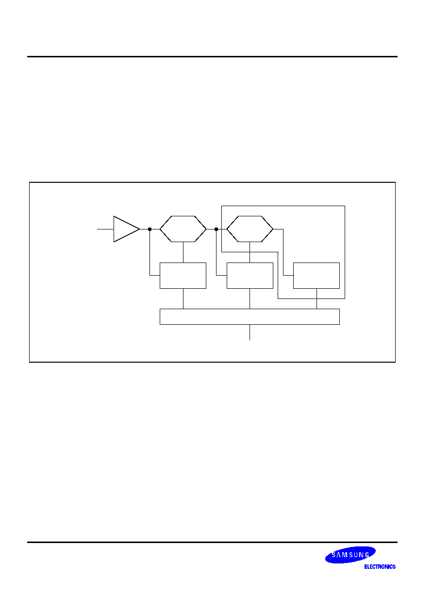
FUNCTIONAL BLOCK DIAGRAM
SHA
MDAC
1
MDAC
2
Flash
1
Flash
2
Flash
3
Clock
GEN.
Main
Bias
CML
GEN.
Digital
Logic
AINT
AINC
REFTOP
REFBOT
CKIN
VDDA
VBBA
VSSA
VDDD
VSSD
VBBD
OVF
UDF
DO[9]
DO[8]
DO[7]
DO[6]
DO[5]
DO[4]
DO[3]
DO[2]
DO[1]
DO[0]
ITEST
STBY
CML

0.35
µ
µ
µ
µ
m 10-BIT 30MSPS ADC
BW1217X
3
CORE PIN DESCRIPTION
Name
I/O Type
I/O PAD
Pin Description
AINT
AI
piar50_bb
Analog
Input
+
Input
Range:
1.9V
~
1.4V
AINC
AI
piar50_bb
Analog
Input
Input Range: 1.4V ~ 1.9V
REFMID
AB
pia_bb
Reference
Mid
Point
(Test
Pin)
REFTOP
AI
pia_bb
Reference
Top
(1.9V)
REFBOT
AI
pia_bb
Reference
Bottom(1.4V)
VDDA
AP
vdda
Analog
Power
(3.3V)
VSSA
AG
vssa
Analog
Ground
VBBA
AG
vbba
Analog
Sub
Bias
ITEST
AB
pia_bb
open = use
internal
bias
point
STBY
DI
picc_bb
high = power
saving
standby
mode
(normally
=
gnd)
CKIN
DI
picc_bb
Sampling
Clock
Input
CML
AB
pia_bb
Internal
Bias
Point (Test
Pin)
DO[9:0]
DO
pot2_bb
Digital
Output
OVF
DO
pot2_bb
Overflow
UDF
DO
pot2_bb
Underflow
VBBD
DG
vbba
Digital
Sub
Bias
VSSD
DG
vssd
Digital
Ground
VDDD
DP
vddd
Digital
Power
I/O Type Abbr.
-- AI: Analog Input
-- DI: Digital Input
-- AO: Analog Output
-- DO: Digital Output
-- AB: Analog Bidirectional
-- DB: Digital Bidirectional
-- AP: Analog Power
-- DP: Digital Power
-- AG: Analog Ground
-- DG: Digital Ground
BW1217X
0.35
µ
µ
µ
µ
m 10-BIT 30MSPS ADC
4
CODE CONFIGURATION
BW1217X
STBY
CKIN
REFBOT
REFTOP
AINC
AINT
CM
L
REF
M
ID
ITES
T
VBB
D
VSS
D
VBB
A
VSS
A
VDD
D
VDD
A
UDF
OVF
DO[9:0]
0.35
µ
µ
µ
µ
m 10-BIT 30MSPS ADC
BW1217X
5
ABSOLUTE MAXIMUM RATINGS
Characteristic
Symbol
Value
Unit
Supply Voltage
VDD
4.5
V
Analog Input Voltage
AIN
VSS to VDD
V
Digital Input Voltage
CLK
VSS to VDD
V
Digital Output Voltage
V
OH,
V
OL
VSS to VDD
V
Storage Temperature Range
Tstg
-45 to 125
°
C
NOTES:
1.
ABSOLUTE
MAXIMUM
RATING
specifies
the
values
beyond
which
the
device
may
be
damaged
permanently.
Exposure
to
ABSOLUTE
MAXIMUM
RATING
conditions
for
extended
periods
may
affect
reliability.
Each
condition
value
is
applied
with
the
other
values
kept
within
the
following
operating
conditions
and
function
operation
under
any
of
these
conditions
is
not
implied.
2.
All
voltages
are
measured
with
respect
to
VSS
unless
otherwise
specified.
3.
100pF
capacitor
is
discharged
through
a
1.5K
resistor
(Human
body
model)
RECOMMENDED OPERATING CONDITIONS
Characteristics
Symbol
Min
Typ
Max
Unit
Supply Voltage
VDDA - VSSA
VDDD - VSSD
3.15
3.3
3.45
V
Supply Voltage Difference
VDDA - VDDD
-0.1
0.0
0.1
V
Reference Input Voltage(Externally)
REFTOP
REFBOT
1.9
1.4
V
Analog Input Voltage (+)
AINT
1.4
1.9
V
Analog Input Voltage (-)
AINC
1.9
1.4
V
Operating Temperature
Topr
0
70
°
C
NOTE: It
is
strongly
recommended
that
all
the
supply
pins
(VDDA,
VDDD)
be
powered
from
the
same
source
to
avoid
power
latch-up.
BW1217X
0.35
µ
µ
µ
µ
m 10-BIT 30MSPS ADC
6
DC ELECTRICAL CHARACTERISTICS
Characteristics
Symbol
Min
Typ
Max
Unit
Conditions
Resolution
10
Bits
Reference Current
IREF
2
3
mA
Differential Linearity Error
DLE
±1.0
LSB
AINT: 0.2 ~ 1.2V
(Ramp Input)
Integral Linearity Error
ILE
±2.0
LSB
Fck: 1MHz
Bottom Offset Voltage Error
EOB
20
LSB
Top Offset Voltage Error
EOT
20
LSB
NOTES:
1.
Converter
Specifications
(unless
otherwise
specified)
VDDA=3.3V
VDDD=3.3V
VSSA=GND
VSSD=GND
Ta=25
°
C
2.
TBD:
To
Be
Determined
AC ELECTRICAL CHARACTERISTICS
Characteristics
Symbol
Min
Typ
Max
Unit
Conditions
Maximum Conversion Rate
fc
30
MSPS
AINT: 1MHz Sine Signal
(source resolution > 12-
bit)
Dynamic Supply Current
Ivdd
25
30
mA
fc = 30MHz
(without system load)
Signal - to - Noise Ratio
SNR
48
52
54
dB
AINT = 1MHz
fc = 30MHz
0.35
µ
µ
µ
µ
m 10-BIT 30MSPS ADC
BW1217X
7
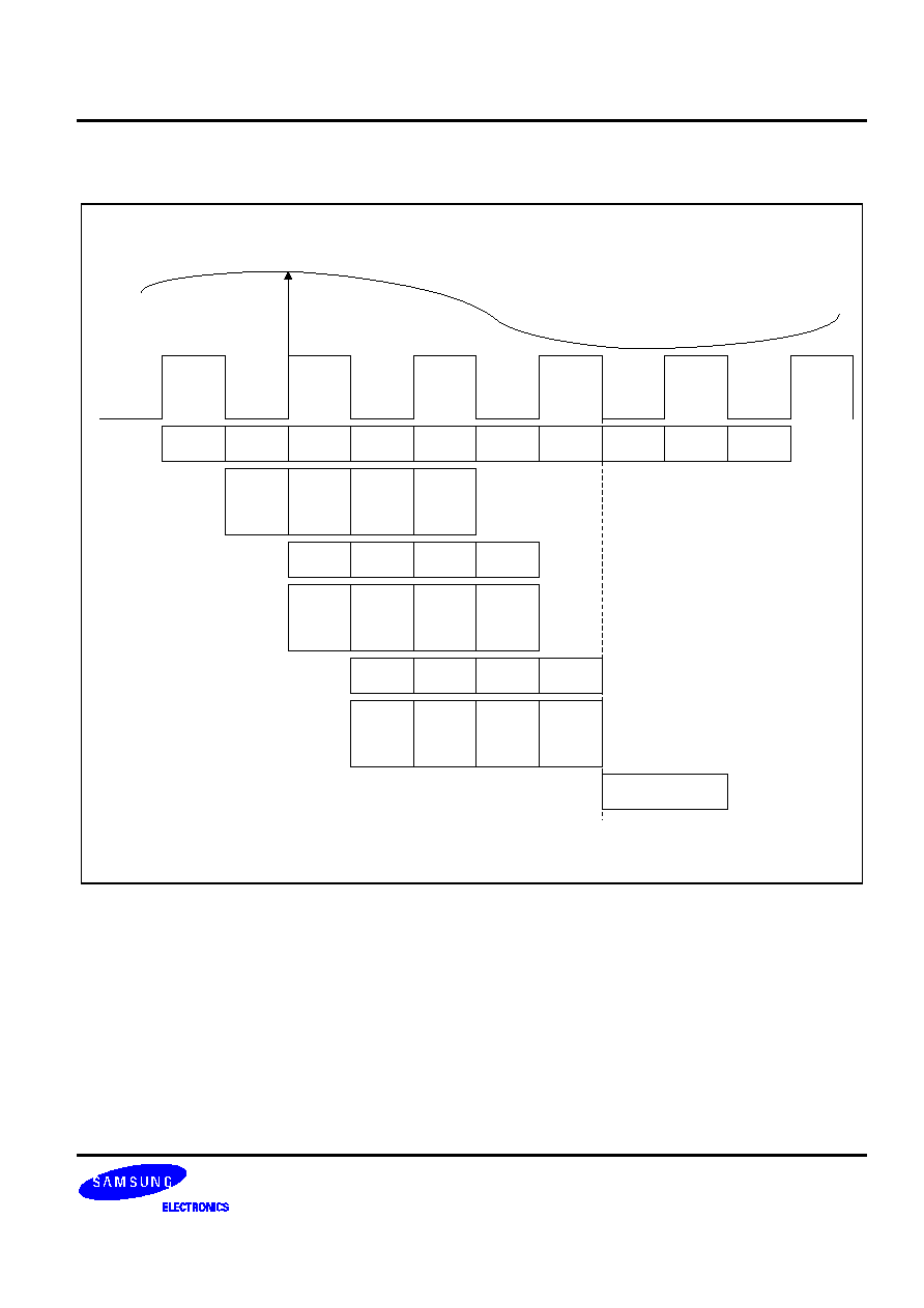
TIMING DIAGRAM (MAIN FUNCTION)
SHA
CLOCK
AINT
hold
track
ref sample amplify
precharge
latch
track
latch
encoding
hold
track
hold
track
hold
track
input
sample
residue
amplify
input
sample
residue
amplify
ref sample amplify
precharge
latch
track
latch
encoding
input
sample
residue
amplify
input
sample
residue
amplify
ref sample amplify
precharge
latch
track
latch
encoding
hold
track
DATA
FLASH1
MDAC1
FLASH2
MDAC2
FLASH3
DATA

BW1217X
0.35
µ
µ
µ
µ
m 10-BIT 30MSPS ADC
8
FUNCTIONAL DESCRIPTION
1. bw1217x is a three step A/D Converter comprising three 4-bit flash ADC and two multiplying DAC. The N-bit
flash ADC is composed of 2
(n-1)
latching comparators, and multiplying DAC is composed of 2*(N+2) capacitors
and two fully-differential amplifier.
2. bw1217x operates as follows. During the first "L" cycle of external clock the analog input data is tracked and
sampled, and the input is held from the rising edge of the external clock, which is fed to the first 4-bit flash
ADC, and the first multiplying DAC. Multiplying DAC reconstructs a voltage corresponding to the first 4-bit
ADC's output, and finally amplifies a residue voltage by 2
3
. The second 4-bit flash ADC, and MDAC are
worked
as same manner, finally amplifiers a residue voltage, which is the difference between first MDAC's output and
reconstructed voltage by 2
2
. The third 4-bit flash ADC, and MDAC are worked as previous stages.
3. bw1217x has the error correction scheme, which handles the output from mismatch in the first, second and
third flash ADC.
MAIN BLOCK DESCRIPTION
1. SAH
SAH(track and hold) is the circuit that samples the analog input signal and holds that value until next sample-
time. It is good as small as its different value between analog input signal and output signal. SAH amp gain
must be higher than 66dB at least for less than 1/2LSB of SAH error voltage at 10bit ADC and its conversion
frequency is 30MHz, its settling-time must be shorten than 12ns. This SAH is consist of fully differential op
amp, switching tr. and sampling capacitor. The sampling clock are non-overlapping clocks(Q1,Q2) and
sampling capacitor value is 1.2pF. SAH uses independentbias to protect interruption of any other circuit. SAH
amp is designed that open-loop dc gain is higher than 70dB, phase margin is higher than 60degree. Its input
block is designed to be the rail-to-rail architecture using complementary differential pair.
2. FLASH
The 4-bit flash converter compares analog signal(SAH output) with reference voltage, and that result transfers
to MDAC and digital correction logic block. It is realized fully differential comparators of 15EA. Considering self-
offset, dynamic feed through error, it should distinguish 40mV at least. First, the comparators charge the
reference voltage at the sampling capacitors before transferred SAH output. Q2 works this process and Q1
discharges this sampling capacitors. That is, the comparators compare relative different values dual input
voltage with dual reference voltage. Its output during Q1 operation is stored at the pre-latch block by Q1P.
3. MDAC
MDAC is the most important block at this ADC and it decides the characteristics. MDAC is consist of
amp1,amp2, selection logic and capacitor array(c_array). C_array's compositions are the capacitors to charge
the analog input and the reference voltage, Switches to control the path. Selection logic controls the c_array
internal switches. If Q1 is high, selection's output is all low, the switches of tsw1 are off, the switches of tsw2
are all on. Therefore the capacitors of c_array charges analog input values held at SAH. If Q2 is high, it is
reversed and final MDAC output voltage is described the following equation.
Vout = (AIN - Vref)*8-Vref/2
AIN=AINT-1.5V
0.35
µ
µ
µ
µ
m 10-BIT 30MSPS ADC
BW1217X
9
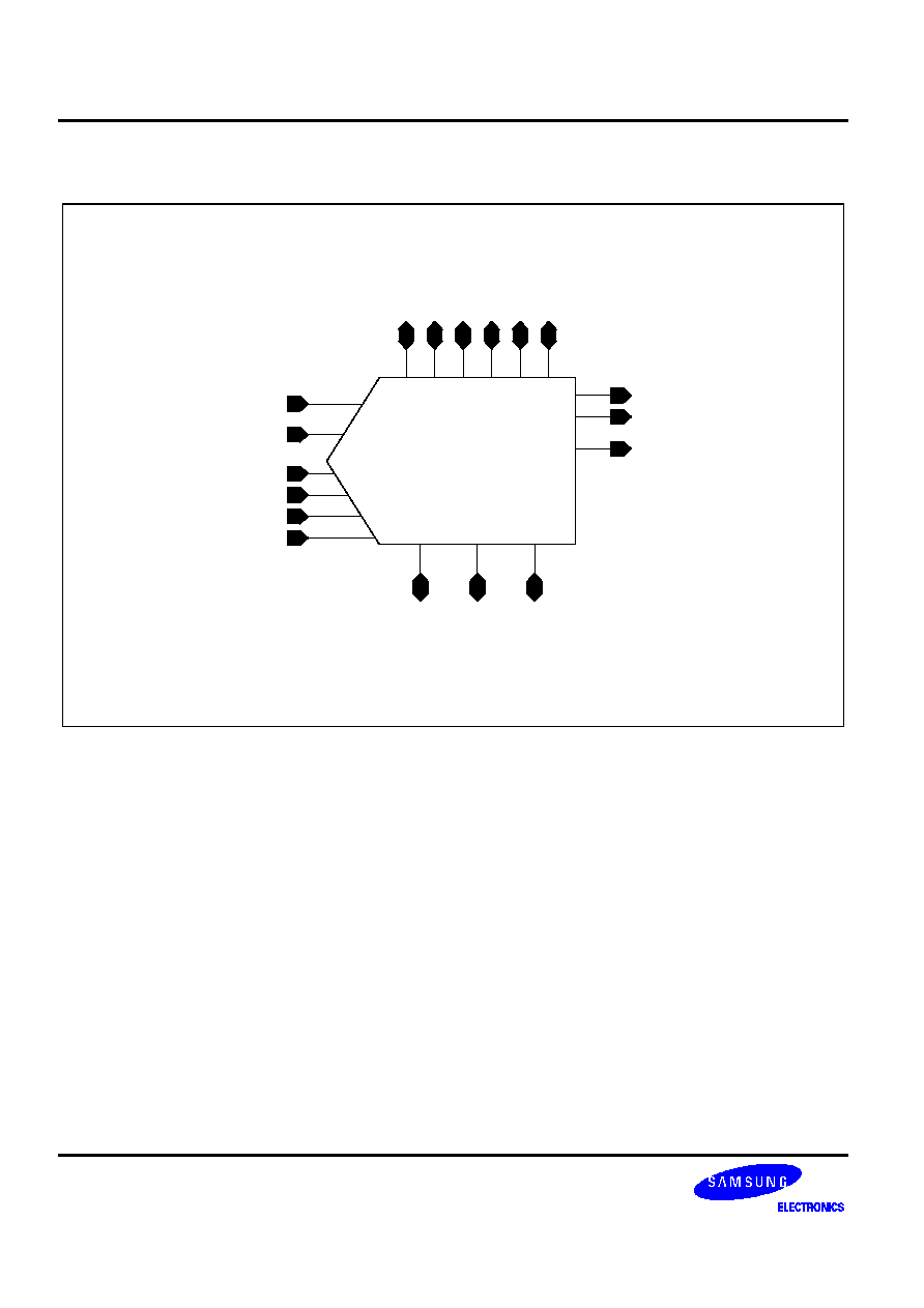
CORE EVALUATION GUIDE
1. ADC function is evaluated by external check on the bidirectional pads connected to input nodes of HOST DSP
back-end circuit.
2. The reference voltages may be biased internally through resistor divider.
BW1217X
1.9V
CM
L
REF
M
ID
ITES
T
REFTOP
OVF
UDF
REFBOT
1.4V
Power Used:
VDDA, VDDD, VBBD,
VSSA, VSSD, VBBA
DO[9:0]
Digital
Mux
HOST
DSP
CORE
DO[9:0]
Bidirectional
PAD
DO[9:0]
(ADC Function Test &
Externally Forced Digital Input)
CKIN
AINC
AINT
STBY
NOTES:
1. : 10uF electrolytic capacitor unless otherwise specified
2. : 0.1uF ceramic capacitor unless otherwise specifed
BW1217X
0.35
µ
µ
µ
µ
m 10-BIT 30MSPS ADC
10
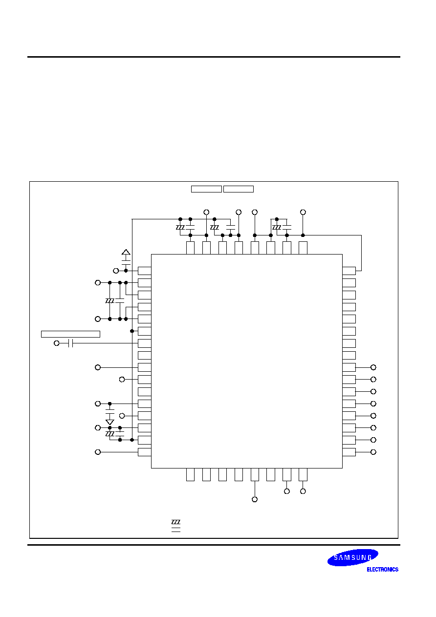
PACKAGE CONFIGURATION
NOTES
1.
You
can
test
ADC
function
by
checking
external
bidirectional
pad
connected
to
internal
signal
path.
2.
ESD
(Electro Static
Discharge)
sensitive
device.
Although
the
digital
control
inputs
are
diode
protected,
permanent
damage
may
occur
on
devices
subjected
to
high
electrostatic
discharges.
It
is
recommended
that
unused
devices
be
stored
in
conductive
foam
or
shunts
to
avoid
performance
degradation
or
loss
of
functionality.
The
protective
foam
should
be
discharged
to
the
destination
socket
before
devices
are
inserted.
3. NC
denotes
"No
Connection".
BW1217X
VBBD
NC
NC
NC
NC
OVF
UDF
D<9>
D<8>
D<5>
D<4>
D<3>
D<2>
NC
D<7>
D<6>
44
43
42
41
40
39
38
37
36
35
34
33
32
31
30
29
CML
VDDA
VDDA
VBBA
VSSA
AINT
NC
AIN
REFMID
STBY
VDDR
VSSR
CKIN
VSSA
NC
ITEST
5
6
7
8
9
10
11
12
13
14
15
16
17
18
19
20
Video-in
GND
3.3V
Analog Power
Reference
Bottom
Reference
Top
3.3V
Digital
Power
GND
NC
NC
NC
TR
I
S
TA
TE
NC
D<
0>
D<
1>
NC
27
26
28
25
24
23
22
21
RE
FB
OT
RE
FT
OP
NC
VD
DD
VD
DD
VS
SD
VS
SD
NC
46
47
45
48
1
2
3
4
Digital Output Bits 0 and 1
D
i
g
i
t
a
l
O
u
tp
ut
B
i
ts 2 T
h
r
oug
h 9
NOTES:
1. : 10uF electrolytic capacitor unless otherwise specified
2. : 0.1uF ceramic capacitor unless otherwise specifed
0.35
µ
µ
µ
µ
m 10-BIT 30MSPS ADC
BW1217X
11
PACKAGE PIN DESCRIPTION
Name
Pin No.
I/O Type
Pin Description
REFTOP
2
AI
External Reference Top Bias.(1.9V)
REFBOT
3
AI
External Reference Bottom Bias.(1.4V)
CML
5
AB
Internal Bias Point (Test Pin)
VDDA
6,7
AP
3.3V Analog Power
VBBA
8
AG
Analog Sub Bias
VSSA
9,10
AG
Analog Ground
AINT
11
AI
Analog Input (+)
Input Range: 1.4~1.9V
AINC
13
AI
Analog Input. (-)
Input Range: 1.9~1.4V
REFMID
14
AB
Reference Mid Point (Test Pin)
ITEST
16
AB
open=use internal bias point
STBY
17
DI
High = power saving standby mode (normally gnd)
VDDR
18
PP
Ouput Driver Power (3.3V)
VSSR
19
PG
Output Driver Ground
CKIN
20
DI
Sampling Clock Input
TRISTATE
25
DI
high = high impedance digital output
(normally gnd)
DO[9:0]
27~36
DO
Digital Output
UDF
37
DO
Underflow
OVF
38
DO
Overflow
VBBD
44
DG
Digital Substrate Bias
VSSD
45,46
DG
Digital Ground
VDDD
47,48
DP
Digital Power(3.3V)
NOTE: I/O
TYPE
PP
and
PG
denote
PAD
Power
and
PAD
Ground
respectively.
BW1217X
0.35
µ
µ
µ
µ
m 10-BIT 30MSPS ADC
12
USER GUIDE
1. Resolution Control.
-- Modular structure is the most important feature of bw1217x.
-- You can get any resolution you want by combining each primary module (MDAC + FLASH) without major
circuit change.
-- It means you don't have to redesign the most difficult analog block for another resolution.
-- But this simple resolution control method has a limit up to 10bits, otherwise the internal op-amp must be
redesigned.
mdac1
flash1
mdac2
flash2
flash3
dclogic
module
10-bit
sha
ain
2. Speed Up
-- The initial target speed of bw1217x was 30MHz, but it proved to operate well at 35MHz or more due to a
lot of design margin.
3. Input Range Variation.
-- The default of the input of this ADC is differential -0.5V ~ +0.5V.
-- The bias voltages of both AINT and AINC are 0.2V~1.2V, and their offset is 0.7V.
-- In order to change to another input voltage range, alter the voltage values of AINT and AINC after setting
Reftop and Refbot to the maximum value of input range.
-- If you want single ended input, fix AINC to 0.7V as a ground and the internal input voltage level is V(aint)-0.7V.
4. Verilog Modeling
-- Verilog modeling needs 64bits for only one analog real signal.
0.35
µ
µ
µ
µ
m 10-BIT 30MSPS ADC
BW1217X
13
FEEDBACK REQUEST
It should be quite helpful to our ADC core development if you specify your system requirements on ADC in the
following characteristic cheking table and fill out the additional questions.
We appreciate your interest in our products. Thank you very much.
Characteristic
Min
Typ
Max
Unit
Remarks
Analog Power Supply Voltage
V
Digital Power Supply Voltage
V
Bit Resolution
Bit
Reference Input Voltage
V
Analog Input Voltage
Vpp
Operating Temperature
°
C
Integral Non-linearity Error
LSB
Differential Non-linearity Error
LSB
Bottom Offset Voltage Error
mV
Top Offset Voltage Error
mV
Maximum Conversion Rate
MSPS
Dynamic Supply Current
mA
Power Dissipation
mW
Signal-to-noise Ratio
dB
Pipeline Delay
CLK
Digital Output Format (Provide detailed
description & timing diagram)
1. Between single input-output and differential input-output configurations, which one is suitable for your system
and why?
2. Please comment on the internal/external pin configurations you want our ADC to have, if you have any reason
to prefer some type of configuration.
3. Freely list those functions you want to be implemented in our ADC, if you have any.

BW1217X
0.35
µ
µ
µ
µ
m 10-BIT 30MSPS ADC
14
NOTES