 | ÐлекÑÑоннÑй компоненÑ: BW1218L | СкаÑаÑÑ:  PDF PDF  ZIP ZIP |
/home/web/htmldatasheet/RUSSIAN/html/samsung/188098

0.35
µ
µ
µ
µ
m 10-BIT 510MSPS ADC
BW1218L
1
GENERAL DESCRIPTION
The BW1218L is a CMOS 10-bit analog-to-digital converter (ADC). It converts the analog input signal into 10bit
binary digital codes at a maximum sampling rate of 10MHz.
The device is a monolithic ADC with an on-chip, high-performance, sample-and-hold Amplifier (SHA) and current
reference. The structure allows single-ended input for simple interface.
TYPICAL APPLICATIONS
-- HDD Engine
-- Multi-Media (CDP)
-- Low Power Application
FEATURES
-- Resolution: 10-bit
-- Maximum Conversion Rate: 10MHz
-- Package Type: 48TSSOP
-- Power Supply: 3.3V
-- Power Consumption: 40mW (typical)
-- Reference Voltage: 3.2V (single reference)
-- Input Range: 0V ~ 3.0V (3.0VP-P)
-- Differential Linearity Error:
±
0.7 LSB
-- Integral Linearity Error:
±
1.1 LSB
-- Signal to Noise & Distortion Ratio : 54dB
-- Digital Output: CMOS Level
-- Operating Temperature Range : 0
°
C ~ 70
°
C
BW1218L
0.35
µ
µ
µ
µ
m 10-BIT 510MSPS ADC
2
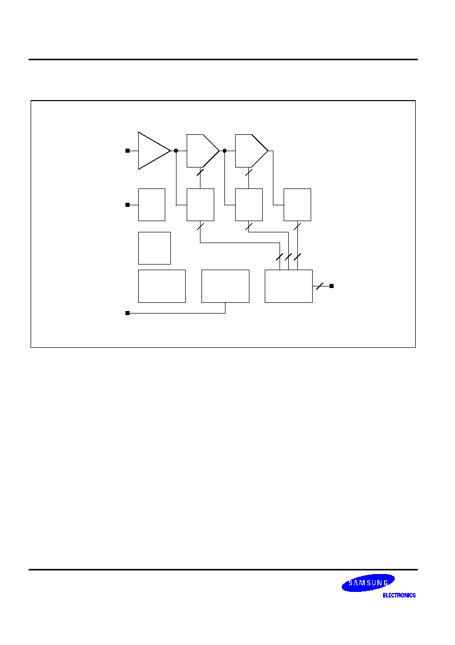
FUNCTIONAL BLOCK DIAGRAM
SHA
MDAC
1
MDAC
2
Flash
1
Flash
2
Flash
3
Clock
GEN.
Main
Bias
CML
GEN.
Digital
Logic
Analog
Input
Reference
Input
Clock
Digital
Output
REF
GEN
0.35
µ
µ
µ
µ
m 10-BIT 510MSPS ADC
BW1218L
3
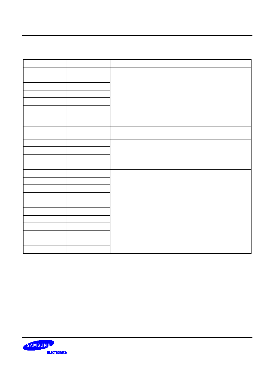
CORE PIN DESCRIPTION
Name
I/O Type
I/O Pad
Pin Description
VREF
AI
pia_bb
Reference Voltage (3.2V)
AGND
AI
pia_bb
Analog Ground for Reference
VDDA
AP
vdda
Analog Power (3.3V)
VBBA
AG
vbba
Analog Sub Bias
VSSA
AG
vssa
Analog Ground
AINT
AI
piar50_bb
Analog Input
(Input Range: 0.0V ~ 3.0V)
SPEEDUP
DI
picc_bb
VDD=Speed up, GND=Normal
STBY
DI
picc_bb
VDD=power saving (standby),
GND=normal
CKIN
DI
picc_bb
Sampling Clock Input
DO[9:0]
DO
pot4_bb
Digital Output
EOC
DO
pot4_bb
End of Conversion Signal
STCB
DI
picc_bb
Start of Conversion Signal
VBBD
DG
vbba
Digital Sub Bias
VSSD
DG
vssd
Digital GND
VDDD
DP
vddd
Digital Power (3.3V)
I/O Type Abbr.
-- AI: Analog Input
-- DI: Digital Input
-- AO: Analog Output
-- DO: Analog Output
-- AP: Analog Power
-- AG: Analog Ground
-- DP: Digital Power
-- DG: Digital Ground
-- AB: Analog Bidirection
-- DB: Digital Bidirection
BW1218L
0.35
µ
µ
µ
µ
m 10-BIT 510MSPS ADC
4
CODE CONFIGURATION
BW1218L
AINC
CKI
N
SPE
EDUP
STB
Y
DO[9:0]
[MSB:LSB]
EOC
AGND
VREF
STC
B
VDD
A
VSS
A
VBB
A
VDD
D
VSS
D
VBB
D
0.35
µ
µ
µ
µ
m 10-BIT 510MSPS ADC
BW1218L
5
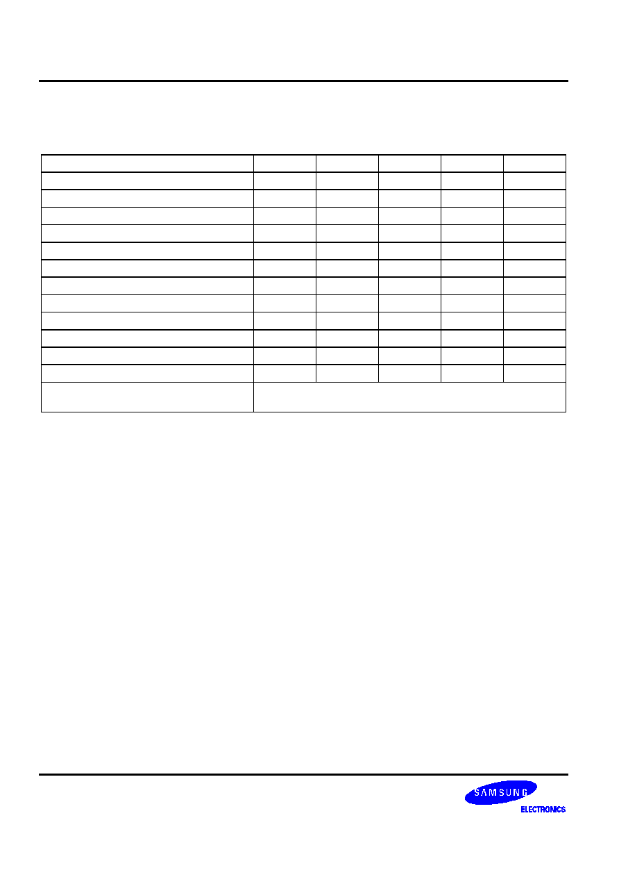
ABSOLUTE MAXIMUM RATINGS
Characteristics
Symbol
Value
Unit
Supply Voltage
VDD
4.5
V
Analog Input Voltage
AIN
VSS to VDD
V
Digital Input Voltage
CKIN
VSS to VDD
V
Reference Voltage
VREF/AGND
VSS to VDD
V
Storage Temperature Range
Tstg
-45 to 150
°
C
Operating Temperature Range
Topr
0 to 70
°
C
NOTES
1.
ABSOLUTE
MAXIMUM
RATING
specifies
the
values
beyond
which
the
device
may
be
damaged
permanently.
Exposure
to
ABSOLUTE
MAXIMUM
RATING
conditions
for
extended
periods
may
affect
reliability.
Each
condition
value
is
applied
with
the
other
values
kept
within
the
following
operating
conditions
and
function
operation
under
any
of
these
conditions
is
not
implied.
2.
All
voltages
are
measured
with
respect
to
VSS
unless
otherwise
specified.
3.
100pF
capacitor
is
discharged
through
a
1.5k
resistor
(Human
body
model)
RECOMMENDED OPERATING CONDITIONS
Characteristics
Symbol
Min
Typ
Max
Unit
Supply Voltage
VDDD
VDDA
VDDR
3.15
3.3
3.45
V
Reference Input Voltage
VREF
3.2
V
Analog Input Voltage
AINT
0.0
3.0
V
Operating Temperature
Toper
0
70
°
C
NOTE: It is strongly recommended that all the supply pins (VDDA, VDDD, VDDR) be powered from the same source
to avoid power latch-up.
BW1218L
0.35
µ
µ
µ
µ
m 10-BIT 510MSPS ADC
6
DC ELECTRICAL CHARACTERISTICS
Characteristics
Symbol
Min
Typ
Max
Unit
Test Condition
Differential
Nonlinearity
DNL
±
0.7
±
1
LSB
VREF = 3.2V
AINT = 0.0 ~ 3.0V
Integral
Nonlinearity
INL
±
1.1
±
2
LSB
VREF = 3.2V
AINT = 0.0 ~ 3.0V
Offset
Voltage
OFF
30
LSB
VREF = 3.2V
NOTE: Converter Specifications: VDDA=VDDD=VDDR=3.3V, VSSA=VSSD=VSSR=0V,
Toper=25
°
C, REFTOP=2V, REFBOT=1V unless otherwise specified
AC ELECTRICAL CHARACTERISTICS
Characteristics
Symbol
Min
Typ
Max
Unit
Test Condition
Maximum
Conversion Rate
fc
5
10
MHz
AIN = 500kHz
AINT = 0.0 ~ 3.0V
Dynamic Supply
Current
IVDD
12
16
mA
fc = 5MHz
(without system load)
Signal-to-Noise &
Distortion Ratio
SNDR
46
50
dB
AIN = 500kHz
AINT = 0.0 ~ 3.0V
NOTE: Converter Specifications: VDDA=VDDD=VDDR=3.3V, VSSA=VSSD=VSSR=0V,
Toper=25
°
C, REFTOP=2V, REFBOT=1V unless otherwise specified
0.35
µ
µ
µ
µ
m 10-BIT 510MSPS ADC
BW1218L
7
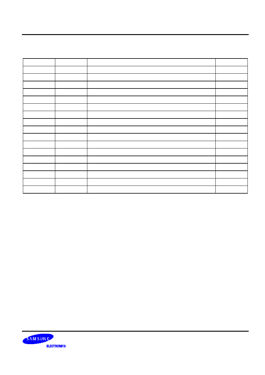
I/O CHART
Index
AINT Input (V)
Digital Output
0
0.00000 ~ 0.00293
0000000000
1LSB=2.93mV
VREF=3.2V
1
0.00293 ~ 0.00586
0000000001
2
0.00586 ~ 0.00879
0000000010
~
~
~
511
1.49707 ~ 1.50000
0111111111
512
1.50000 ~ 1.50293
1000000000
513
1.50293 ~ 1.50586
1000000001
~
~
~
1021
2.99121 ~ 2.99414
1111111101
1022
2.99414 ~ 2.99707
1111111110
1023
2.99707 ~ 3.00000
1111111111
BW1218L
0.35
µ
µ
µ
µ
m 10-BIT 510MSPS ADC
8
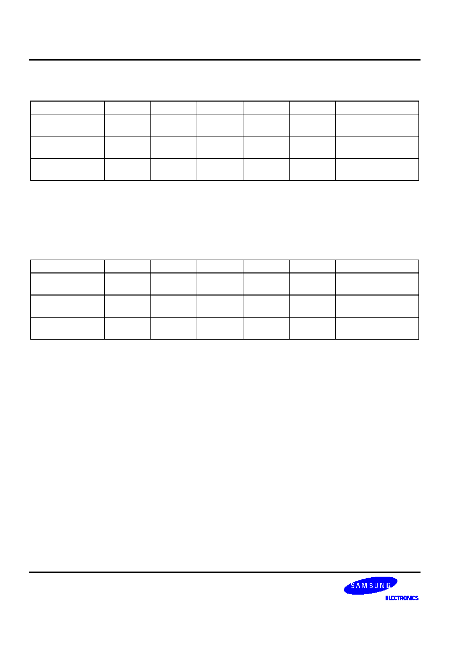
TIMING DIAGRAM
1. Main Waveform
STCB
CKIN
AINT
A2
A1
A5
Input Sampling Period
A6
A7
D1
D2
D4
D5
D3
D7
D6
EOC
DO[9:0]
2. STCB & CKIN Condition
STCB
CKIN
T
SAFE
3ns
10ns
The A/D Converter operates data conversion when STCB(Start Conversion Bar) signal is just "HIGH". Otherwise,
output data (DO[9:0]) keep the current states. The STCB signal should be changed during "T
SAFE
" with the "HIGH"
level of the clock to operation as shown in the main waveform.
3. Pipeline Delay
STCB
EOC
Pipeline Delay
After STCB is "HIGH", the A/D Converter requires the pipeline delay of 3 clock period to generate EOC signal and
data outputs.
0.35
µ
µ
µ
µ
m 10-BIT 510MSPS ADC
BW1218L
9
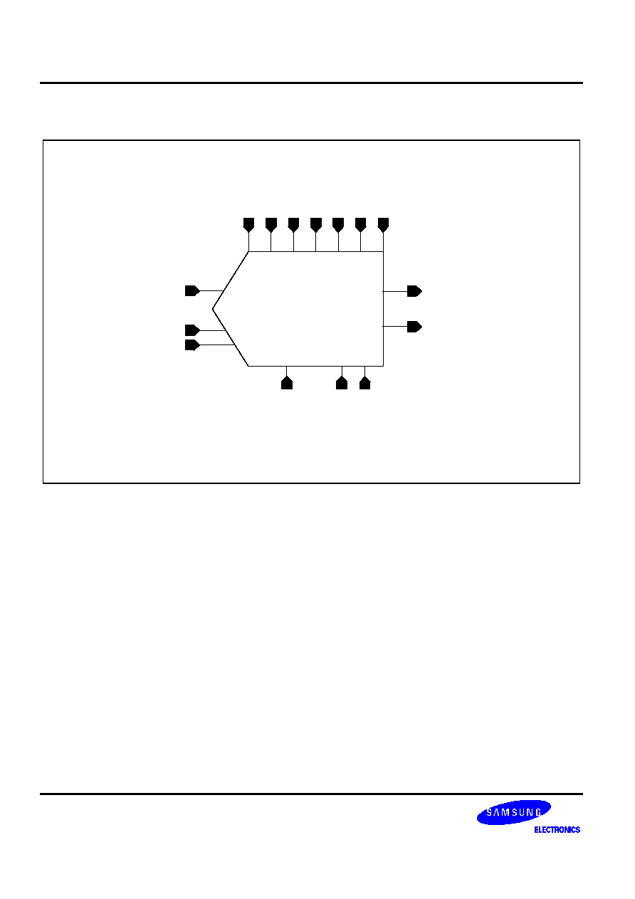
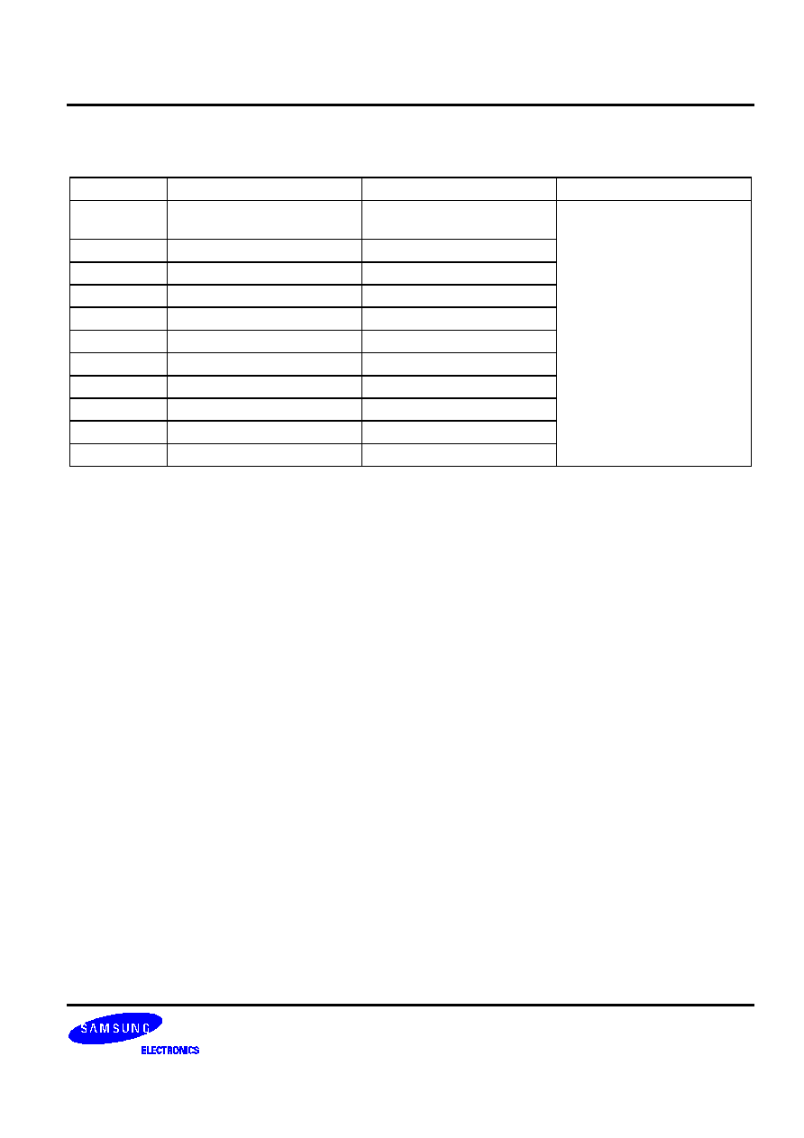
CORE EVALUATION GUIDE
1. ADC function is evaluated by external check on the bidirectional pads connected to input nodes of HOST DSP
back-end circuit.
2. The reference voltages may be biased internally through resistor divider.
BW1218L
AGND
VREF
AINT
CKI
N
SPE
EDUP
STB
Y
DO[9:0]
Digital Mux
HOST
DSP
CORE
Bidrectional
PAD
(ADC Function Test &
Externally Forced Digital Input)
DO[9:0]
DO[9:0]
DO[9:0]
EOC
VDD
A
VSS
A
VBB
A
VDD
D
VSS
D
VBB
D
STC
B
BW1218L
0.35
µ
µ
µ
µ
m 10-BIT 510MSPS ADC
10
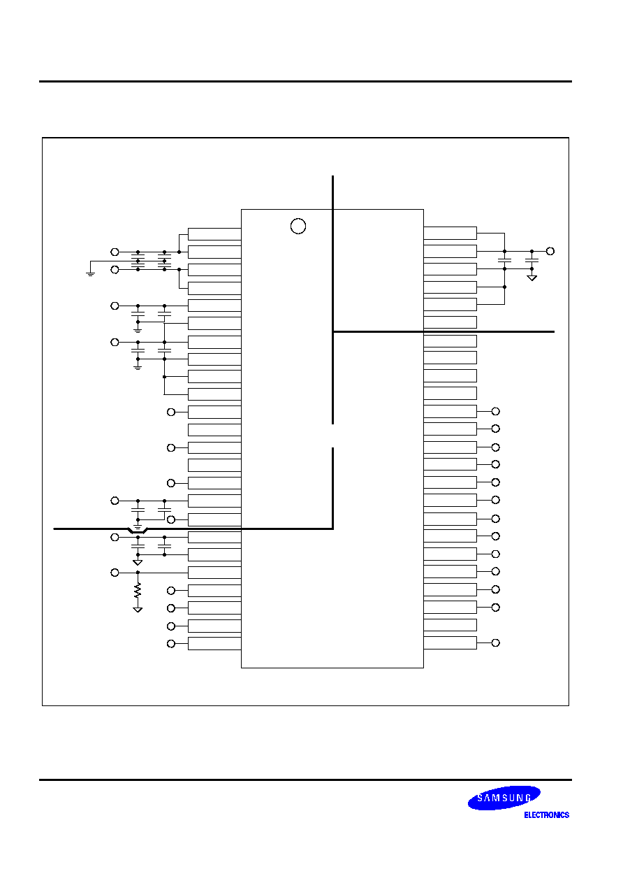
PACKAGE CONFIGURATION
48
47
NC
VREF
AGND
NC
CML
VDDA
VDDA
VBBA
VSSA
VSSA
AINT
NC
NC
NC
SPEEDUP
ITEST
STBY
VDDR
VSSR
CKIN
TEST1
TSET2
NC
NC
VDDD
VDDD
VSSD
VSSD
VBBD
EOC
NC
NC
NC
DO[9]
DO[8]
DO[7]
DO[6]
DO[5]
DO[4]
DO[3]
DO[2]
DO[1]
DO[0]
NC
STCB
46
45
44
43
42
41
40
39
38
37
36
35
34
33
32
31
30
29
28
27
26
25
1
2
3
4
5
6
7
8
9
10
11
12
13
14
15
16
17
18
19
20
21
22
23
24
0.1u
0.1u
TRIST
NC
NC
10u
50
10u
0.1u
10u
0.1u
10u
0.1u
10u
0.1u
10u
BW1218L
Digital I
Analog
Digital II
0.1u
10u
NOTE: NC denotes "No Connection".
0.35
µ
µ
µ
µ
m 10-BIT 510MSPS ADC
BW1218L
11
PACKAGE PIN DESCRIPTION
Number
Name
I/O Type
Pin Description
2
VREF
AI
Reference Voltage (3.2V)
3
AGND
AI
Analog Ground for Reference
5
CML
AB
Internal Bias Point
6, 7
VDDA
AP
Analog Power (3.3V)
8
VBBA
AG
Analog Sub Bias
9, 10
VSSA
AG
Analog Ground
11
AINT
AI
Analog Input (0.0V~3.0V)
15
SPEEDUP
DI
VDD=Speed up, GND=Normal
16
ITEST
AB
open=use internal bias circuit
17
STBY
DI
VDD=Power saving (Standby),
GND=Normal
18
VDDR
PP
PAD Power (3.3V)
19
VSSR
PG
PAD Ground
20
CKIN
DI
Sampling Clock Input
21
TEST1
AO
Monitoring (TEST) Cell Pin1,
GND=Normal
22
TEST2
AO
Monitoring (TEST) Cell Pin2,
GND=Normal
25
TRIST
DI
Tristate Buffer Input
VDD=High Impedance,
GND=Normal
27
DO[0]
DO
Digital Output (LSB)
28~5
DO[1:8]
DO
Digital Output
36
DO[9]
DO
Digital Output (MSB)
42
EOC
DO
End of Conversion Signal
43
STCB
DI
Start of Conversion Signal
44
VBBD
DG
Digital Sub Bias
45, 46
VSSD
DG
Digital GND
47, 48
VDDD
DP
Digital Power (3.3V)
NOTE: I/O
TYPE
PP
and
PG
denote
PAD
Power
and
PAD
Ground
respectively.
BW1218L
0.35
µ
µ
µ
µ
m 10-BIT 510MSPS ADC
12
PACKAGE PIN DESCRIPTION (Continued)
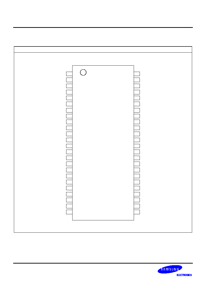
Configuration
48
47
NC
VREF
AGND
NC
CML
VDDA
VDDA
VBBA
VSSA
VSSA
AINT
NC
NC
NC
SPEEDUP
ITEST
STBY
VDDR
VSSR
CKIN
TEST1
TSET2
NC
NC
VDDD
VDDD
VSSD
VSSD
VBBD
EOC
NC
NC
NC
DO[9]
DO[8]
DO[7]
DO[6]
DO[5]
DO[4]
DO[3]
DO[2]
DO[1]
DO[0]
NC
STCB
46
45
44
43
42
41
40
39
38
37
36
35
34
33
32
31
30
29
28
27
26
25
1
2
3
4
5
6
7
8
9
10
11
12
13
14
15
16
17
18
19
20
21
22
23
24
TRIST
NC
NC
BW1218L

0.35
µ
µ
µ
µ
m 10-BIT 510MSPS ADC
BW1218L
13
USER GUIDE
1. Input Range
-- The BW1218L use only the single-ended input, and input range is 0.0V
~
3.0V (3.0V
P-P
).
2. Speed Up
The initial target speed of BW1009L is 5
~
10MHz.
If you want more speed (about
10MHz), you should connect the SPEEDUP port to 'HIGH'.
3. Power Consumption Optimization
Yon can optimize the power consumption, as control the ITEST voltage level precisely .
BW1218L
0.35
µ
µ
µ
µ
m 10-BIT 510MSPS ADC
14
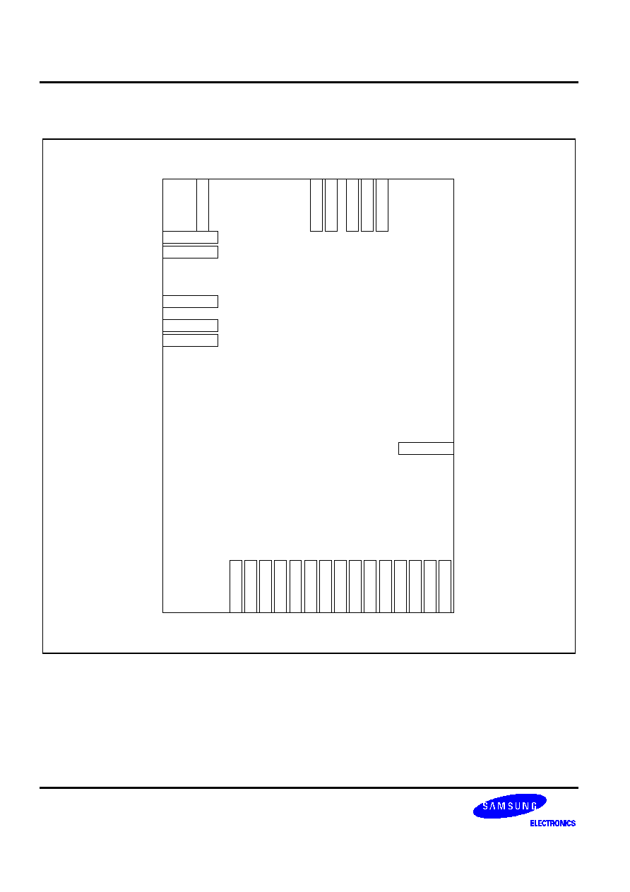
PHANTOM CELL INFORMATION
BW1218L
VDD
A
AGN
D
VRE
F
VDD
D
VSS
D
VBB
D
VBBA
VSSA
AINT
SPEEDUP
STBY
STCB
DOU
T
[0
]
DOU
T
[1
]
DOU
T
[2
]
DOU
T
[3
]
DOU
T
[4
]
DOU
T
[5
]
DOU
T
[6
]
DOU
T
[7
]
DOU
T
[8
]
DOU
T
[9
]
EOC
CKI
N
VBB
D
VSS
D
VDD
D
0.35
µ
µ
µ
µ
m 10-BIT 510MSPS ADC
BW1218L
15
PHANTOM CELL INFORMATION (Continued)
Pin Name
Pin Usage
Pin Layout Guide
VDDA
External
- Do not merge the analog powers with another power
VSSA
External
from other blocks.
VBBA
External
- Use good power and ground source on board.
VDDD
External
VSSD
External
VBBD
External
AINT
External/Internal
- Do not overlap with digital lines.
- Maintain the shortest path to pads.
VREF, AGND
External/Internal
- Maintain the larger width and the shorter length as far as the pads.
- Separate from all other digital lines.
SPEEDUP
External/Internal
- Separate from all other analog signals
CKIN
External/Internal
STBY
External/Internal
STCB
External/Internal
EOC
External/Internal
- Separated from the analog clean signals if possible.
ADO[9]
External/Internal
ADO[8]
External/Internal
ADO[7]
External/Internal
ADO[6]
External/Internal
ADO[5]
External/Internal
ADO[4]
External/Internal
ADO[3]
External/Internal
ADO[2]
External/Internal
ADO[1]
External/Internal
ADO[0]
External/Internal
BW1218L
0.35
µ
µ
µ
µ
m 10-BIT 510MSPS ADC
16
FEEDBACK
REQUEST
ADC Specification
Parameter
Min
Typ
Max
Unit
Remarks
Supply voltage
V
Reference Input voltage
V
Analog Input voltage
Vpp
Operating temperature
°C
Integral non-linearity error
LSB
Differential non-linearity error
LSB
Offset voltage error (Bottom)
mV
Offset voltage error (Top)
mV
Maximum conversion rate
MSPS
Dynamic supply current
mA
Power dissipation
mW
Signal-to-noise ratio
dB
Digital output format (Provide detailed
description & timing diagram)
·
What do you want to choose as power supply voltages? For example, the analog VDD needs to be 5V. the
digital VDD can be 3.3V/5V.
·
What resolution do you need for ADC?
·
How about conversion speed (data in ® data out)?
·
How many cycles do exist during the latency of ADC (pipelined delay)?
·
What's the input range? And then what do you need between single input and differential input?
·
Can the bus interface be compatible with TTL?
·
Could you explain external/internal pin configurations as required?
Specially requested function list :
0.35
µ
µ
µ
µ
m 10-BIT 510MSPS ADC
BW1218L
17
HISTORY CARD
Version
Date
Modified Items
Comments
ver 1.0
Original version published (preliminary)
ver 1.1
ver 1.2
ver 1.3
ver 1.4
ver 1.5
2000.11
Release the formal datasheet
ver 1.6
02.04.29
Add the pin information to the phantom cell information

BW1218L
0.35
µ
µ
µ
µ
m 10-BIT 510MSPS ADC
18
NOTES